
Abstract
Abstract
Fabrication of composite microstructures comprising more than one type of material has been a fundamental challenge in nanotechnology. In this study, we report a method that can be used for the direct fabrication of complex three-dimensional (3D) polymer/metal hybrid microstructures. The patterning of materials (a polymer and a metal coatable polymer) in selected regions was achieved by a two-photon stereolithography process using a dual-stage scanning process. A precise alignment process was perfected to achieve the coincidence of polymeric and metal-coated polymer components of the microstructure. Selective metallization of the metal coatable polymer microstructure was performed through silver deposition by means of electroless plating. The 3D microcoil was demonstrated and electrically characterized.
Introduction
A three-dimensional (3D) coiled shape is crucial for microcoils to achieve a reasonable quality factor (Q). However, the fabrication of functional 3D microcoils has remained difficult with conventional patterning techniques.1–6 For these reasons, the development of alternative direct 3D patterning techniques to fabricate 3D microcoils, which are useful for compact wireless communication devices, wireless power transmission, and small antennas, has attracted much attention.
In previous studies in the literature, 3D microcoils could be fabricated using automatic wire bonders 7 and inkjet printing. 8 However, the fabrication resolution and feasible shapes were limited. One of the most promising alternative techniques to build 3D microstructures is the direct patterning process, which is based on two-photon polymerization (TPP).9–12 A two-photon stereolithography (TPS) process using TPP is an effective method to fabricate 3D polymer microstructures. However, additional functionality, such as electrical conductivity, must be achieved to enable these microstructures to be used in functional nano/microdevices.
Electrical conductivity is a fundamental requirement for transferring signals and powering microsystems. The fabricated polymer structure can be transformed into an electrically conductive metal structure through an electroless plating process that provides uniform coating of various metals (Ag, Cu).13–16 This allows fabrication of 3D conductive microstructures onto glass substrates. High functional devices such as electrical components are composed of hybrid materials, including metal patterns for electrical conductivity and polymer patterns for insulation. Therefore, a hybrid material (polymer/metal) patterning technology is needed to fabricate a realizable 3D electrical device that is composed of polymer and metal materials.
In this study, we report an effective approach for directly fabricating 3D microcoils with desirable electrical functions. Patterning a hybrid material (a polymer and a metal coatable polymer) in selected regions is achieved by a two-photon stereolithography process using a dual-stage scanning process (TPS-D). For precise alignment of the polymer and metal coatable polymer structures to form hybrid material microstructures, a pattern-to-pattern comparison method is used for the first time. Selective metallization of the metal coatable polymer structure is performed through silver deposition by electroless plating.13–19,26 This approach enables the fabrication of a selective metal-coated 3D polymer/metal microstructure with ultrahigh precision for use in various nano/microscale devices with electronic, optoelectronic, or electromechanical functions.
Fabrication System for 3D Microstructure
A schematic diagram of the experimental setup is presented in Figure 1. TPS-D consists of linear motor stages and piezoelectric stages. For the two-photon absorption phenomena, a femtosecond laser (mode-locked Ti-sapphire laser) was used as a laser beam source; this laser had a wavelength of 780 nm, ultrashort pulse duration of less than 100 fs, and repetition rate of 80 MHz. A λ/2 plate and a polarizing beam splitter were used to control the laser power. An optical shutter, which has a maximum frequency of 1.0 kHz, was used for expeditious control of the on/off state of the laser beam. The femtosecond laser beam was tightly focused using an oil immersion objective lens (100 × magnifications, numerical aperture of 1.3). During laser beam scanning, the laser beam was fixed and tightly focused at a given position and the specimen was moved three dimensionally with piezoelectric stages. The polymer resin prepared on the substrate was fixed on a dual stage using a jig. The specimen was positioned at the starting point of the laser beam path using motor stages with 300 nm resolution. Then, arbitrary 3D polymer structures were fabricated using the computer-controlled three-axis piezoelectric stages with 0.1 nm resolution. A high-magnification charge-coupled device (CCD) camera was used for the adjustment of the focused laser beam and for real-time process monitoring.
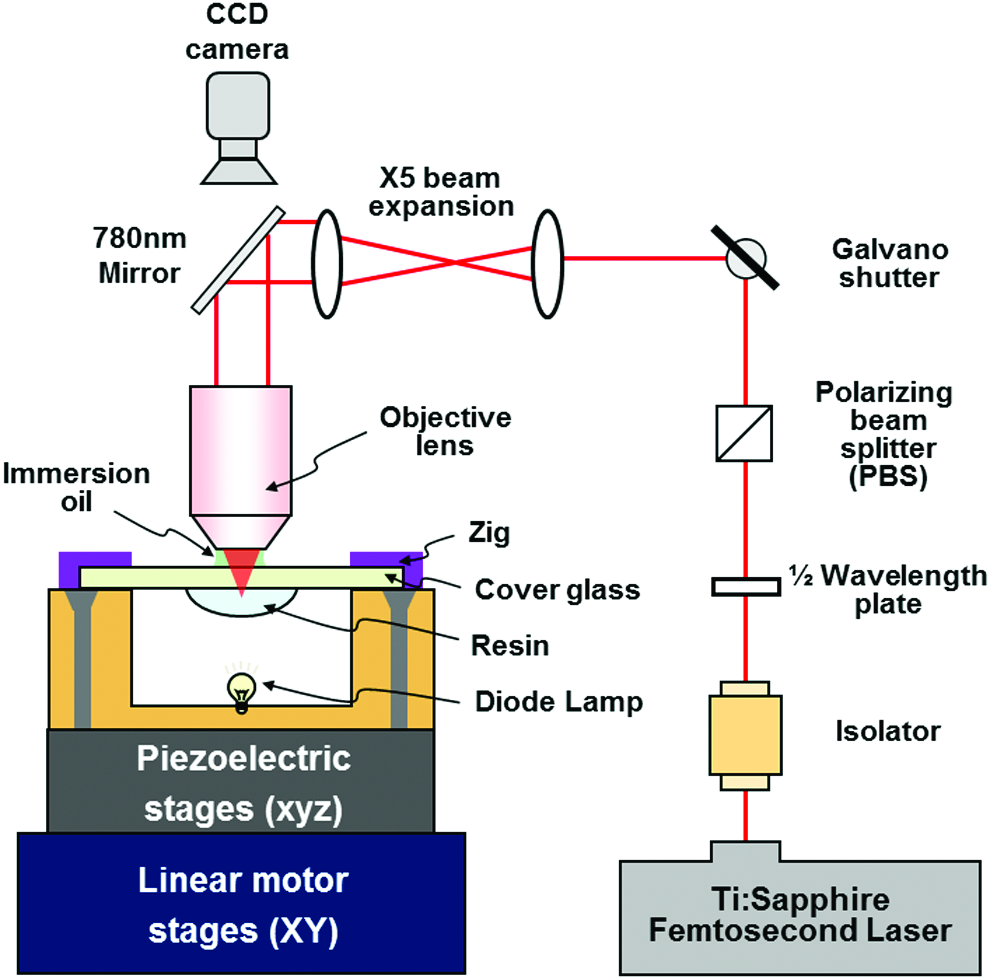
Schematic diagram of the developed two-photon stereolithography system using dual-stage scanning. Color images are available online.
Results
Design of 3D microcoil
The proposed TPS-D can be used for the facile fabrication of polymer/metal hybrid microstructures that are composed of polymer structure and metal-coated polymeric structure. Such 3D electrical structures are difficult to fabricate with conventional processes. The resonance frequency of the 3D microcoil allows having flexibility according to the design of 3D microcoil. In this article, we designed the 3D microcoil with a diameter of 200 μm, a height of 60 μm, and 5 turns.
The inductance and self-capacitance of a coil can be calculated from its dimensions, forming the number of turns according to the parallel equivalent circuit model using equations [Eqs. (1–3)].20,21
Here L is the inductance (nH), N is the number of turns, D is the loop diameter (mm), H is the height (mm), C is the self-capacitance (pF), ɛr is the dielectric constant, s is the turn spacing (mm), d is the coil diameter (mm), and f0 is the resonance frequency (Hz). Using these equations, the theoretical inductance and self-capacitance values for the coil can be calculated. The ideal inductance and self-capacitance are about 6.67 nH and 0.0062 pF, respectively, and the expected electromagnetic resonance frequency is 24.79 GHz. This result shows that the proposed 3D microcoil can be used for high-performance electrical components such as a wireless power transmission device.
3D-printed microcoil
We previously reported various techniques for the realization of complex 3D polymer microstructures using the TPS process.11,22–25 In addition, we developed a dual-stage femtosecond laser scanning process for fabricating aligned hybrid microstructures that constitute both polymer and metal-coated polymer microstructures. A schematic diagram of the experimental setup is presented in Figure 1. The 3D microcoil was fabricated by TPS-D and selective electroless plating processes.
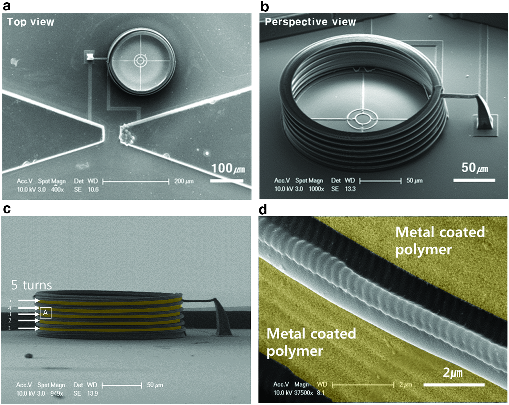
A silver-coated coiled structure was fabricated in three distinct steps. At first a cylindrical structure was fabricated with SU-8 (MicroChem Co.) and its surface was modified to make it suitable for silver coating. The second step involved creating coiled spacer patterns on the cylindrical structure fabricated from urethane/acrylate photoresists (SCR 500). In the final step, silver was selectively coated on the SU8 part of the microstructure by immersing the whole structure in a silver bath. These processes are described in detail below. As shown in Figure 2a, micropatterns that act as electrical pads for the connection with external measuring equipment were patterned by conventional UV photolithography with SU-8 resin. A drop of SU-8 resin sensitized with a two-photon chromophore was placed on a cover glass substrate, as shown in Figure 2b. A drop of SU-8 was prebaked at 95°C for 15 min. With the developed TPS-D with a laser power of 300 mW and laser scanning speed of 100 μm/s, the SU-8 microstructure aligned with the prefabricated patterns on the substrate was fabricated, as shown in Figure 2c. This structure acted as a support for the spiral coil structure and the metal-coated part. After the laser scanning process, the sample was postbaked at 95°C for 15 min. The remaining resin was washed away with propylene glycol methyl ether acetate (PGMEA) as a solvent, as shown in Figure 2d. The surfaces of the polymer microstructures were functionalized with amine groups by treating them with 1,3-diaminopropane [NH2(CH2)3NH2] in the presence of butyl lithium for 5 min, after which they were rinsed thoroughly in ethanol, as shown in Figure 2e. 26 The amine groups undergo a Michael addition reaction with unreacted surface epoxides. This reaction creates surface-bound amine-terminated amides. 27 Amines are capable of reducing gold ions from solutions of gold salts. Gold nanoparticles were generated on the surfaces of the SU-8 structures by immersing in aqueous AuCl4− (5.3 × 10⁻⁴ M aqueous HAuCl4 for 1 h) and reducing with NaBH4 (0.1 M aqueous NaBH4 for 5 min). These gold nanoparticles are capable of acting as seeds that can initiate further metal deposition on the polymeric surfaces under favorable conditions. For fabrication of the second structure, which was a spiral insulating coil, modified SCR-500 (Japan Rubber Co.) resin was used, as shown in Figure 2f. Unlike structures fabricated with SU-8 resin, the structures fabricated from SCR-500 resin can be clearly distinguished from the unpolymerized resin owing to the refractive index change in the polymerized structures. This enables the real-time monitoring of the fabrication process with a CCD camera. The real-time monitoring capability facilitates the alignment of different structures (surface-functionalized polymer structures for metal-coated structures and polymer structures for insulation) with other structures. As shown in Figure 2g, the center of the spiral coil structure must be aligned exactly with the center of the prefabricated supporting structure. Generally, the use of a view-finder in a CCD camera system with an index line is sufficient to align the patterns with each other. However, the focused image varies depending on the condition, such as the amount, position, and different optical properties of the dropped resin in this system. Therefore, for a precise alignment of structures, a pattern-to-pattern comparison method was used to realize the possibility of direct patterning during the TPS-D process.

Schematic diagram of the fabrication process flow.
Figure 3 shows the pattern-to-pattern comparison method used in this process. Several primary mark patterns were fabricated, as shown in Figure 3a and b. After developing the remaining primary resins (SU-8), another polymer resin (SCR-500) was dropped. Then, it was possible to fabricate the secondary mark pattern in the center of the prefabricated primary mark pattern using a CCD vision system, as shown in Figure 3d. The errors of the x and y axes compared with the primary mark pattern and the secondary mark pattern can be measured using the CCD vision system and piezoelectric stages as shown in Figure 3c. Using this method, the x and y axes on the stages can be aligned to the original positions, and the aligned primary and secondary mark patterns can be fabricated, as shown in Figure 3e and f. With this pattern-to-pattern comparison method, the insulating coil structure with the modified SCR-500 resin could be fabricated in alignment with the prefabricated supporting structure made by SU-8 resin. After the residual SCR-500 resin is washed away with ethanol, the polymer spiral structure acts as insulation for the 3D metallic microcoil, as shown in Figure 2h. Finally, silver nanoparticles are selectively deposited onto the functionalized surface of the polymer structure using an electroless coating process, as shown in Figure 2i. The electroless silver coating solution was prepared by mixing 12 mL of 33 wt% aqueous gum Arabic, 1 mL of 1.5 M citric acid, 1 mL of 0.5 M trisodium citrate, 3 mL of 37 mM aqueous silver lactate, and 3 mL of 0.52 M aqueous hydroquinone. 18 The silver coating time was 60 min to achieve a thickness of 100 nm. The silver-coated samples were rinsed with deionized water and isopropanol. The cleaned silver-coated sample was annealed at 200°C for 30 min. The measured electrical resistivity was 2.0 × 10⁻⁵ Ω·cm. Although this resistivity is nearly 12.5 times higher than that of bulk silver (1.59 × 10⁻⁶ Ω·cm), this result signifies that electroless silver-coated structures are good electrical conductors that can be readily used in electronic devices. The discrepancy between the resistivity of the silver-coated pattern and the bulk resistivity value could be mainly due to the electron scattering caused by the surface roughness (Rrms ∼ 10 nm) and irregular aggregated silver nanoparticles. Figure 4 shows a fabricated 3D microcoil with a diameter of 200 μm, a height of 60 μm, and 5 turns. Silver coating occurs selectively on the SU-8 surface functionalized with gold nanoparticles, as shown in Figure 4d. The total fabrication time for the 3D microcoil is about 5 h, including TPS-D and selective metal coating process.
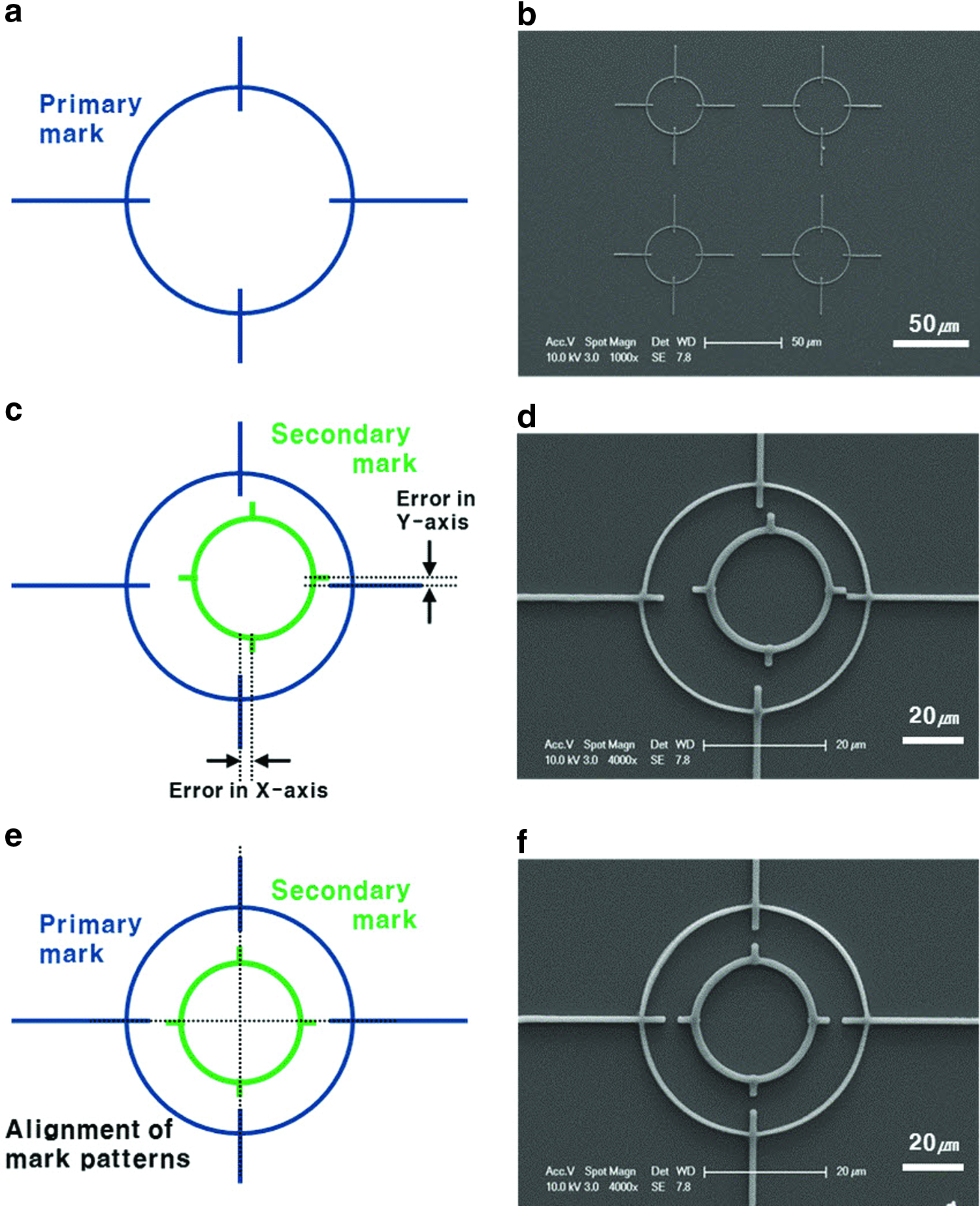
Pattern-to-pattern comparison method.
To compare the measured resonance frequency with theoretical calculations (24.79 GHz), the frequency characteristics of the fabricated 3D microcoil were measured using a network analyzer (Agilent, E8364B). Figure 5 shows the measured |S11| value of the fabricated 3D coil. A resonance frequency was detected at 25.4 GHz. The measured return loss drops to almost −30.03 dB at the resonance frequency. These results show that the measured resonance frequency (25.4 GHz) is a reasonable value when considering errors, such as skin effect and the metal-coated surface roughness (Rrms ∼ 10 nm). This result shows that the demonstrated 3D coil can be operated as a small antenna that can be readily used for high-performance electrical components such as low-power transfer applications. The new concept of microdevices for electronic, optoelectronic, or electromechanical applications can be studied using the wirelessly transferred electrical signal.
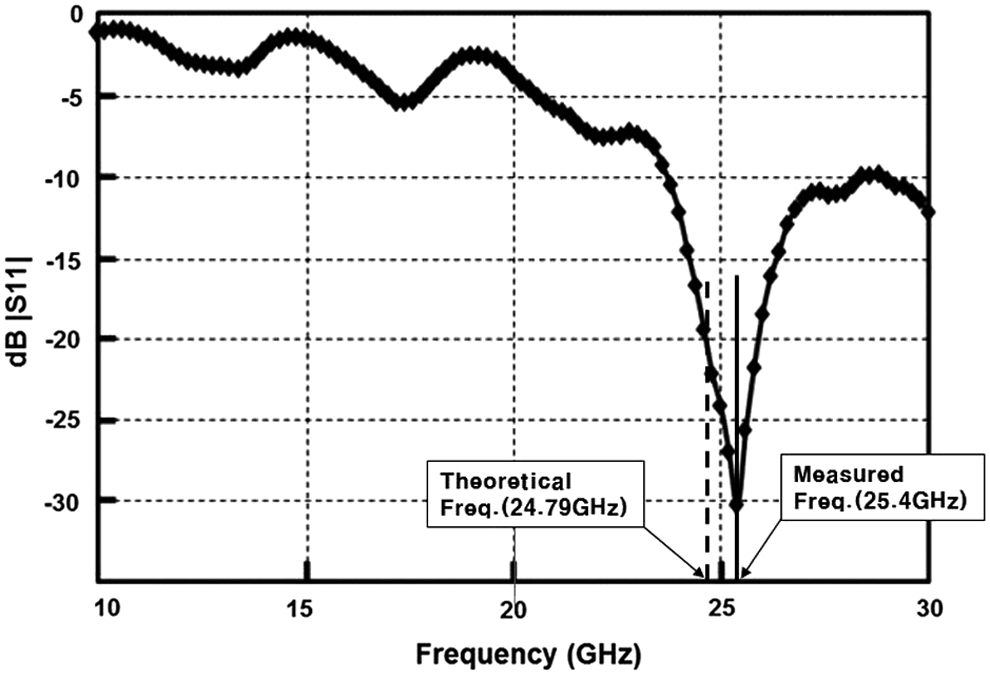
This graph shows the measured |S11| values of the 3D microcoil as a function of frequency.
Conclusions
In summary, we have demonstrated a direct 3D fabrication method for integrating precisely aligned polymer/metal hybrid microstructures composed of conductive metal-coated polymer and nonconductive polymer structures by TPS-D and selective electroless plating. For precise alignment of the hybrid material structures, a pattern-to-pattern comparison method was used. The fabricated 3D microcoil is operated at 25.4 GHz, which is useful for compact wireless communication devices, wireless power transmission, and small antennas. Therefore, the suggested technique offers remarkable advantages as a direct, high-resolution, 3D metal-patterning process that is applicable to precise nano/microscale devices with electronic, optoelectronic, or electromechanical functions.
Footnotes
Acknowledgment
This work was supported by the KITECH internal project and basic science research program (2017R1C1B5077130) of the National Research Foundation of Korea.
Author Disclosure Statement
No competing financial interests exist.