
Abstract
As an emerging additive manufacturing technology, inkjet printing has been increasingly applied in microelectronics field. However, due to the impacting and rebounding behaviors of conductive ink droplets impinging onto flat substrates, it is challenging to fabricate conductive lines with desired quality, such as suitable line width and line thickness, and matching resistance when it is used for interconnecting multifarious electronic components if there is not a proper configuration of operating parameters. To address this research gap, this article aims to investigate the effect of process parameters on the quality of conductive lines, including the platform temperature, printing speed, number of layers, and delay time (droplet interarrival time), are selected to conduct a full factorial experiment. First, the approximate parameter ranges for ensuring the continuity of conductive lines are determined. Second, this study analyzes the interactive effect among process parameters on line quality. Third, an artificial neural network (ANN) is constructed to predict the quality of printed lines. Results show that the line width does not increase with an increased number of layers, while the line thickness shows an increasing trend. The low resistance and high aspect ratio of printed line are achieved by printing 5 layers with the platform temperature of 70°C, the delay time of 12.2 ms, and the printing speed of 1139.39 mm/min. Moreover, the ANN model can be used to predict line width and line thickness with excellent performance, except for the resistance due to the irregular line edge. This study provides a useful guide for the selection of appropriate printing parameters to realize a diverse range of quality properties for 3D printed conductive lines in integrated circuits.
Introduction
Electronic elements are small modular components, which are interconnected together by conductive lines to control the flow of current with the aim to process information. 1 The miniaturized method for manufacturing integrated circuits will be inevitably employed due to the increasing complexity of electronic product design and applications. Traditionally, the printed electronic board is manufactured with selective corrosion on dielectric substrate by photoetching technique, followed by electroplating conducive lines on the substrate. 2 This process is relatively expensive and time-consuming due to the needed machining equipment and multistage chemical postprocessing. 3 Alternatively, inkjet printing (IJP) has attracted extensive attention in the manufacturing of semiconductor, 4 electrochemical sensors, 5 stretchable thin-film electrodes, 6 and wearable electronic devices. 7 As one of the microscale additive manufacturing (MAM) techniques, IJP is a liquid-phase deposited technique. It also provides a promising approach to free the conductive pattern design whether on rigid or flexible substrates. This possesses great potentials in integrated electronic industries.
To satisfy the requirement of high density in integrated circuit, the line width needs to be of <1 mm with low resistance. At the same time, the printed lines should be controlled at a suitable thickness, neither too thick nor too thin without causing packaging or interconnected problems. Additionally, the precise deposition of inkjet droplets on substrate and the formation of conductive lines with smooth layer are big challenges to get uniform thickness of printed lines. Therefore, the width, resistance, and thickness of conductive lines need to be properly controlled to satisfy quality requirements of the integrated circuit.
It is well known that the factors affecting line width, resistance, and line thickness include: curing method, ink properties, and jetting parameters. Plasma pretreatment, 8 infrared radiation sintering, 9 laser annealing, 10 and electrical sintering 11 have been widely used as curing methods.12,13 Unfortunately, the long-time exposure to high temperature can generate microcracking due to substrate shrinkage. Moreover, the large pores and porosities are hard to eliminate using sintering treatment. 14 To address this problem, much research has been done on the preparation of conductive ink to improve the printed quality. The silver-based ink, 15 biocompatible conductive ink, 16 gold ink, 17 and graphene ink 18 have proved their feasibility in enhancing conductivity and the adhesive force between conductive lines and dielectric substrates. The comparatively high cost and time consumption are inevitable. Another way of improving the line quality is to optimize process parameters. The effects of drop spacing, contact angle, substrate temperature, and substrate types on the 3D shape of straight lines (cross section area, width, height, or thickness) were investigated.19,20
However, the conductivity of printed lines was not considered in analyzing the formation process of geometric morphology. The basis of optimizing process parameters was guaranteeing the desired line shape (parallel-sided line without bugling and breakpoint 21 ) on the premise of ensuring normal conductivity and establishing the corresponding parametric models used for predicting line quality with the aim to reduce unnecessary workloads. Since the electrical and dimensional properties of printed lines were directly related to the performance of the printed electronics, it was significant to understand their characteristics in manufacturing the highly reliable products. Hitherto, the fabrication of desired conductive line still heavily relies on seasoned practitioners for IJP of a kind of certain conductive ink. The fundamental relationship between process parameters and line quality (such as line continuity, line width, resistance, and line thickness) was not fully understood due to the highly coupling effects between the process parameters and ink properties.
Therefore, the aim of this research is to investigate the formation mechanism of conductive lines during IJP of a nano-silver ink under various process parameters and evaluate the single and interactive effects of the operating parameters on the formed-line performance through combining the experimental observations and the estimation of predicted models using relative error. The proposed process parameters were platform temperature, printing speed, number of layers, and delay time (droplet interarrival time). First, the effective range of process parameters to obtain continuous conductive lines were determined through controlling variable method. Then, the full factorial experimental scheme L625 (54) was designed and experiments were performed. The main effect analysis and joint analysis were normally employed, followed by making an evaluation for the built prediction models. Finally, the multiobjective optimization method was adopted to obtain the optimal parameter configurations and verification was also conducted through an additional experiment.
The main motivations for grasping the effects of the process parameters on line continuity is to improve the knowledge regarding how to obtain printed lines with desirable size but not sacrifice high conductivity. The obtained results in this study can be used to provide the process designers a valuable and pivotal reference (with the purpose of clearly understanding the process of microstructure formation from silver-nanoparticle inks as well as predict the nanoparticles' self-assembly conductive lines based on targeted responses) to configurate parameters in fabricating conductive lines of well-defined shape without bulging and gullying applied in diverse integrated electronics.
Literature review
IJP is one of the most reliable additive manufacturing (AM) processes for electronic circuit fabrication with high degree of freedom, high density, and desired customization. For the IJP technology, the width of fabricated conductive lines mainly depended on the original droplet size and its expanded range on the substrate. 22 Although the droplet size can be diminished through decreasing the nozzle diameter, this produces a constraint for surface tension and viscosity of the inks and thereby restricts the selection of conductive inks. 23 Furthermore, the satellite droplets and the ligament of droplets can be emerged during the falling process.24,25 This phenomenon will cause the size deviation or scatter in random locations after impacting substrate due to aerodynamic and gravitational forces. As a result, the unsmooth external morphology of printed lines will exist. Hence, the effect of the voltage on the generation of droplets was fundamentally discussed through shifting different driving waveforms (bipolar, unipolar, and arbitrary shape).26,27 It was found that the adjustment of the dwell voltage and dwell time was pivotal to gain ideal droplets in terms of the volume and shape.
Nevertheless, only considering voltage is unwise for the generation of ideal droplets and it will trigger the matter of discontinuous and bulging lines after depositing multilayer drops. Mu et al fabricated uniform lines by varying droplet spacing. 28 Ning et al printed droplet array with optimized drop spacing to obtain 100 μm line width. 29 Whereas, controlling the drop spacing is arduous and unproductive for fabricating the conductive lines due to the complexity of internal flowing and overlap-evolved mechanism.
Subsequently, Hamad et al explored the process parameters (waveform dwell voltage, printing speed, and drop spacing) on the quality of conductive lines using single-factor analysis, which indicated that better uniform lines can be printed with optimized process parameters on the poly-ether-ether-ketone substrate. 30 Moreover, Wang et al explored the effect of the number of layers, the heat treatment temperature, the drop frequency, and the number of the nozzles on photoelectric properties of nano-silver lines. 31 It was suggested that the accumulation and overflow of silver ink at the edges resulted in a decrease in printing accuracy. Xing et al adjusted cross-sectional geometries of the conductive lines easily by regulating parameters such as the printing speed, applied pressure, micronozzle/substrate distance, and number of stacks. 32 The interactive effect of process parameters on conductive lines is not considered. It is still insufficient to investigate the global range of process parameters for guaranteeing the continuity of silver-ink lines from abovementioned literatures.
Inspired by the study of process parameters, Ball et al established a Taguchi regression analysis model to predict the droplet diameter. 33 It is suggested that the predicted and measured results are very close to each other. Similarly, the response surface methodology presented by Laurila was used to build a function between line width and process parameters (voltage and frequency) to predict the line width. 34 The traditionally mathematical modeling can verify the influence of process parameters on a certain performance of conductive lines; it is difficult to accurately establish the mapping relationship between input and output variables.
Although some preliminary researches have been done, research on analyzing the interactive relationship between parameters and conductive line qualities remains undiscovered. The identified range of process parameters lacks reasonable explanation when performing experimental investigation. 22 Beyond that, it cannot meet the requirement for developing a comprehensive modeling to forecast the line quality before real fabricating. To address these shortcomings, the article presents a comprehensive method integrating data analysis and quality prediction to reveal the effect of process parameters on the line width, resistance, and line thickness. It is expected that this study will provide full insight into the relationship between the line formation and process parameters, which can lay a solid foundation in parameter configuration for manufacturing the high-performance circuits and functional devices to deal with complicated and customized application scenarios.
Experimental Study
Experimental setup
The conductive ink has two types, organic ink and inorganic ink. The organic ink, which is a type of material with good flexibility and poor conductivity, mainly includes oxidized graphene, reduced graphene, carbon nanotubes, and carbon black. 35 The inorganic ink materials include copper, gold, and silver. The copper possessed desired conductivity, whereas the dense oxide film will be formed on its surface due to strong oxidation after long-term deposition in the air, which will lead to nonnegligible effect on conductivity. 36 The gold is too expensive to use. 37 The silver is a good electrical conductor, not easy to oxidize in air, and cost is much less than gold. Therefore, the nano-silver ink has become the primary choice in the field of electronic AM. In this work, the nano-silver ink with the particle size of 100 nm and the density of 2.56 kg/L manufactured by Henkel Corporation is used. The viscosity of the ink is 12,000.0 mPa·s and the silver concentration is 74.6 wt%. The bulk resistivity of the ink is <0.02 Ω when sintered at 93°C for 15 min.
The unique advantages of the nano-silver ink lie in the high viscosity and low curing temperature compared with other types of silver inks. The other physical properties of conductive ink are also displayed in Table 1. The milk-white polyethylene terephthalate (PET) sheet is chosen as the dielectric substrate with the thickness of 0.345 mm. There is no special coating on the PET substrate. The PET substrate is cleaned with ethanol before printing.
The Physical Properties of Nano-Silver Ink
RVT, the type of viscometer, which mainly used for measuring the medium viscosity of solution; VOC, volatile organic compounds.
Figure 1 shows the experimental setup of the IJP printer. The X, Y, and Z stages of the IJP machine are driven by ball screw with the motion accuracy of ±0.005 mm. The working range of the machine is 120 mm × 200 mm × 110 mm. The 5-axis motion of the machine and pulse generation for adjusting droplet ejection are controlled by computer numerical control program. The axis A and C are driven by servo motor and reducer (gear reduction ratio = 1:180) with motion accuracy of ±0.05°. The PET substrate can be heated up to 150°C. The substrate is heated to precure conductive ink to avoid the edge flow of printed lines. The piezoelectric valve controller is used to fill the reservoir with ink and ensuring that the tip of jetting device is clean. Based on the operational experience, the optimal positive pressure (245 kPa) is applied to ensure that the ink is running out of the nozzle to generate a stable droplet. This printer uses the piezoelectric drop on demand technology to eject droplets through microdrop nozzle. As shown in Table 2, the APJ1500 nozzle (100 μm opening nozzle equipped with 150 μm firing pin) manufactured by Shenzhen Axxon Piezoelectric Technology Co., LTD, is used.

Experimental setup of the inkjet printing system.
The Physical Parameters of Printhead APJ1500
As shown in Figure 2a, different combinations of process parameters were used to manufacture the conductive lines. The length of conductive line is 50 mm. The line width was measured by the electron microscope at a magnification of 400 × , as shown in Figure 2b; the resistance of conductive line was acquired by DC resistance tester (VICTOR 6310A). The deposited line thickness after drying was calculated by subtracting the thickness of pure PET sheet from the total thickness of printed lines and PET substrates, which was measured by micrometer caliper (Mitutoyo). The width and thickness in left, middle, and right positions of the printed lines were measured and the average values of the three measurements were used. Finally, all the printed lines were sintered in an oven at 60°C for 120 min according to the sintering regulation recommended by the ink supplier.
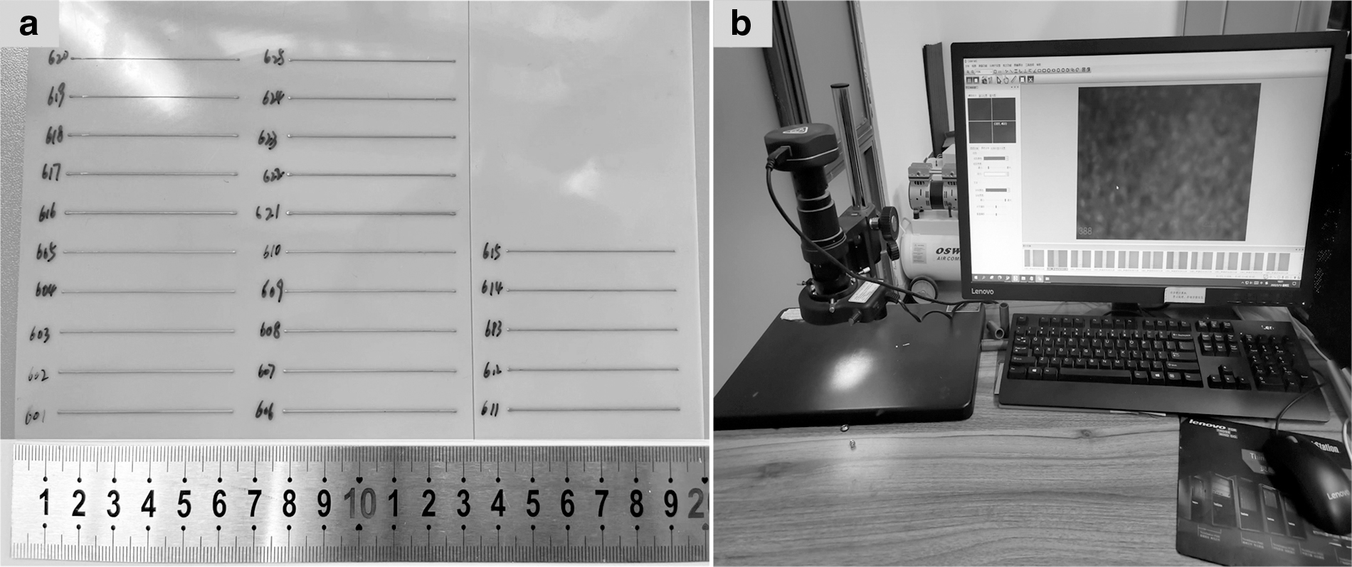
The printed samples and measured equipment:
Process parameter configurations
The continuity of a conductive line is basic requirement for microelectronics application. It can be seen in solid line border of Figure 3 that with an increase of the number of layers, the continuity of conductive line has changed distinctly while at the printing speed of 1700 mm/min, and at the nozzle ejection delay time of 14 ms. Whereas, the breaking point still exists in printed line even if printing 3 layers. As the print speed varies from 1800 to 1900 mm/min at the nozzle ejection delay time of 14 ms, the line continuity becomes worse and resembles an arrangement of breakpoints one by one, as represented in single dotted line border of Figure 3. It can be further seen in double dotted line border of Figure 3 that the two droplets can be connected, whereas the overall line is still in a disconnected state. Therefore, setting up the print speed at more than 1700 mm/min cannot guarantee the continuity of conductive lines.

The images with a magnification of 400 × for observing continuity of conductive lines at a nozzle ejection delay time of 14 ms with platform temperature of 60°C. n, number of layers; V, printing speed.
When keeping the printing speed at 1600 mm/min and changing the delay time from 14 to 16 ms, the conductive line is almost in the shape of the sugar gourd skewers as demonstrated in solid line border of Figure 4. Furthermore, this defect can be alleviated with increased number of printed layers. The bulging phenomenon of the lines is unavoidable due to increased delay time, which will deteriorate the conductivity, as shown in double dotted line border of Figure 4. The single dotted line border of Figure 4 shows that the printed line is in a continuous state and accompanied by jagged edges. The irregular line edge will lead to a dramatic increase in resistance. When the conductive line accumulates 3 layers, the morphology almost presents a stable, smooth, and continuous state. Hence, the maximum value of delay time should not exceed 14 ms when setting the printing speed as 1600 mm/min. In the meanwhile, when the relatively small delay time and the lower printed speed are selected, the droplet accumulation will occur on substrate.
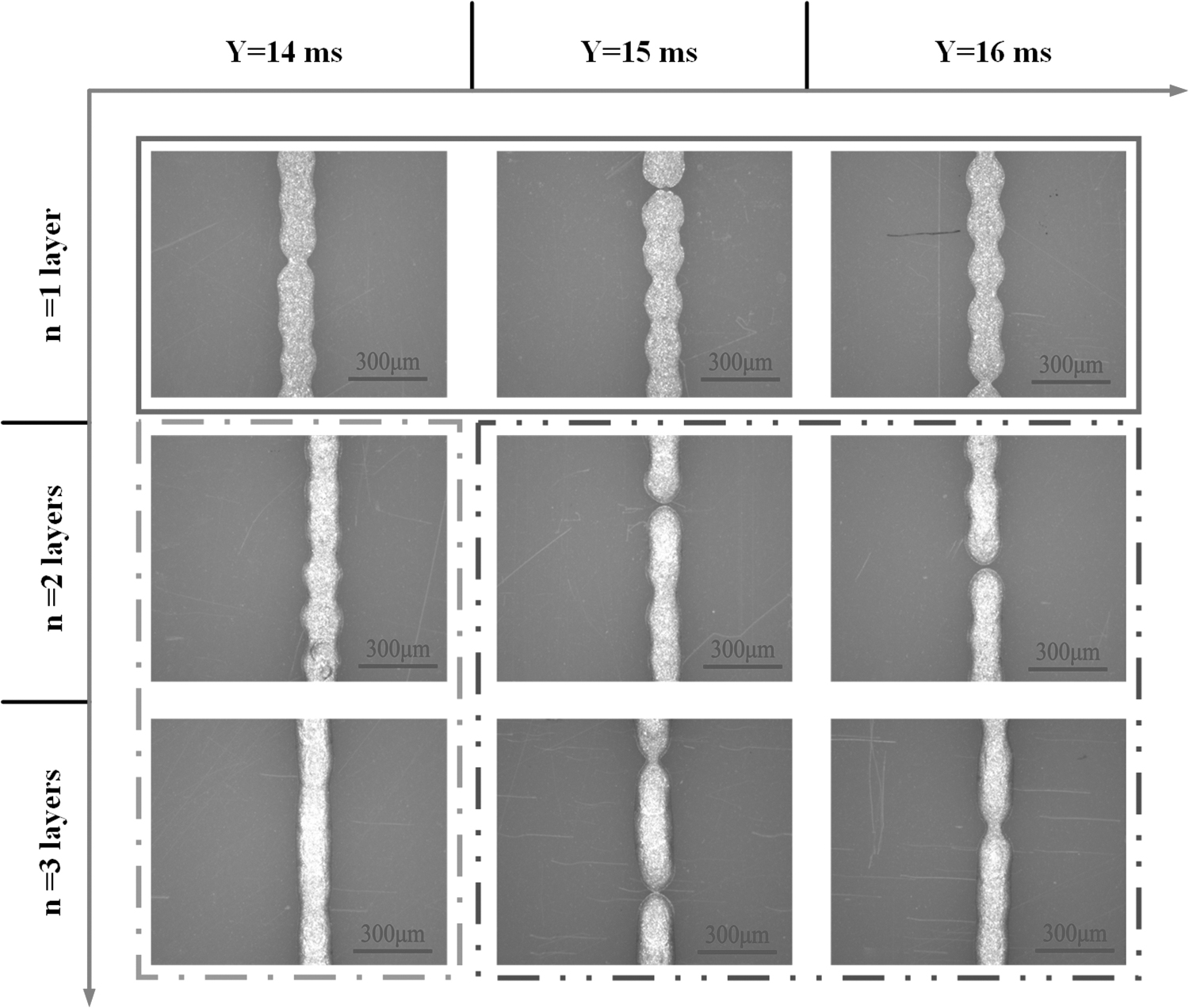
The images with a magnification of 400 × for observing continuity of conductive lines at the printing speed of 1600 mm/min when the platform temperature is at 60°C. n, number of layers; Y, delay time.
According to the experimental investigation, the delay time of no <5 ms and the minimum printing speed of 800 mm/min were identified to print continuous lines. Moreover, the platform temperature should be set below 70°C. This is because the curing temperature of the ink is 80°C and a platform temperature varying from 70°C to 80°C will place the ink into a semicured state, which hinders drops extending on substrate. Simultaneously, it cannot precure silver ink on substrate during printing process when setting the curing temperature (below 50°C). Finally, the selected process parameters and their levels for the full factorial design of experiments are determined as shown in Table 3.
The Process Parameters and Their Levels of Inkjet Printing Conductive Lines
The establishment of model for quality prediction of conductive lines
With obtained data from experiments, the width, thickness, and resistance of the conductive lines can be modeled with the help of artificial neural networks (ANNs). The structure of the ANN is shown in Figure 5. It uses a typical 3-layer network model, consisting of input layer, single-hidden layer, and output layer. It can approximate any non-linear function using the 3-layer network. The input layer contains four input nodes and the corresponding input variables are platform temperature, printing speed, number of layers, and delay time. The hidden layer adopts the S transmission function tansing including n neurons. The relationship between the number of neurons in different layers is determined according to the following experienced formula 38 :
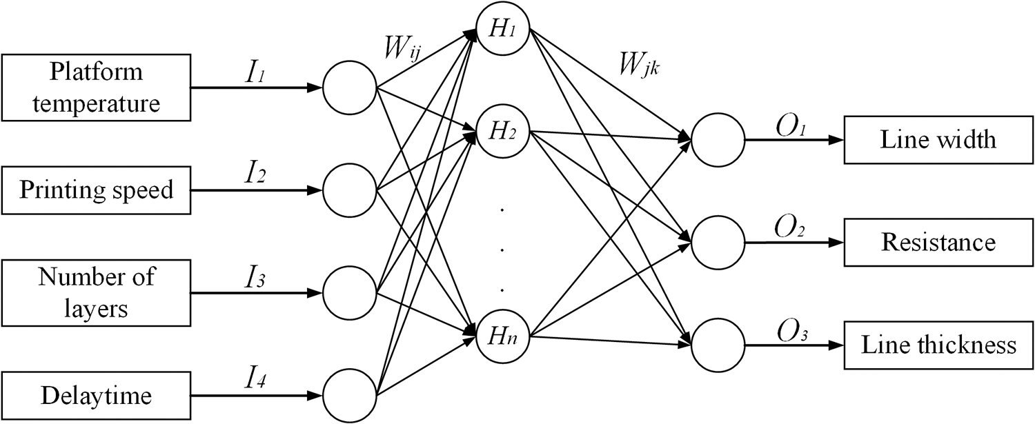
The structure of the artificial neural network.
where a is the constant within the range of [0, 10], M, n, and m are the number of neurons in the hidden layer, input layer, and output layers, respectively.
The output layer adopts a linear transmission function purelin as activated function, which contains three nodes O1, O2, and O3 corresponding to the line width, resistance and line thickness, respectively. As demonstrated in the Figure 5, W ij represents the weight value connecting the input layer node i with the hidden layer node j. Wjk represents the weight value connecting the hidden layer node j with the output layer node k. Where i = 1, 2, 3, 4; j = 1, 2, …n; k = 1, 2, 3. Table 4 shows the fixed model parameters in detail.
The Selected Parameters of Artificial Neural Network Model
ANN can adjust the parameters without constraints with the ability of fitting 100% of the sample. However, overfitting models can only get better prediction results in the training sample and cannot be verified in other samples. The K-folding verification is randomly divided into k groups. First, one group of data is selected as test data and the remaining k–1 groups are used as training data. Then, the other parts are chosen as a new test set, repeating the k times and finally get the average accuracy of the k times (as shown in Fig. 6). In this article, the 50 group sample data are used to further verify performance of the model and then divide the remaining 575 sets of data into 5 folds, which include 115 groups data per fold.
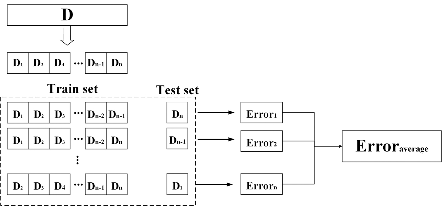
The K-fold crossvalidation.
In the training model, the 4 folds are used as a training set for training models and the remaining fold is used as a test set to evaluate the accuracy of the trained model. Using different division methods, the ANN model can be trained multiple times so that the predicted model with the smallest error can be obtained. This study adopts the crossverification method at k = 5 to avoid the occurrence of overfitting so that the model can find objective laws instead of simply retrieving samples.
For eliminating the effect caused by the different amounts of the input parameters, it should unify all input parameters to [0, 1]:
where i represents the serial number of the input parameter (1 ≤ i ≤ 4), and j represents the serial number of the samples (1 ≤ j ≤ 625). Xij refers to the value of ith parameter in jth sample. Xi,min is the minimum value of ith parameter and Xi,max is described as the maximum value of ith parameter.
To qualify the predicted accuracy of the established ANN model, the article introduced the relative error ɛ, which reflects the actual gap of the predicted value deviating from the measured value. The calculated formula is as follows:
where h is the predicted value in sample set and y refers to the measured value of the sample set. The smaller the ɛ, the higher the credibility of the predicted models.
Finally, the introduction of linear model and linear model with interactive effect are compared with the ANN model. The training process is run based on the MATLAB version R2022a. The hardware tool for training of the ANN is based on AMD Ryzen 7 5800H with Radeon Graphics 3.20 GHz. As shown in Figure 7, the test set begins to enter the converged state and no fluctuation has taken place before searching the optimal solution when the number of iterations is greater than 100 (>100). In the real operating process, the test set could consume near 5 ms after completing an iteration calculation. Finally, the mean square error of the trained model stabilizes at the iterations of 480.

The converged cure between train set and test set.
Results
In this part, the line width, resistance, and line thickness were assessed against process parameters using main effect plots, followed by the analysis of interactive effect of process parameters on the quality of conductive lines and the prediction of line width, resistance, and line thickness using ANN. Based on the obtained results, the optimal combination of process parameters to fabricate lines with small width, uniform thickness, and low resistance are identified.
Main effect analysis on quality of conductive lines
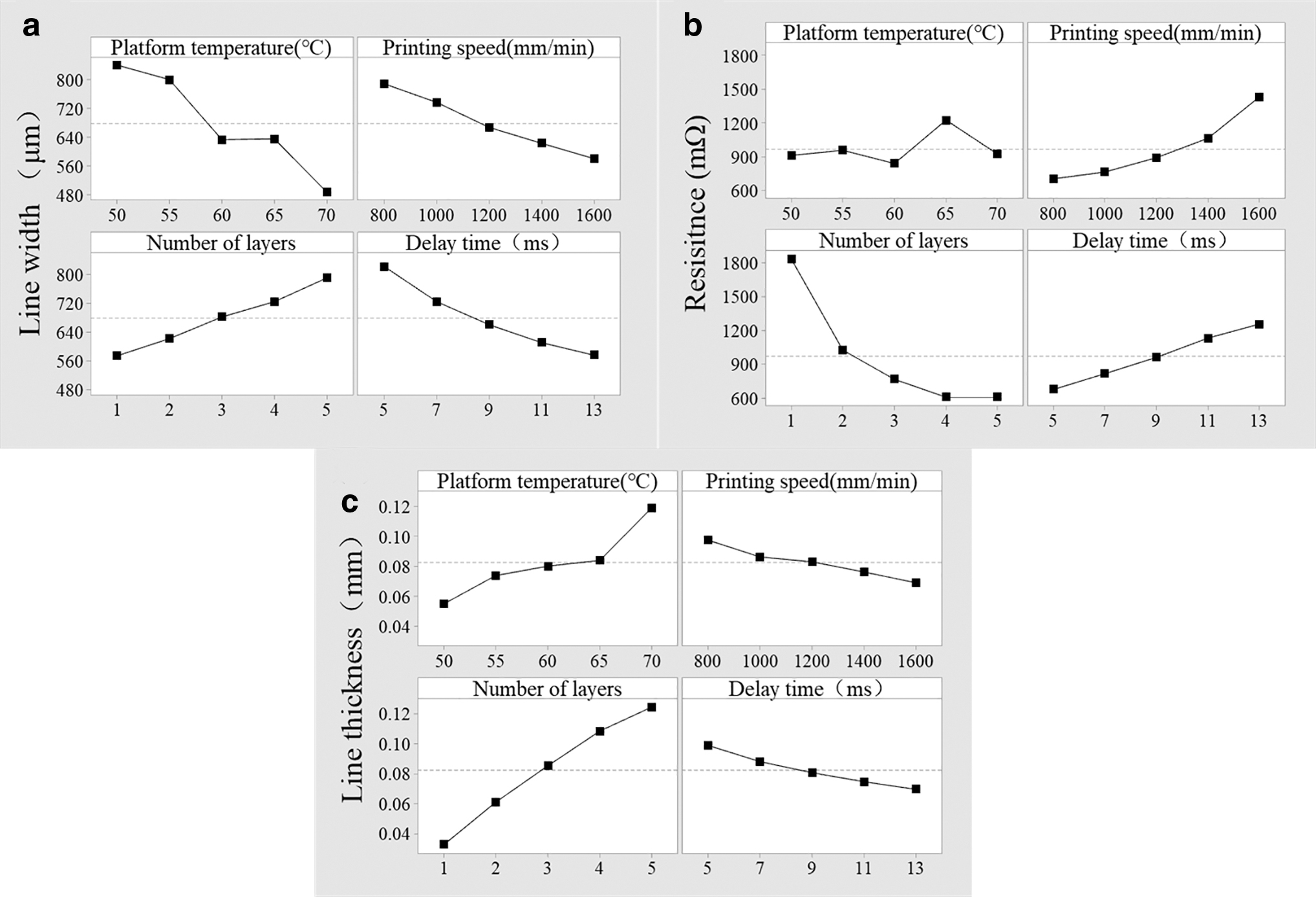
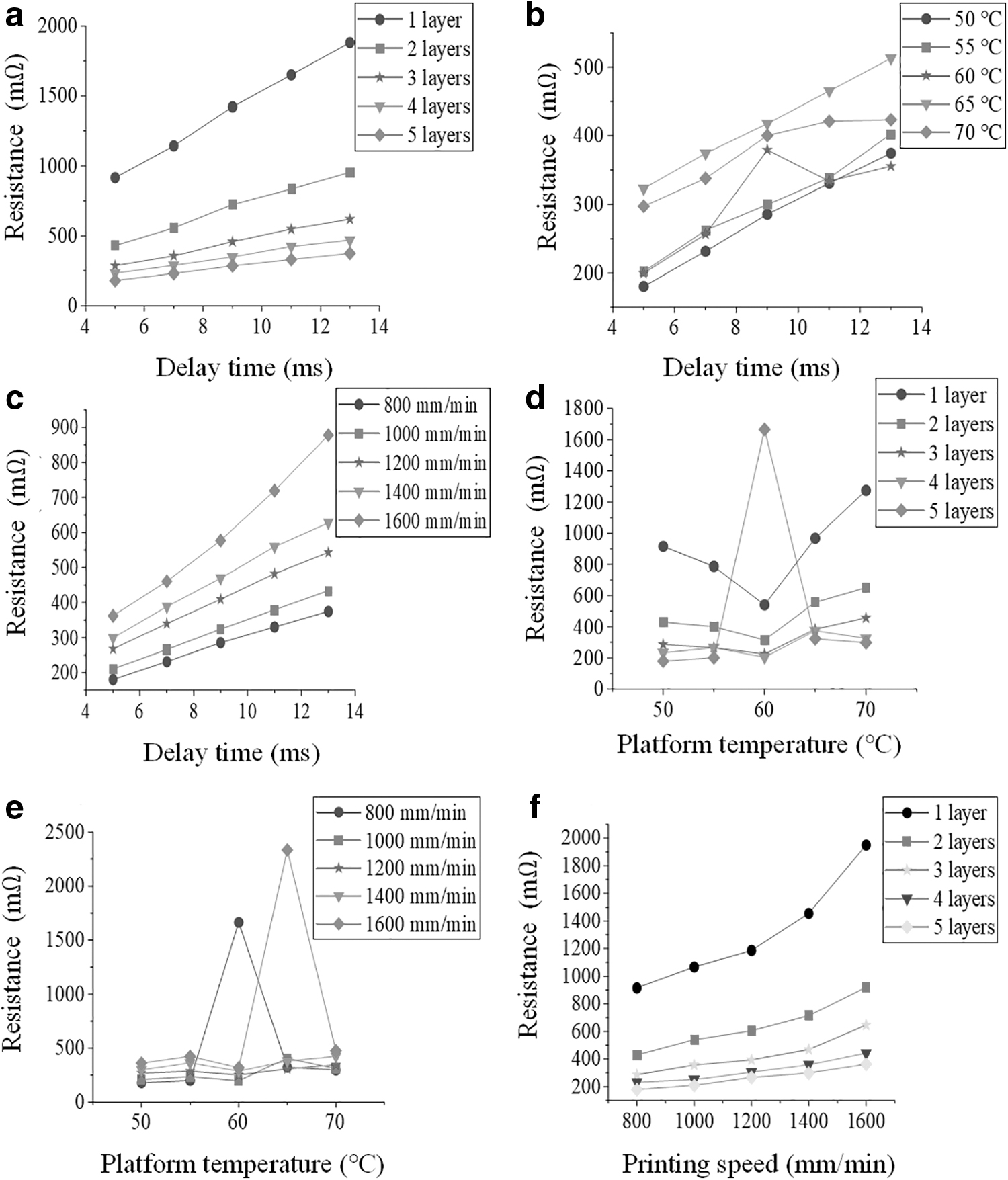
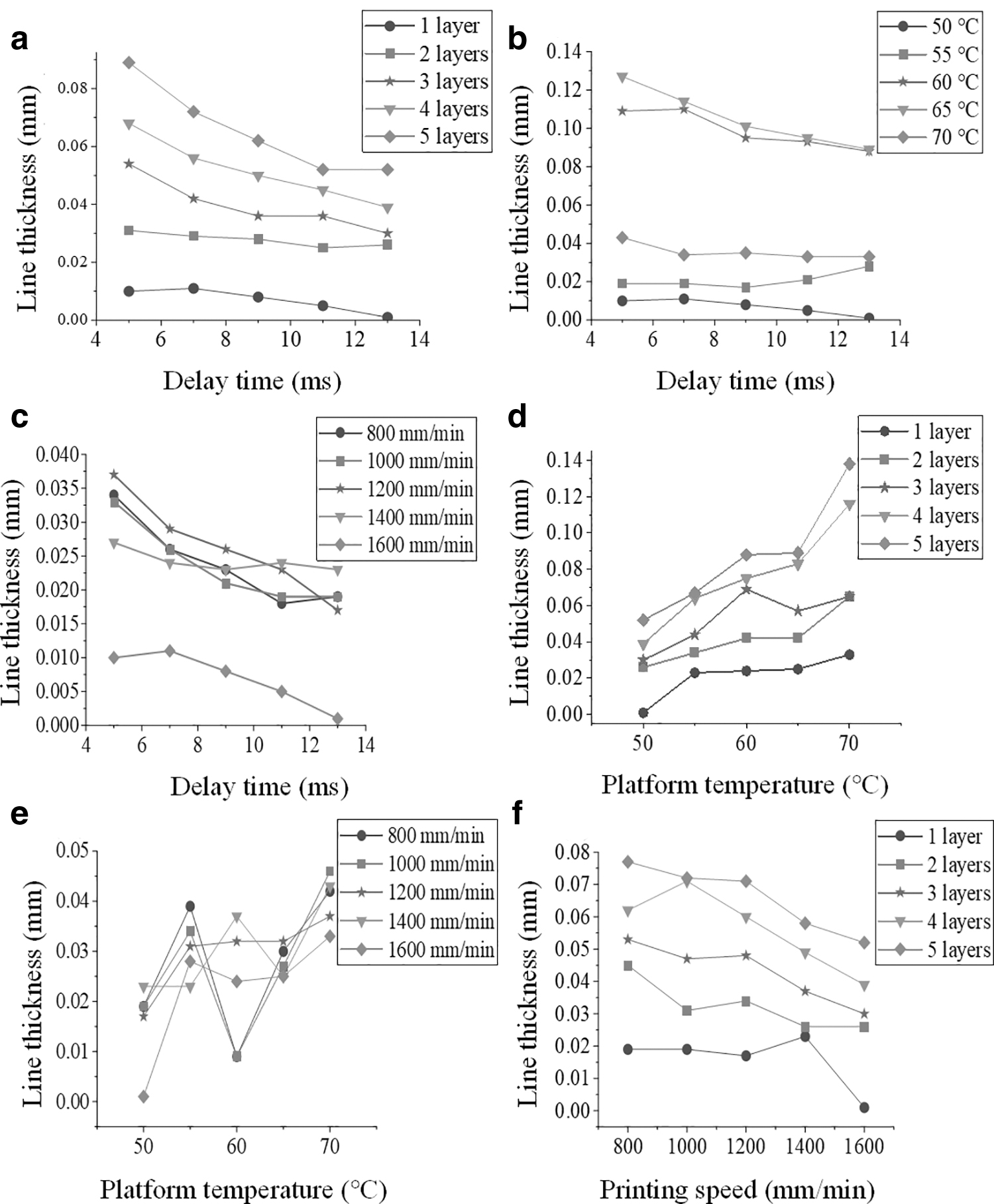
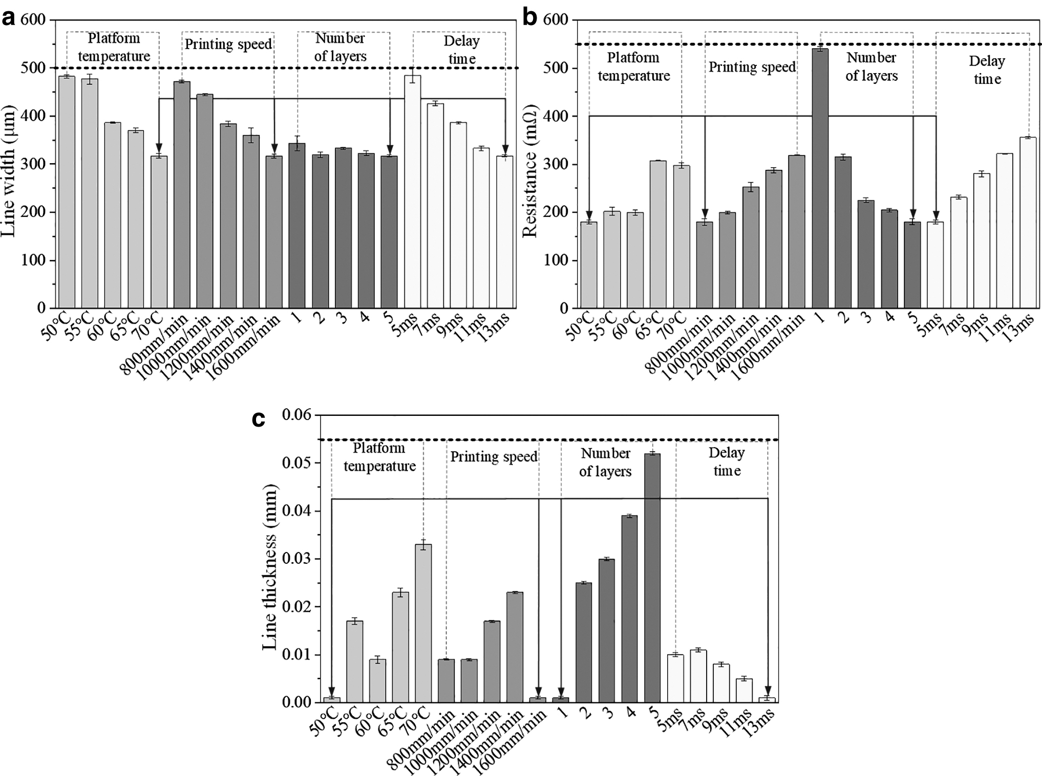
The effects of process parameters on line size (width and thickness) and resistance are investigated, as shown in Figure 8. Line width decreases with an increased printing speed, an increased delay time, and decreased number of layers. In addition, the line width also decreases with an increased platform temperature with the exception that the platform temperature increases from 60°C to 65°C. The resistance is significantly affected by printing speed, number of layers, and delay time, which decreases with an increase of number of layers and increases with an increase of printing speed and delay time. The variation of platform temperature has little effect on resistance, except for a platform temperature of 65°C. A reduction in the number of layers and an increase in the printing speed increase the distance between adjacent droplets delivered into the substrate. As a result, the quantity of droplets decreases, which will lead to a decrease of line conductivity. It is also noticed that the line thickness increases with an increase of platform temperature and number of layers and decreases with an increase of printing speed and delay time.
Main effect plots of platform temperature, printing speed, number of layers, and delay time for:
The platform temperature exhibits the opposite effect on the variation of line width and line thickness. In conclusion, a lower printing speed and delay time coupled with a higher number of layers can result in a large line width and line thickness without considering the platform temperature. A higher printing speed and delay time will lead to an increase in resistance at the same number of layers. Therefore, the high printing speed, delay time, and low number of layers are recommended to fabricate line with small width without scarifying conductivity to improve the integrated level of circuits and alleviate the difficulty of packaging.
Joint analysis and prediction on line width
To investigate the interactive effect among process parameters on the variation of line width, resistance, and line thickness, the joint analysis is conducted by varying the two different process parameters and keeping the third parameter and fourth parameter at the constant level.
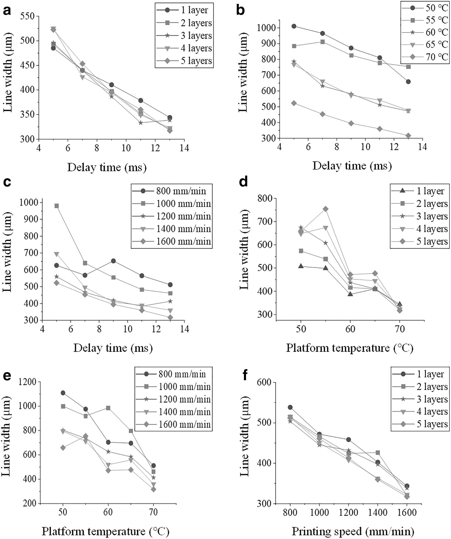
Figure 9a shows the variation of line width with increasing number of layers and delay time when the platform is heating up to 70°C and moving at the speed of 1600 mm/min. An increased delay time from 5 to 13 ms can result in a decrease to almost half of the initial width at 5 ms, whereas the line width does not change significantly in the same level of delay time with the number of layers varying from 1 to 5 layers. It can be speculated that the deposited droplet at 70°C immediately precure and does not spread on the substrate. When the printing speed is 1600 mm/min and printed layers is 5, the line width hardly changes by varying the platform temperature from 60°C to 65°C or from 50°C to 55°C, as shown in Figure 9b. Nevertheless, the relatively small line width (317.265 μm) is obtained when the platform is heated to 70°C and the delay time is selected as 13 ms. As seen from Figure 9c, by increasing printing speed and delay time, the line width decreases except for that at 800 mm/min. The low level of printing speed influences line width irregularly.
The variation of line width with different combination of process parameters:
The reason is that the jetting frequency of droplets will decrease with increased delay time, then the droplets' spacing will expand with an increase of printing speed, and eventually the combined effects will result in the reduced line width. Figure 9d describes that the line width increases and then decreases periodically when the number of layers and delay time increases. Furthermore, the line width will have small variation in the same level of delay time with increased number of layers and platform temperature. As shown in Figure 9e, the final line width will decrease with the increased platform temperature and printing speed, whereas, the line width varies irregularly at different levels of platform temperature. The final line width decreases with the increased printing speed and the number of layers.
By comparing Figure 9a with Figure 9f, it is found that the number of layers and the delay time, or the printing speed will exhibit similar effect on the variation of line width. Therefore, the interactive effect of the delay time and the number of layers on line width exhibits the similar trends as that between the printing speed and the number of layers. In addition, their interactive effect on line width is more obvious than that of other parameter interactions.
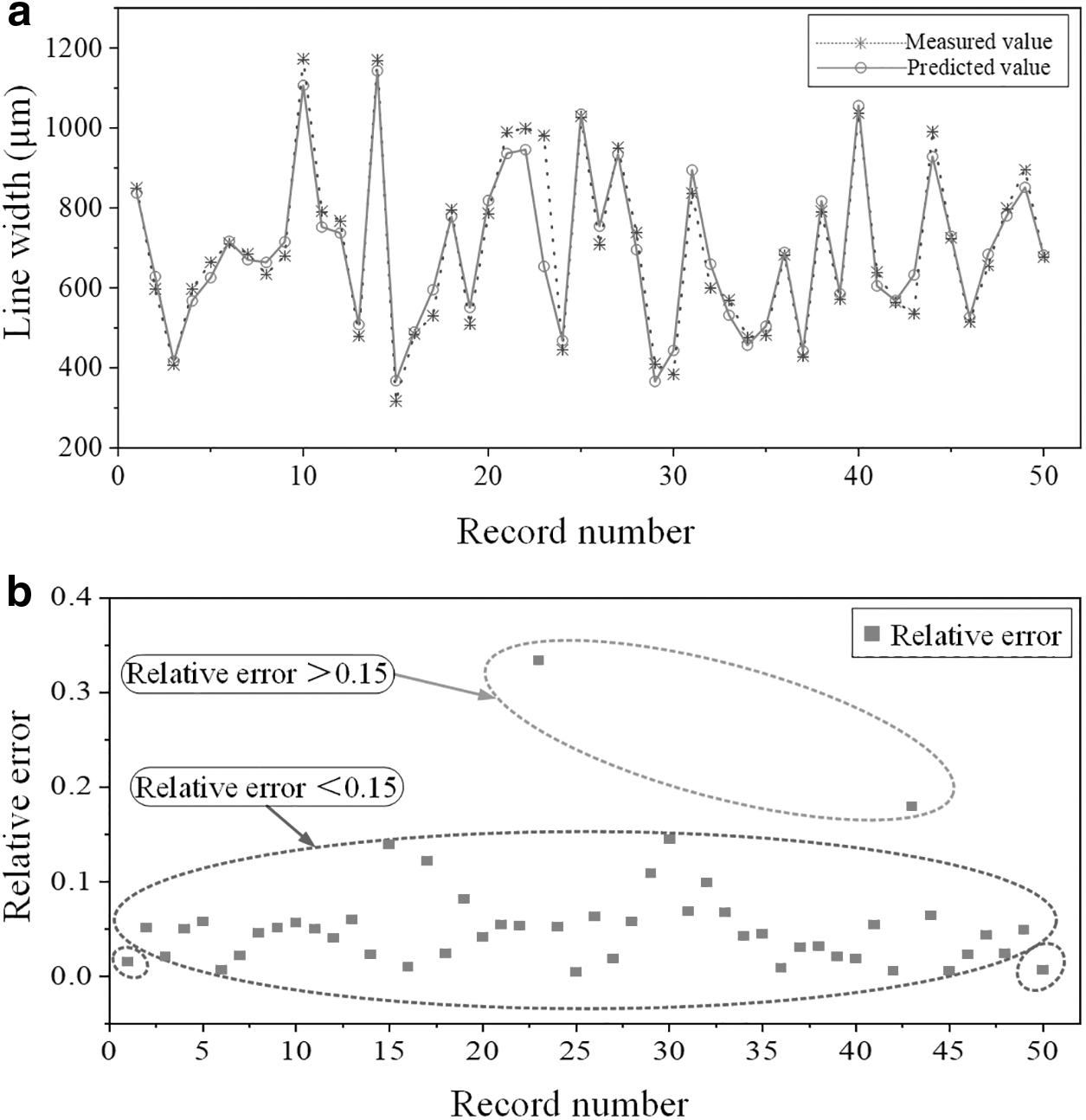
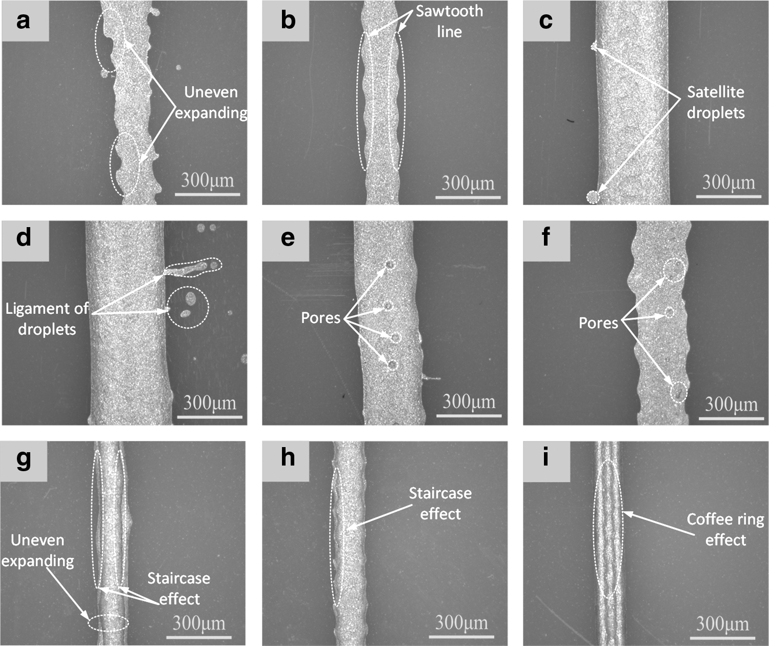
Based on the above experimental data, a predicted model is established and its accuracy is verified. As shown in Figure 10a, it exhibits the comparison between the predicted value and measured value for line width using ANN. By encoding the validation set data, it is seen that the relative error is in a reasonable range [0, 0.15] except for the No.23 and No.43. It is mainly caused by the uneven heating as it stops extension rate of the droplets. Finally, the random extending of droplets on the substrate will happen as shown in Figure 11a. The model effectiveness of predicted line width within [0, 0.15] is 96%. It can be seen from Figure 11b that the sawtooth-shaped line will also affect the variation of line width. As an evaluated index, the results elucidate that the R2 for the linear model, linear model with interactive effect, and ANN model are 0.84, 0.89, and 0.91, respectively. It is concluded that the process parameters have interactive effects on line width, which is consistent with joint analysis on line width, as displayed in Figure 9. The linear model is unsuitable for performing the regressive analysis even if incorporating an interactive effect.
The predicted results for line width using artificial neural network:
The external morphology of conductive lines in different recorded number:
The obtained line width with desired edge using a single-factor analysis method is not convincing. 30 The process parameters affecting the line width based on the following order are: number of layers > delay time > printing speed > platform temperature according to Table 5.
The Analysis of Variance for Nano-Silver Line Quality in Four Variables
Calculation error of contribution percentage: ±1%.
A, platform temperature; B, printing speed; C, number of layers; D, delay time; LR, line resistance; LT, line thickness; LW, line width.
Joint analysis and prediction on resistance
As shown in Figure 12a, the low resistance will be obtained based on the increased number of layers and decreased delay time. Specifically, except for printing 1 layer, the resistance of the lines varying from 2 to 4 layers is relatively changing indistinctively (comparing with 1 layer) with increased delay time. These results demonstrate that previous printed layers have a strong impact on drop coalescence and imbibition. Simple droplet or single layer of conductive lines are not beneficial for improving conductivity. When the printing speed is kept at 800 mm/min and the number of printing layers is 5, the resistance will increase with increased delay time and platform temperature, except for delay time varying from 7 to 9 ms at 60°C, as shown in Figure 12b. However, the resistance will increase with an increase of delay time and printing speed in Figure 12c.
The variation of resistance with different combination of process parameters:
In addition, it is uneconomical to decrease resistance through increasing number of layers and printing one layer is inadvisable for gaining the desired conductivity, because resistance is 2–3 orders of magnitude higher than that when printing 2–5 layers, except for printing 5 layers at platform temperature of 60°C in Figure 12d. Figure 12e shows that the resistance has a subtle variation with an increase of delay time and an increased printing speed from 1000 to 1400 mm/min.
It is found that the low or high printing speed significantly affects the resistance while other levels of platform temperature hardly affect it. According to the laws of resistance, the resistance of the line is proportional to its length and inversely proportional to its cross-sectional area. The increasing printing speed will enlarge droplet spacing. At the same time, an increased platform temperature will prevent the droplets expansion. Finally, the small cross-sectional area of printed lines will be generated leading to an increased resistance. It should be noted that the resistance has a sharp increasing at the printing speed of 800 and 1600 mm/min when the platform temperature ranges from 55°C to 60°C and from 60°C to 65°C, respectively. Figure 12f shows that the interaction between the number of layers and printing speed on resistance represents the same varied trend as Figure 12a. In short, the resistance is greatly influenced by the printing speed and number of layers (mainly aim at 1-layer and 2-layer conductive lines), and it is significant to select them appropriately.
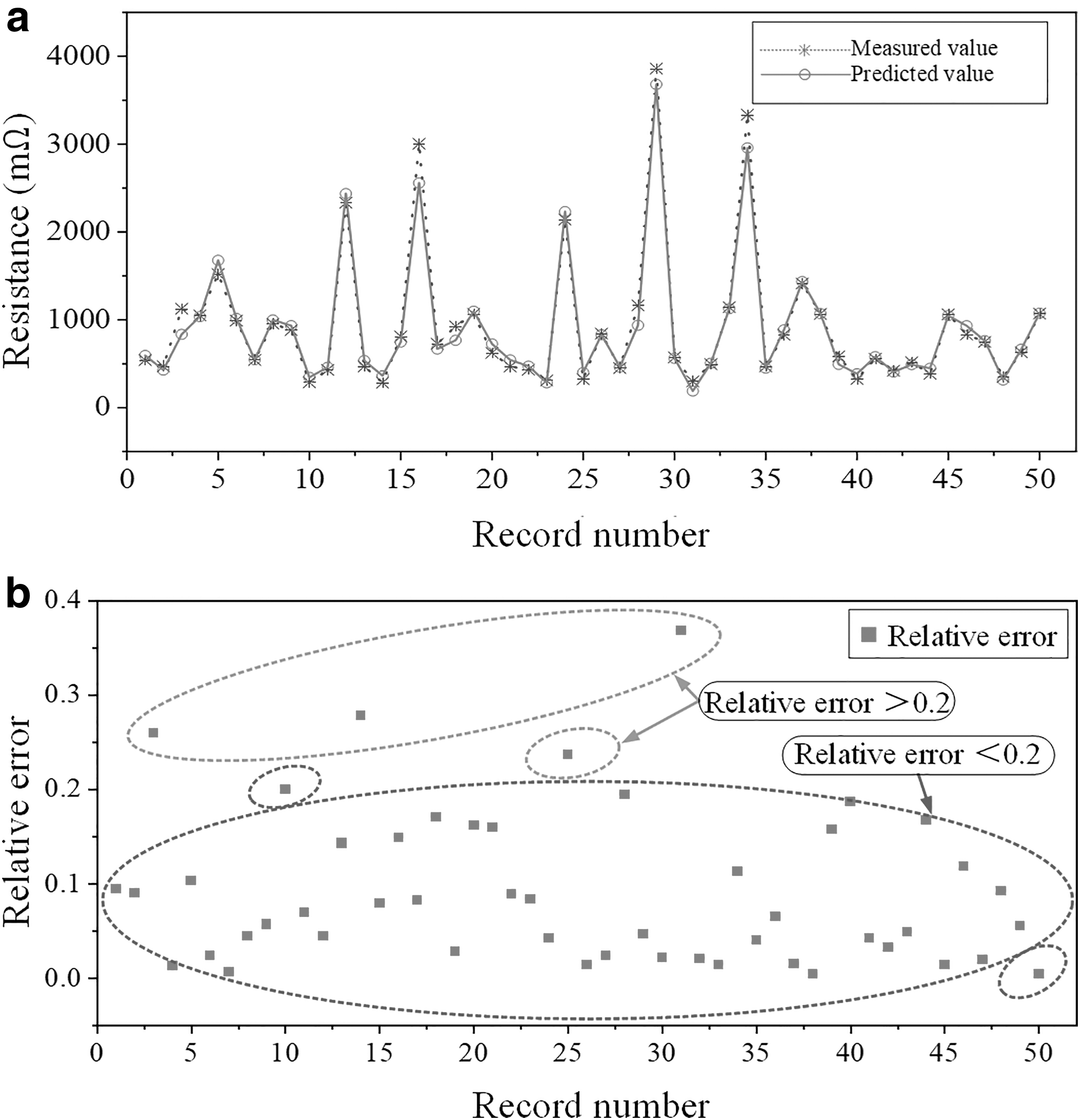
In this section, the resistance for conductive lines is predicted by ANN, as described in Figure 13a. The overall predicted accuracy is presented in a controllable range [0, 0.2] except for No.3, No.14, No.25, and No.31, as shown in Figure 13b. The corresponding external outline of conductive lines is represented as in Figure 11c–f, respectively. The reason is that the satellite droplets and ligament of droplets produced by lines of No.3 and No.14 are scattered at substrate randomly that affects the normal current passing in Figure 11c and d, respectively, which causes an increase of resistance sharply. The resistance for the line No.25 and No.31 also will increase due to the conductive lines with large pores after drying nano-sliver ink, as illustrated in Figure 11e and f. The model effectiveness of predicted resistance within [0, 0.2] is 92%. Based on built regressive models for the resistance, the R2 of linear model, linear model with interactive effects and ANN model are 0.59, 0.64, and 0.96, respectively.
The predicted results for resistance using artificial neural network:
Furthermore, the interactive effect between the process parameters on resistance exists due to internal-evolved mechanism in adjacent deposited droplets. The linear model has no ability to predict the resistance of conductive lines in comparison with ANN. As presented in Table 5, the influence of process parameters on resistance is based on the following order: the number of layers > printing speed > delay time > platform temperature.
Joint analysis and prediction on line thickness
As shown in Figure 14a, the line thickness is significantly affected by the number of layers while the delay time has little effect on it. This is because the influence of the drop spacing brought from delay time is far less than that caused by line thickness variation when increasing the number of layers. In Figure 14b, the higher line thickness can be achieved at the platform temperature of 65°C and at the delay time of 5 ms. Increasing the platform temperature from 60°C to 65°C will have little effect on variation of line thickness. Figure 14c depicts that the printing speed of 1600 mm/min can reach the maximum line thickness of nearly 0.01 mm at 7 ms, whereas other level of printing speed has obvious effect on the line thickness with an increased delay time from 5 to 13 ms, except for setting up the printing speed of 1400 mm/min. It is reasoned that a higher printing speed influences the flight path and shape of ejected droplets from the nozzle before droplets reach the substrate. Except for the platform temperature varying from 55°C to 65°C, line thickness increases a lot by increasing other levels of platform temperature and number of layers, as seen from Figure 14d.
The variation of line thickness with different combination of process parameters:
As shown in Figure 14e, upon increasing the platform temperature from 50°C to 70°C and decreasing printing speed from 1000 to 800 mm/min, the values of line thickness fluctuate up and down. Take it a step further, it increases with increasing the platform temperature from 50°C to 55°C, and declines with an increased platform temperature from 55°C to 60°C and grows as adding up the platform temperature from 60°C to 70°C in the end. However, the printing speed of 1400 mm/min exhibits the opposite effect on the line thickness, except for the increase of platform temperature changing from 50°C to 55°C and from 65°C to 70°C. In addition, selecting the printing speed at 1200 and 1600 mm/min presents similar effect on the line thickness. As demonstrated in Figure 14f, it is noticed that line thickness decreases by increasing printing speed and number of layers. Such trends are the same with those of line thickness as described by Figure 14a. To sum up, the number of layers and the platform temperature are the pivotal factors in determining the line thickness.
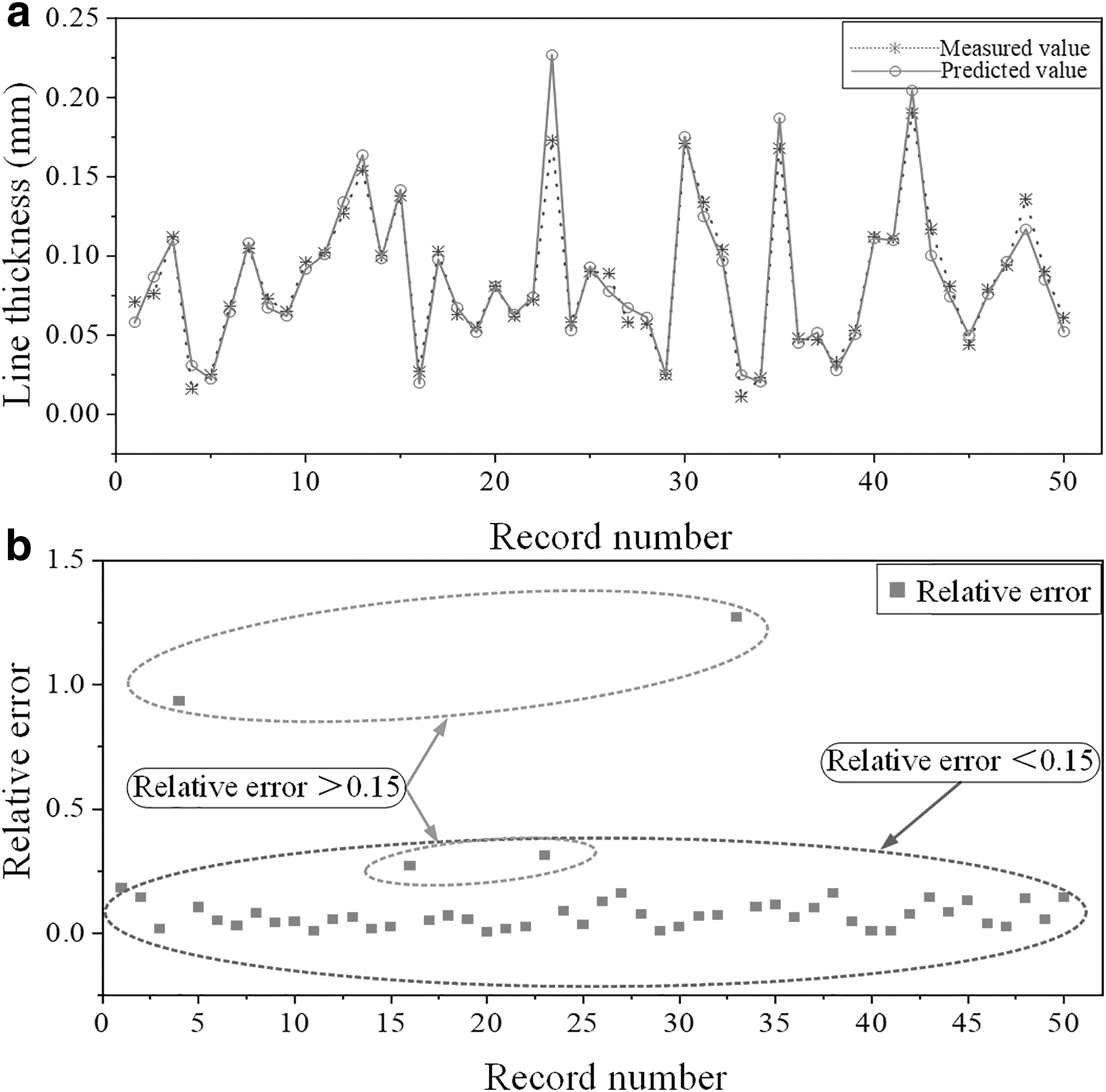
Figure 15a shows the variation of line thickness of 50 lines between the predicted and measured value. The predicted accuracy of lines No.4, No.16, No.23, and No.33 are lower in comparison with other conductive lines within the relative error of [0, 0.15] in terms of line thickness, as plotted in Figure 15b. The line No.4 and No.16 are mainly caused by staircase effect during multilayer printing, which leads to nonnegligible effect on line thickness during measuring process, as shown in Figure 11g and h. On the contrary, the line No.23 is generated due to the droplets expanding unevenly during the single layer printing process. Multilayer printing of conductive lines indicates that the interaction between newly arriving droplets and previously existed droplets may play a crucial role in preventing balling and bulging of lines. Hence, the line thickness varies irregularly in the total length, as shown in Figure 11a. The line No.33 (ɛ = 127.2%) may be caused by the choice of measured position under condition of uneven heating. Specifically, Figure 11i displays the peaks at two sides and a valley in the middle, which is called the coffee ring effect.
The predicted results for line thickness using artificial neural network:
The nanoparticles of silver ink mainly accumulate at the air/liquid interface instead of the interior when droplet dries rapidly. The deposited droplets at the margin of printed line dries faster than that in the center position as the edge has a smaller quantity of liquid than that in the center. The above phenomenon indicates that the obtained data will be an outlier value no matter the peaks or a valley is identified as a measured value. Thus, the predicted accuracy of model will be vastly influenced. Totally, the model effectiveness of predicted line thickness within [0, 0.15] is 92%. The goodness of fit of linear model, linear model with interactions, and ANN model are 0.85, 0.90, and 0.95, respectively. The three models show high prediction accuracy, whereas the ANN presents the most desired performance. The influence of process parameters on line thickness is based on the following order: platform temperature > delay time > number of layers = printing speed, as shown in Table 5.
The selection of combined process parameters applied in integrated electronics
Figure 16 shows line width, resistance, and line thickness of AM printed lines for different jetting alignment parameters. The minimum line width is 317.265 μm by printing 5 layers when setting the platform temperature of 70°C and printing speed of 1600 mm/min while maintaining the delay time of 13 ms. Furthermore, the number of layers should be minimized under the condition of high-density interconnection, as shown in Figure 16a. It can be noticed that the minimum resistance and thickness of printed lines are 180.5 mΩ and 0.001 mm corresponding to the combination of process parameters (50°C, 800 mm/min, 5 layers, and 5 ms) and (50°C, 1600 mm/min, 1 layer, and 13 ms), respectively, as shown in Figure 16b and c. It can be seen from Figure 16 that the upper limit of minimum line width, resistance, and line thickness are below the 500 μm, 600 mΩ, and 0.06 mm (marked with blue dotted line) under different jetting alignment parameters, respectively. For better characterization of width and thickness of printed lines, the aspect ratio δ of the silver lines is introduced to evaluate the morphology of conductive lines in Eq. 4:
The minimum characterized response of conductive lines printed using different jetting alignment parameters:
where H is the line thickness and W is line width (the units of line width and line thickness need to be unified before calculating).
In integrated electric fields, the printed line width should be minimized without sacrificing conductivity. In other words, the δ should take a high value as much as possible. A multiobjective optimization is normally adopted in achieving the low resistance and relatively high aspect ratio simultaneously using Minitab version 2019. Therefore, the optimized parameter configurations are as follows: platform temperature: 70°C; printing speed: 1139.39 mm/min; number of layers: 5; and delay time 12.20 ms with the desirability of 0.851 to achieve the goal of minimum resistance in addition to maximize the
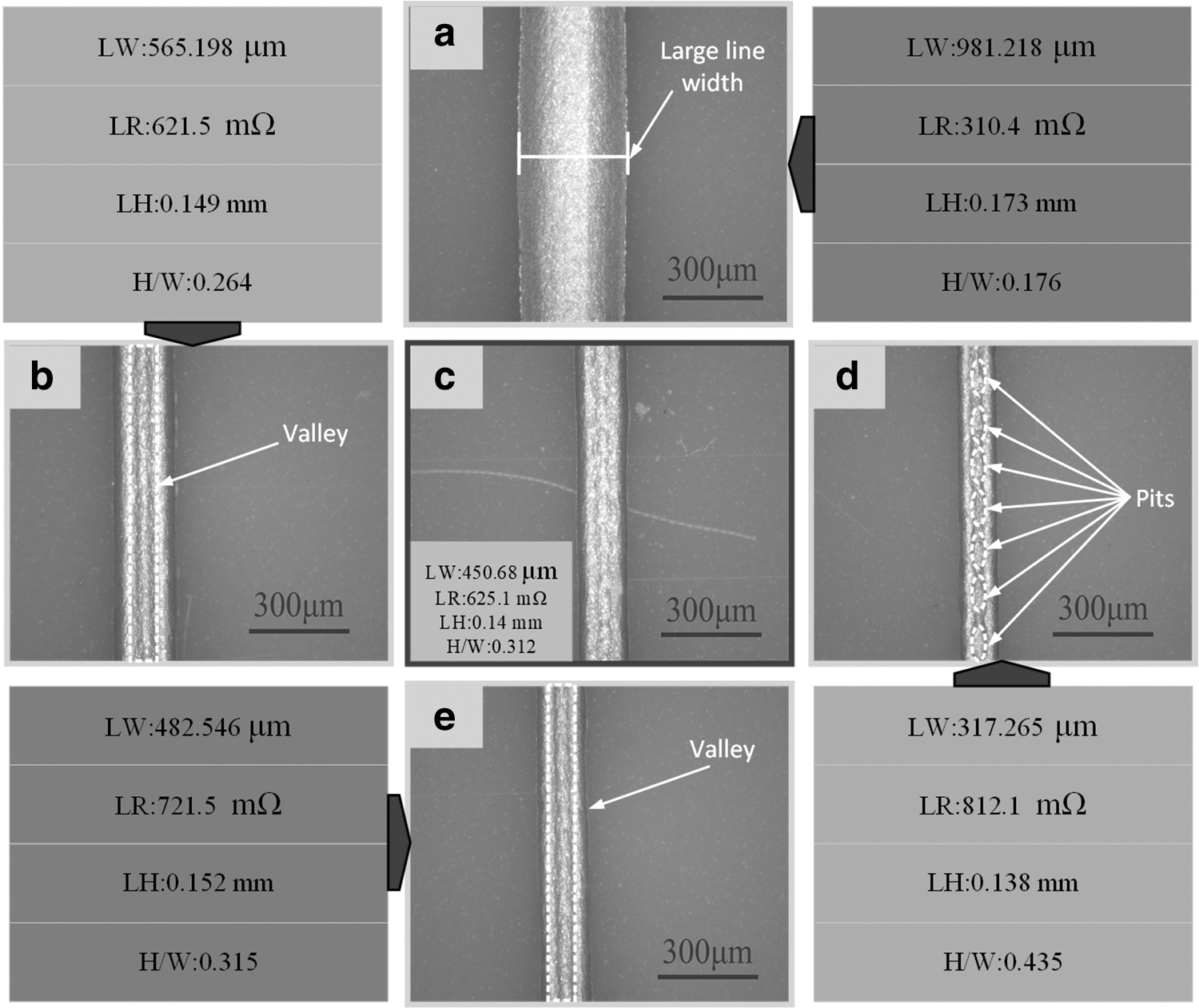
Morphology of the conductive line at 70°C when printing 5 layers:
The Desirability Criteria of Process Parameters and Targeted Responses
δ, aspect ratio.
Comparison Between the Predicted Data and the Experimental Data of Nano-Silver Lines
However, the LR and H/W in Figure 17a are very low value and the valley is created in Figure 17e. From the prospective of printing speed, Figure 17b and d generates valley and pits on the lines surface, respectively. In parallel, the LR and H/W are not desired as Figure 17c. In addition, the various indices of printed lines in Figure 17c are within the required scope of Figure 16.
Discussions
Conductive ink and functional components are the research priorities in existing MAM studies, especially for IJP, whereas the study on conductive line formation is lacking. Conductive lines are basic channels to connect the electronic components. As continuity of lines is a prerequisite, line width and line thickness cannot stand alone in achieving desired conductivity. The biggest advantage of IJP is that the manufacturing for customized electronic devices has been achieved without limitations of dielectric substrates. The line width will decrease greatly with increasing the number of layers, 39 which is in line with this work.
For the interactive effect among process parameters on conductive lines, the contribution percentage of process parameters on the targeted responses is also discussed. In general, the contribution percentage on targeted responses are calculated based on the ratio of the overall adjusted sum of squares and the individual adjusted sum of squares. The detailed contribution percentage results for Linear (A, B, C, and D), two-way interaction (A × B, A × C, A × D, B × C, B × D, and C × D), and Square (A × A, B × B, C × C, and D × D) are shown in Table 5. It is noticed that the interactions between the number of layers and the platform temperature have a tremendous contribution to the line width and line thickness of silver lines with 32.958% and 46.868%, respectively. It is reasoned that the platform temperature can reduce line width through enhancing the surface tension of droplets and precuring silver ink. On the contrary, the additional layers can increase the line width based on superimposed effect.
As shown in Figure 9d, an increased number of layers has a slight effect on the line width when the platform temperature is at 70°C. As for line thickness, the multilayer line has a valley in the middle and peaks at both sides (as shown in Fig. 17b, e) at 70°C as opposed to the one-layer line, and the coffee ring effect has diminished (as shown in Figs. 3 and 4). It is deduced that the previous layer is not fully cured when the additional layer is persistently deposited. The nonevaporated solvent could drive the agglomeration of nano-silver particles near the line edge at both sides.
30
Finally, the electrical behavior of conductive tracks in terms of resistivity is intensively focused on.
40
The resistance of IJPed conductive lines is determined using the Eq. 5:
where R is resistance, ρ is resistivity, L is length of conductive lines, and A is cross-sectional area of conductive lines. The main significant contribution percentages for resistance are the square of number of layers with 46.928%. According to Eq. 5, the interactive effect between the number of layers can tremendously decrease resistance through reducing the effective area of conductive track (
Line formation (the ability for droplets to coalesce into a continuous line) depends on droplet size and droplet interarrival time.42,43 According to Table 5, the delay time has a contribution to the line width with 11.429%. It is mainly reasoned that the line width changes with the ejection frequency of droplet controlled by delay time. Furthermore, the interaction of number of layers and printing speed, the interactive effect between number of layers and delay time have a contribution on resistance and line thickness within the near range of 10–15%. Specifically, the increased printing speed and delay time have a negative effect on the resistance and line thickness and vice versa for an increased number of layers. Therefore, the optimization of printing speed and delay time in Section “The selection of combined process parameters applied in integrated electronics” is of significant importance.
There is a growing recognition that the discontinuous printed lines will directly affect the conductivity, and the large pores and long valleys are difficult to eliminate after drying the solvent completely as shown in Figure 11e and f. For this reason, the sharp increase in resistance is unavoidable. Therefore, the effectiveness of the ANN model for resistance (92%) within the relative error of [0, 0.2] will be relatively lower in comparison with line width (96%) and line thickness (92%) within the relative error of [0, 0.15], as described in Figures 10b, 13b, and 15b.
In addition, printing one-layer conductive line is rougher than the substrate due to strong droplet flow on the heterogeneous substrate. The manufacturing of an ideal printed line should be real-time monitored. Only the previous layer is commendably printed; the next layer can be well adhered in manufacturing of the high-performance conductive lines. Otherwise, the staircase effect and trench phenomenon will occur as in Figure 11h and i. Ultimately, the short-circuit phenomenon and undesired interconnection between conductive lines (such as bulging line, scalloped line, and no line [pairwise beads or isolated drops])44,45 will destroy electrical components in the domain of integrated industries.
Limitations and Future Work
This article proves potential superiority in the quality prediction of IJPed conductive lines through ANN model, but does not establish a data-driven model to achieve accurate control of line width, resistance, and line thickness through adjusting process parameters with an aim to reduce experimental workload. In the subsequent research, a diverse range of line width, line thickness, and line resistance will be determined in facing diverse engineering applications using data interaction model. Additionally, the geometrical parameters, such as the nozzle diameter and the standoff distance between nozzle and substrate, should be controlled to reduce satellite and ligaments of droplets in forming lines. Also, the testing of mechanical properties, including flexibility, ductility, and bending strength, can be utilized to check the robustness of the conductive lines.
In electronical applications, in addition to the line width, resistance and line thickness are studied in this article; other quality indicators also need to be investigated, including the adhesive force between conductive lines and substrates, the surface roughness of printed lines, and other electric properties. Furthermore, the process parameters such as drop extending diameter, the contact angle between the external edge of droplets and the horizontal direction of the substrates, the types of substrate, and curing method need to be investigated.
Conclusions
This study systematically investigates the effect of process parameters on line width, resistance, and line thickness fabricated by IJP process. The article demonstrates the possibility of adopting ANN to predict the quality of conductive lines. The conclusions of this research are summarized as follows:
The process parameters of printing speed ranging from 800 to 1600 mm/min, delay time ranging from 5 to 13 ms and platform temperature ranging from 50°C to 70°C can achieve a good continuity of printed lines used for interconnection electronic. The smaller line width can be printed by the highest level of platform temperature, printing speed, number of layers, and delay time. The resistance decreases with increased number of layers, decreased printing speed, and delay time while the line thickness increases with increased number of layers. The parameter configurations (70°C, 1139.39 mm/min, 5 layers, and 12.2 ms) can be identified to fabricate desired conductive lines used for the integrated circuits. The ANN model can achieve a model effectiveness of more than 90% for line width and line thickness within [0, 0.15], except for the resistance with a model effectiveness of 92% at a greater relative error of [0, 0.2]. The analysis of variance further verifies the conclusion of experimental analysis that there is a highly interactive effect between number of layers and platform temperature on line width and line thickness. However, the interaction between number of layers and other two parameters (printing speed and delay time) mainly affects line resistance. The conductive line with clear edges and smooth surface is prerequisite to ensure the normal conduction. There is a great potential for lowing resistance while reducing defects, such as bulging line and gullying line caused by satellite droplets and nonuniform curing through carefully selecting process parameters in the process design and post-treatment stage.
With the rapid development of microelectronics industries, IJP has attracted extensive attention in interconnecting electronic components due to high design freedom and short process cycle. For designers, the morphology, dimensions, and conductivity of printed line need to be considered simultaneously during the real product design stage. To date, the general relationships between the multivariate operating parameters and formation mechanism of conductive lines are unraveled. The obtained results and the adopted methodology to combine joint analysis and algorithm prediction in this study can be used to assist IJP designers in making a proper decision under facing multiple components' interconnection on substrate using conductive lines.
Footnotes
Authors' Contributions
J.H.: Methodology and funding acquisition. H.Z.: Investigation, and writing—original draft and formal analysis. J.L. and C.L.: Data curation, review and editing (equal). C.C.: Software (lead). Z.Y. and T.P.: Review and editing (equal). J.W.: Validation. L.G.: Funding acquisition. Z.X.: Visualization.
Author Disclosure Statement
The authors declare no conflicts of interest.
Funding Information
This research was funded by Shaanxi Oin Chuangyuan “scientist + engineer” team construction project, grant number 2022KXJ-150, Xi'an Qin Chuangyuan's Innovation-Driven Platform Construction Special Project, grant number 21ZCZZHXJS-QCY6-0013 and the National Natural Science Foundation of China, grant number 51805044.