
Abstract
AlSi10Mg is widely used in additively manufacturing aeronautical lattice and honeycomb structures. The unclear complex quality characteristics has been an obstacle of nondestructive testing of additive manufacturing (AM) AlSi10Mg, especially at its as-built state. This article attempts to reveal the quality characteristics of as-built AM aeronautical AlSi10Mg based on its conductivity characteristics. Experimental results show that the quality of manufacturing is nonuniform. The nonuniformity of each sample surface is systematically evaluated. Along the building direction, the quality is best in the initial few layers and decreases as the built height increases. On this basis, a reference curve is obtained and used to describe the quality characteristics of as-built AM component along the building direction. Based on the quality characteristics, the inspection of small offsets caused by accidental failures during the manufacturing process is carried out. The offsets not <37 μm are detected with the help of the reference curve, whereas they are not discovered by the radiography testing. It proves that the proposed method of offset inspection is highly sensitive.
Introduction
Metal additive manufacturing (AM) uses high-energy beams such as laser or electron beam to melt metal powder or wire and stack them layer by layer guided by digital models.1–3 Selective laser melting (SLM) is one of the most typical AM technologies,4,5 especially in the field of aviation manufacture 6 due to its advantages in manufacturing precise and complex metal components. Aeronautical AlSi10Mg is one of the representative SLM materials in the aerospace industry. For example, aeronautical AlSi10Mg is used for additively manufacturing lattice structure7,8 and honeycomb structure,9,10 for the purpose of structural lightweight and high performance.
AM components often contain defects,11,12 which affect their performance seriously. Measuring conductivity has been an effective nondestructive method for inspecting post-treatment AM components. Lopez et al characterized delamination in post-treatment aluminum and mild-steel specimens by measuring their conductivities. 13 Todorov studied the anisotropy of post-treatment AM sample through measurement of conductivity. 14 Raab et al and Obaton et al used the method of conductivity measurement to detect porosity in AM components.15,16 Boillat et al utilized the method of conductivity measurement to evaluate the mechanical properties of AM components. 17 Kemerling and Ryan, and Singh et al optimized printing parameters by measuring the conductivities of AM components.18,19
Nondestructive inspection of as-built AM components is not found in the literature. It has many advantages to inspect AM components at their as-built state rather than after post-treatment. First, surface finishing process of post-treatment will eliminate or change surface-breaking defect, which is against the optimization of printing process and parameters through nondestructive evaluation. 20 Second, as-built inspection (inspecting at the as-built state) is the basis of online testing that is urgently needed in industry because the printed components at the as-built state retain many properties of the components at the building state. 21 Last but not the least, as-built inspection can avoid post-processing of defective samples and thereby save time, energy, and cost. 22
Reliable as-built inspection of AM components poses many challenges. One of the main difficulties is the unclear complex quality characteristics, which are affected by many factors, such as surface roughness, nonuniformity of microstructure, and irregular stress distribution. Density measurement23,24 and microstructure observation8,25 have been used to assess the quality of as-built AM components. However, the method of measuring density can only obtain the overall quality of the components, and microstructure observation is destructive, expensive, and time-consuming. Some studies17,26,27 used conductivity to characterize the factors affecting the building quality. The method of measuring conductivity can obtain both global and local quality characteristics of components with high efficiency. However, conductivity characteristics of as-built AM components have not been reported. This article investigates the conductivity characteristics of as-built AM aeronautical AlSi10Mg. On this basis, quality characteristics of as-built AM components are obtained.
Many AM metal components such as turbine engine, 28 rocket nozzle, 29 and turbine blade 30 have slanted sidewall geometry features. When manufacturing these components by SLM, the slanted sidewall is approximated by stairs and offsets exist between adjacent layers.31–33 For another situation, unnecessary offsets occur in AM components due to accidental failures, such as focal shift34,35 caused by the deviation of laser beam focusing and line offset36,37 caused by the deviation of laser beam deflection. Focal shift can lead to increase of beam diameter, and line offset refers to the diversification of hatch spacing. The change of beam diameter or hatch spacing results in size deviation of printed layers and offset occurs between layers. In addition, the slight movement of substrate and the fluctuation of atmospheric pressure can also lead to offset. The existence of offset will lead to many further serious consequences, such as coarser microstructure, 38 larger surface roughness, 39 higher porosity, 40 and even cracks. 41 Therefore, offset inspection plays a key role in the quality assurance of AM products. However, offset inspection of AM component at its as-built state is not found in the literature. This article investigates the inspection of small offsets caused by accidental failures of manufacturing process based on the quality characteristics of the as-built components.
In a nutshell, this article investigates the quality characteristics of as-built AM aeronautical AlSi10Mg through analyzing its conductivity characteristics and then examines the inspection of small offsets caused by accidental failures based on the quality characteristics.
Sample Preparation
Four samples are produced using metal 3D printer SLM Solutions 280 and divided into two groups, one group with different laser scanning directions between adjacent layers with angle increment of 67°, and the other group with the same laser scanning direction (the x direction) throughout all the layers. The two samples in Group 1 are denoted by Sample 1A and Sample 1B, and the two samples in Group 2 are denoted by Sample 2A and Sample 2B. Each sample is a cube with a side length of 60 mm, as shown in Figure 1. The powder particles used in the manufacturing are of spherical shape with diameters normally distributed in a range of 20–63 μm.
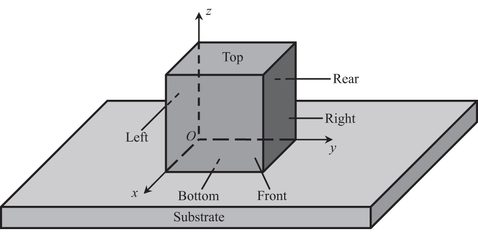
Sample on substrate.
The AM equipment and optimized manufacturing parameters are provided by SLM Solutions Group AG (Germany). Detailed manufacturing parameters are listed in Table 1. When manufacturing is completed, the samples are separated from the substrate by wire cutting. For each sample, we define the outside of the last printed layer as the top, the surface separated from the substrate as the bottom, and the remained four surfaces as the left, front, right, and rear, respectively. Post-treatments such as surface finishing and heat treatment are not applied.
Additive Manufacturing Parameters
Due to accidental failures in the manufacturing process, there are offsets along the –x direction in the Group 2 samples, as illustrated in Figure 2. The offsets in the front and rear sides of Sample 2A are denoted by Offset 1 and Offset 2, respectively. The offsets in the front and rear sides of Sample 2B are denoted by Offset 3 and Offset 4, respectively. Offsets 1 and 2 are 31 mm high from the bottom, and Offsets 3 and 4 are 23 mm high from the bottom. The offsets are measured by film thickness meter and are given in Table 2.
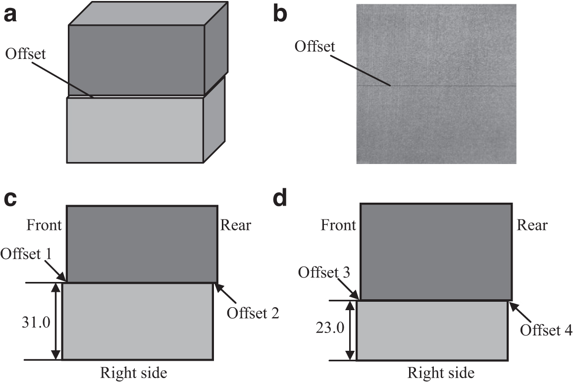
Offsets in the Group 2 samples (unit: mm).
Values of Offsets (Unit: μm)
Assessment of Quality Characteristics
AM is a process of melting metal powder or wire point by point (or line by line) and forming component layer by layer. Compared with traditionally manufactured component produced by casting and forging, AM component has sparser microstructure 41 and thereby less density. Changing AM parameters will result in different densities of manufactured component. The sparser microstructure of AM component determines that its manufacturing quality is not as good as that of traditionally manufactured component. 42 Boillat et al found that AM component has smaller conductivity than traditionally manufactured one and ascribed this property to the less density of AM component. 17 Based on the prior studies, we can conclude that conductivity is an important indicator for characterizing the printing quality of AM component. In this section, we study the characteristics of the manufacturing quality of AM component by investigating its conductivity distribution.
Conductivity measurement and results
Conductivity is measured using the eddy current (EC) method. The excitation coil with sinusoidal current generates a sinusoidal magnetic field in the surrounding space and induces ECs in the test sample. The ECs generate a secondary magnetic field, which is superposed with the primary magnetic field. The reception coil picks up the total magnetic field. The conductivity of the test sample affects the distribution of ECs, thus affecting the impedance signal of the reception coil. Establishing the relationship between impedance signal and conductivity, the conductivity can be inversed from the impedance signal.
Conductivity measurement is conducted using the EC conductivity meter FD102 produced by First Electronic Technology Co., Ltd. (Xiamen, China), as shown in Figure 3. The resolution of the conductivity meter is 0.0058 MS/m. Before measuring the conductivities of the samples, the conductivity meter has been turned on for 15 min such that the temperature drift can be ignored. The probe is placed on the top, bottom, and side surfaces of each sample, and the conductivities are read. The excitation frequency is 60 kHz and the liftoff is approximately zero throughout the experiment. An auxiliary positioning plate with 15 test positions is designed and used to make the probe positions accurate.

Measuring conductivity using EC conductivity meter. EC, eddy current.
For each position, we put the probe on the sample and read the conductivity, repeat the process twice, then takes the average value of the data as the measurement result. Tables 3 to 6 list the testing results for the surfaces of the samples, except for the front and rear sides of Sample 2A and Sample 2B due to the existence of the offsets on the sides. For the testing results on each side, the first row of the table corresponds to the initial manufacturing few layers of the sample.
Conductivities of Sample 1A (Unit: MS/m)
Conductivities of Sample 1B (Unit: MS/m)
Conductivities of Sample 2A (unit: MS/m)
Conductivities of Sample 2B (unit: MS/m)
The key factors on the obtained performances include the excitation frequency, the resolution of the conductivity meter, and the edge effect. The excitation frequencies matched with the conductivity meter are 60 and 120 kHz. To minimize the influence of surface roughness of the test sample, 60 kHz is selected. The resolution of the conductivity meter (0.0058 MS/m) is only 0.04% of the conductivity of the test sample (about 15 MS/m), which ensures high-precision measurement. To avoid the influence of edge effect, the distance between the coil and the edge of the sample is greater than 12 mm according to the manual of the conductivity meter.
Assessment and discussions of quality characteristics
For each sample, we calculate the average conductivity of the top by taking the mean of the conductivities measured at the test positions of the top. Likewise, the average conductivity of the bottom and the average conductivity of the sides of each sample are obtained. As the conductivity inside a sample cannot be measured, we use the mean of the average conductivities of all the surfaces, that is, the top, bottom, and sides, to represent the average conductivity of the sample. The results are shown in Table 7.
Average Conductivities of the Samples (Unit: MS/m)
The average conductivities of the samples are similar and less than the published conductivity of aeronautical AlSi10Mg (21.46 MS/m) 43 with reductions of about 30%, which reveals that the quality of AM samples of as-built state is worse than that of traditionally manufactured samples. This is consistent with the result reported in the study by Sharratt. 28 Furthermore, we compare the conductivities of the different surfaces for each sample and find that the average conductivity of the sides is larger than those of the top and bottom, from which we can conclude that the quality of the sides is better than those of the top and bottom.
Observing Tables 3 to 6, we also find that the conductivities at different test positions of each surface of each sample have apparent differences, indicating the nonuniformity of AM sample, which is also reported in the study by Han. 30 Besides, we compare the levels of nonuniformity of the surfaces of a sample. The standard deviations of the conductivities measured at the test positions of the top, bottom, and sides are calculated, respectively, and used to quantify the nonuniformity of the surfaces of the samples. The results are shown in Table 8. The standard deviations of the conductivities of the sides are 2.4–8.0 times larger than those of the top and bottom. That is, the levels of nonuniformity of the sides are much larger than those of the top and bottom.
Standard Deviation of Conductivities of the Samples (Unit: MS/m)
As the sides exhibit apparent nonuniform quality characteristic, we investigate the distribution of conductivity along the building direction. Figure 4 shows the average of the conductivities measured at the test positions at each height of each sample. It shows that the conductivity decreases as the built height increases. The maximal errors of the conductivities of the samples of Group 1 and Group 2 are as small as 0.05 and 0.06 MS/m, respectively, which indicates that the samples manufactured with the same process parameters have similar conductivities and the obtained conductivity distribution characteristic is reliable.

Conductivities at different built heights.
The mechanism of the conductivity distribution characteristic in the built height direction is analyzed as follows. AM uses substrate as support for layer-by-layer manufacturing. In the initial printing stage, the manufactured layers are of high quality because the heat inside the printed layers dissipates through the substrate and the stress inside the layers disperses. 44 As the manufacturing progresses, the manufacturing layer moves away from the substrate, and the influence of substrate on the dissipation of heat and dispersion of stress inside the printed layers becomes less, leading to a decrease in the quality of manufacturing layer.
Inspection of Offset
Inspection of offset based on the reference curve
A reference curve describing the quality characteristic along the building direction as expounded above is produced and offset inspection is carried out with the help of the curve. The reference curve is defined as the curve of the averaged conductivities at different heights on the sides without offsets of the samples. For the Group 2 samples, the reference curve is the average of the curves in Figure 4b, which represents the conductivity–height relation of the left and right sides that do not have offsets.
The relations of conductivity versus built height for the front and rear sides of Samples 2A and 2B are obtained following the method described in the Assessment of Quality Characteristics section and are shown in Figure 5. The reference curve is also shown in the figure for the convenience of comparison.
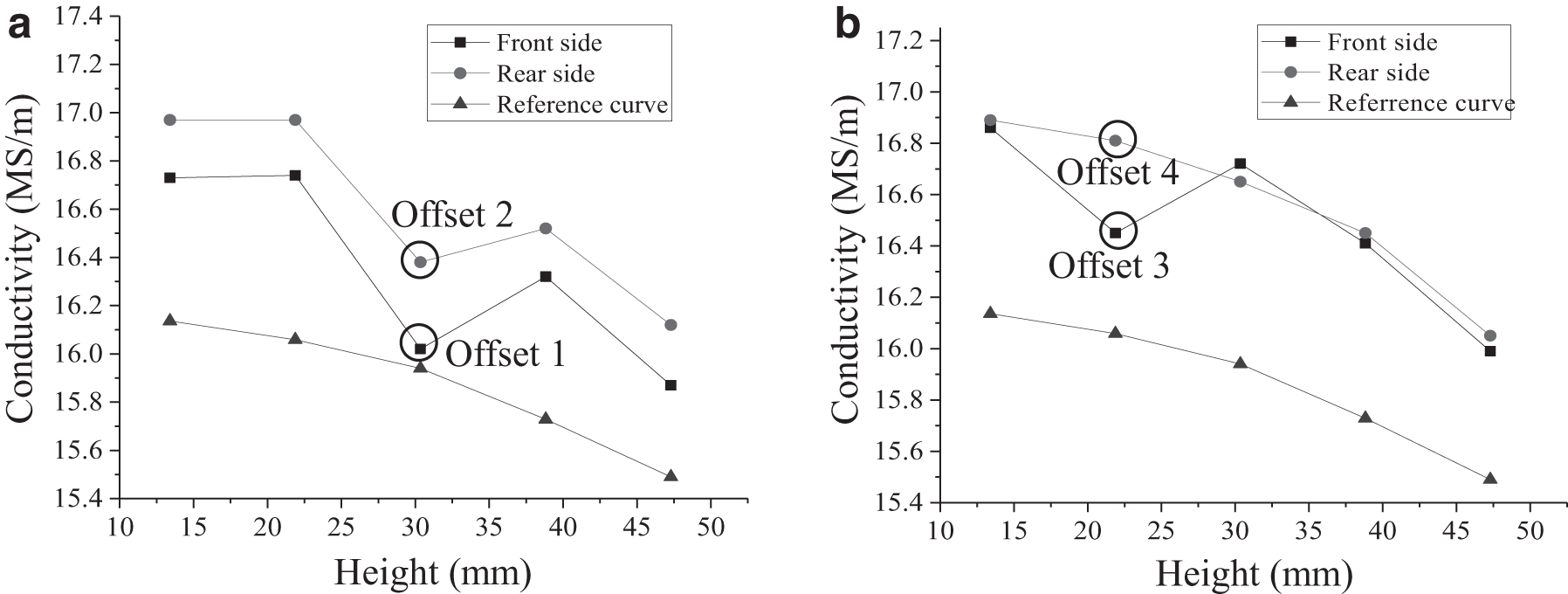
Results of offset inspection by measuring conductivity.
It is found that the conductivities of the front and rear sides are larger than the conductivities of the left and right sides. When producing the samples, the laser scans between the front and rear sides. At these two end surfaces, the time of heating by the laser beam is longer than at the other positions, to a certain extent, resulting in better manufacturing quality and greater conductivity.
Offset 1 (96 μm), Offset 2 (84 μm), and Offset 3 (37 μm) are detected as obvious troughs appear in the conductivity–height relation curves at the locations of these offsets. The curve for the rear side of Sample 2B is as smooth as the reference curve, which means that Offset 4 (13 μm) is too small to detect.
Comparative experiment and discussion
This section uses the radiography testing (RT)45,46 that is widely used in testing AM components to inspect the offsets in the Group 2 samples and compare its inspection ability with that of the method proposed in the Assessment of Quality Characteristics section. The RT is performed in Xiamen Coway Inspection Co., Ltd., by qualified operator. The sensitivity of RT is calibrated according to the characteristics of the samples. The X-ray tube voltage is 170 kV and the exposure time is 1.5 min. The X-ray is incident from the sample's top, left, and front, respectively, and the results are shown in Figure 6. The offsets are not discovered. This is because the penumbra associated with the cone beam makes the sensitivity of RT decreases significantly with increasing sample thickness. 47 The results indicate that the proposed method with the help of the reference curve is superior to the classical RT in detecting small offsets.
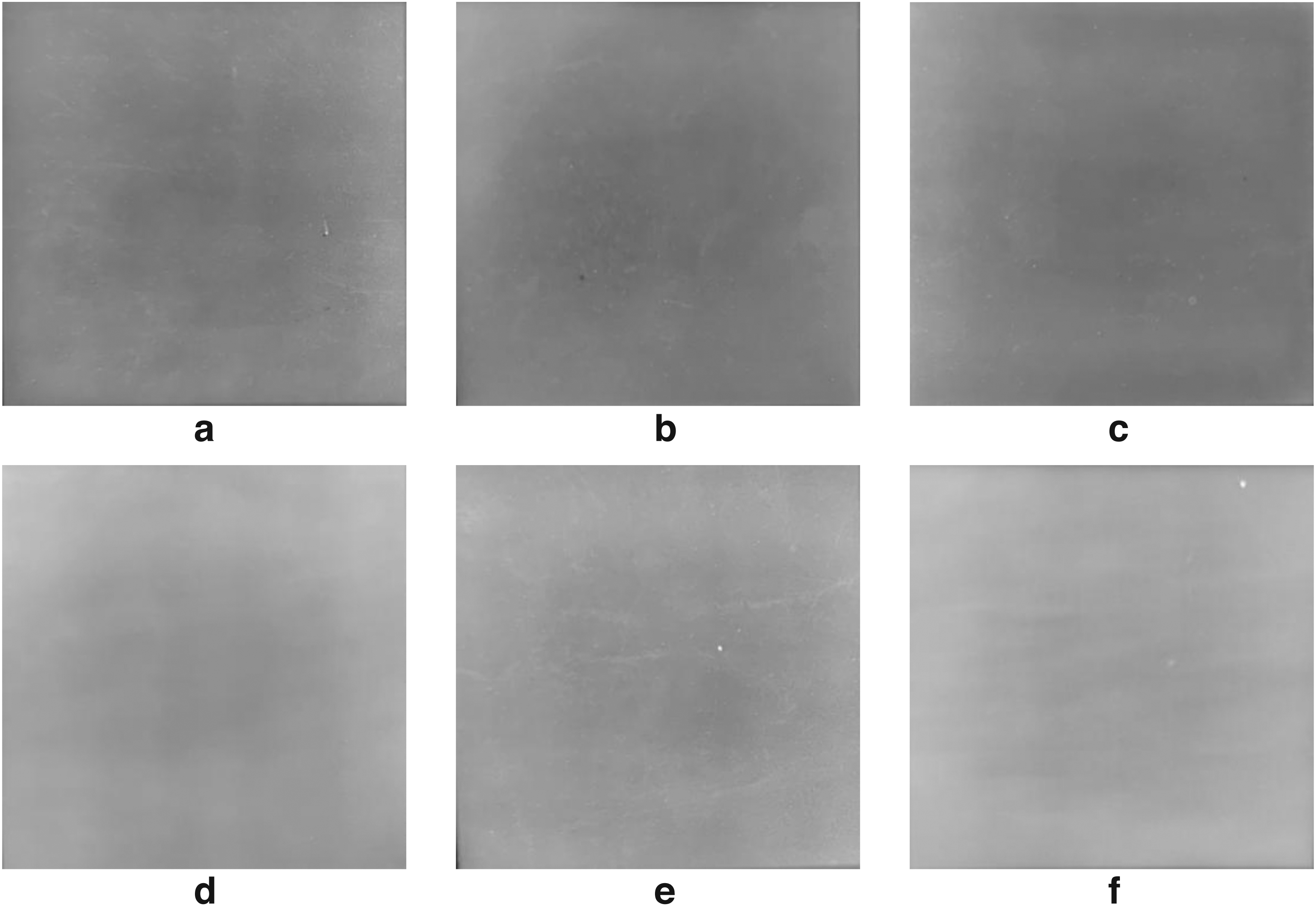
Results of offset inspection by RT.
No offset was found in the radiographic testing. Since the maximum size of the offset is 96 μm, it can be concluded that the sensitivity of the radiographic testing is bigger than 96 μm. For conductivity measurement based on the ECs method, the offsets bigger than 37 μm are discovered, but the offset of 13 μm is not discovered, which means that the sensitivity of conductivity measurement is smaller than 37 μm but bigger than 13 μm. It proves that the method of conductivity measurement has significant advantage in offset testing over the radiography.
Conclusions
AM aeronautical AlSi10Mg has broad application in the aerospace industry. The fast moving of laser beam and point-by-point melting process of AM lead to complex quality characteristics of the components, especially at their as-built state. The unclear, complex quality characteristics have been an obstacle of reliable nondestructive testing of AM components. This article investigates the conductivity characteristics of as-built AM AlSi10Mg components to reveal their quality characteristics. On this basis, the inspection of small offsets in as-built AM AlSi10Mg components is carried out.
Experimental results show that the measured conductivities are smaller than the published conductivity of aeronautical AlSi10Mg. The conductivity of as-built aeronautical AlSi10Mg is nonuniform, and the nonuniformity is much more apparent on the sides than on the top and bottom of the sample. These indicate that the AM component has less quality than the traditionally manufactured component and the quality is nonuniform. The decrease of conductivity with increasing built height implies that the quality decreases as manufacturing processes. The mechanism is related to the substrate. The use of substrate is helpful for dissipating heat and dispersing stress in the printed layers. Therefore, the initial printed layers have better quality and larger conductivity than the other printed layers.
Reference curve describing the quality characteristic in the building direction is generated. With the help of the reference curve, offset inspection is carried out and the offsets as small as 37 μm are detected. As a comparison, the offsets are also tested by the RT and no offset is discovered, revealing significant advantage in offset detection with the help of reference curve.
Footnotes
Acknowledgments
The authors sincerely thank Prof. Daoheng Sun and Mr. Kunpeng Zhang with Xiamen University for providing the film thickness meter for measuring the offsets.
Authors' Contributions
P.D.: Conceptualization, methodology, validation, formal analysis, data curation, investigation, and writing—original draft. Z.Z.: Methodology, resources, formal analysis, writing—review and editing, supervision, and project administration.
Author Disclosure Statement
No competing financial interests exist.
Funding Information
This work was supported by the National Natural Science Foundation of China under grant 52077184 and by the Natural Science Foundation of Fujian Province, China (grant no. 2019J01040). The research was supported by Xiamen Key Laboratory of Optoelectronic Transducer Technology and Fujian Key Laboratory of Universities and Colleges for Transducer Technology.