
Abstract
This article presents the design and implementation of a 3D-printed pyramidal horn antenna operating at 60 GHz, using a low-cost commercial metallic filament. The study proposes new printing parameters and a sintering process for the filament that is adapted to the requirements needed for antennas in the V-band. Surface roughness and chemical material composition were analyzed to assess the viability of usage of this filament for millimeter wave applications in terms of possible introduced losses by these parameters. Finally, three antenna samples are constructed and measured, having results with good agreements when compared with full-wave simulations, confirming the feasibility of using these low-cost filaments for candidate bands of 5G communication systems.
Introduction
The expansion of 3D printing applications within the industry is a tangible reality that we encounter daily. Various manufacturing technologies, including fused filament fabrication (FFF), stereolithography, selective laser sintering (SLS), and direct metal laser sintering (DMLS), enable the creation of numerous prototypes or components that were previously either prohibitively expensive or even unfeasible to produce.1–5 Among the potential applications, one area of interest is their utilization in high-frequency electromagnetic devices.6–12
The adoption of higher frequencies for emerging communication standards, primarily within the millimeter wave (mmWave) spectrum, introduces challenges in developing prototypes due to increased expenses and complexities. This is largely attributed to the fact that the dimensions of these prototypes are tied to the wavelength currently undergoing reduction. 9 Considering this scenario, the utilization of 3D printing technology is gaining traction, particularly in the context of cost-effective solutions.13–15
However, a notable constraint of budget-friendly 3D printing is its limited capability to produce fully metallic components. Such components are pivotal for high-frequency devices, and until recently, they were exclusively feasible through technologies such as SLS or DMLS, although at a higher cost. The introduction of metallic filaments compatible with FFF printers presents a viable solution for creating metallic prototypes while adhering to a cost-effective and straightforward approach.
Conductive filaments designed for compatibility with FFF 3D printers are readily available in the market. Some of these filaments incorporate metal or carbon additives to achieve conductivity. An example is Electrifi, 16 a filament notable for its low resistivity of 0.006 Ω/cm, rendering it suitable for high-frequency applications.17–19 Nonetheless, these filaments come with certain limitations in their applications. The conductivity reduction is contingent on the printing parameters, achievable form factor, and resulting surface roughness, making them incompatible with mmWave spectrum applications.20–23
Conversely, filaments with higher metal particle content exist, but they necessitate supplementary processes for implementation. Among these, the conductive filaments introduced by The Virtual Foundry 24 stand out. Notably, their copper-based solution contains ∼90% copper particles. However, these filaments exhibit a drawback: achieving 100% metal parts requires thermal debinding and sintering treatments in a high-temperature oven.
The aim of this treatment is to eliminate the polymer content and attain a fully metallic structure. Although this copper filament can attain properties akin to those produced by DMLS technologies, it does come with certain limitations. These include porosity, volume losses, size reduction, and nonisotropic characteristics stemming from the necessity to eliminate the polylactic acid (PLA) material. In contrast, DMLS technology excels at printing 100% metal parts with remarkable precision and layer heights of ∼20 μm, all without necessitating extensive post-processing.
Nevertheless, its widespread utilization is hindered by its elevated cost. In light of these developments, it becomes imperative to assess the potential of these novel filaments for employment in mmWave technologies. Their ability to offer a cost-effective solution for prototyping should be thoroughly evaluated.
This study proposes the implementation and evaluation of a V-band pyramidal horn antenna using the copper filament of The Virtual Foundry. 24 The novelty relies on the use of low-cost processes and off-the-shelf filaments to produce an antenna operating in the millimeter wave spectra, were parameters as surface roughness, dimensions stability and conductivity are critical. For this, a low-cost 3D printer will be developed that can use this metal-plastic filament properly to obtain high resolution, ease of printing, and the ability to manufacture complex geometries.
This includes a debinding and sintering process that will fit the requirement of the implementation for these kinds of complex topologies. For that, a parametric study that involves mass, porosity, densification, and surface roughness will be conducted. Finally, the electromagnetic properties of the 3D-printed antenna will be measured and assess its capability for implementation in the mmWave spectrum.
Methods
Design and simulation of a pyramidal horn antenna in the V-band
Horn antennas constitute a standard topology for high-gain mmWave technologies. However, their cost escalates when operating with smaller wavelengths due to the fabrication methods employed, primarily milling, and the surface treatment necessary to achieve the required surface roughness within these frequency bands. This study presents the design of a pyramidal horn antenna intended for operation within the V-band, a candidate band for 5G communication systems. The antenna covers a frequency range spanning from 50 to 75 GHz, with an operational frequency set at 60 GHz.
Figure 1 illustrates the antenna design conceived for this study, along with its associated dimensions. The design features a pyramidal horn that spans the entirety of the V-band spectrum, boasting a gain of 15 dBi at 60 GHz. The specified dimensions are as follows: a = 3.759 mm, b = 1.88 mm, A = 12.2 mm, B = 9.3 mm, DE = 9 mm, LE = 7.2 mm, and RE = 10.1 mm. It is important to note that these dimensions and the maximum achievable gain are constrained by the dimensions of the crucibles available for the subsequent sintering process.
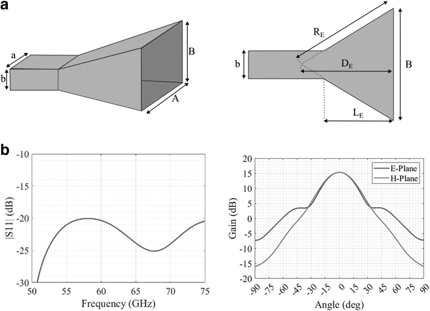
Horn antenna.
In Figure 1 are also shown the simulated results using full-wave setup for the reflection coefficient |S11| and the gain in dBi, for both planes using ANSYS HFSS. 25 For this ideal scenario we use perfect conductor for the metals, and a waveport to excite the antenna structure. We can see that the antenna is matched over the whole band of operation, while the gain reaches a value of 15.3 dBi.
Three-dimensional printing and sintering processes
To address the 3D printing process using the metal-plastic filament, we propose the use of a low-cost custom FFF 3D printer. This printer features NEMA 17 0.9° motors and a 32-bit controller board with micro-step subdivision of up to 64 times, allowing to increase the printing resolution and a direct extrusion system. The used heatbreak is bi-metal, which allows an easing melting of the materials with heat conduction up to 60% greater with respect to a single metal compound heatbreak. 26 A reinforced steel nozzle has been selected, highlighting its resistance properties to wear at its maximum operating temperature, close to 500°C, 27 and to avoid abrasion, as the filament in use has >85% copper particles. The software to be used will be the Prusa Slicer 2.3. 28
The configuration of the retraction process is a key factor as this filament has a large number of metallic particles, it becomes very brittle and, when heated, turns into a viscous mass with a texture like clay, and causes obstructions in the nozzle. To avoid that, the retraction has been set to 0 mm. In addition, 3D printing directions must be configured to avoid sudden changes in speed, acceleration, and direction, reducing the number of transfers of the nozzle in the construction process of the piece. For that, all pieces are set to be printed as only perimeters, avoiding internal filling parameters. This configuration will assure a 100% infill of the piece but avoids sudden changes in the printing direction of the nozzle due to the type of lines of the infill patterns, as shown in Figure 2a and b.
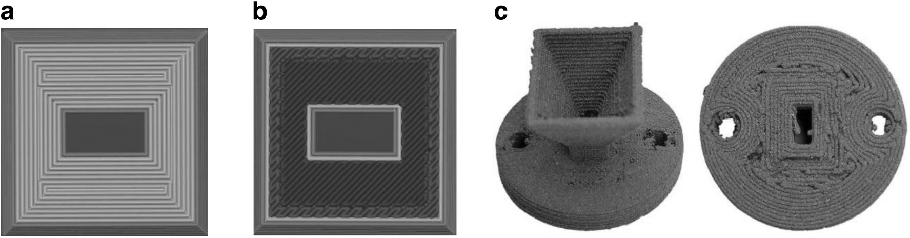
Printing directions and resulting samples.
The manufacturer recommended the use of nozzles with a diameter of at least 0.6 mm, a printing speed of 60 mm/s, a fuser temperature between 205°C and 235°C, a heating platform temperature from 40°C to 50°C, and the use of layer heights as large as possible to avoid clogging in the 3D printing process. 24 These parameters allow the 3D printing process, but they can present problems in mmWave devices with respect to the dimension stability or target surface roughness, which introduces additional losses.17–20 A first printing test was carried out using the parameters recommended by the manufacturer, using a layer height of 0.42 mm. The results were not successful; it was only possible to print the base of the antenna (between 2 and 3 mm in height).
We have modified some parameters to adapt the printing process to the horn antenna. It has been decided to change the extruder to a dual drive version, which favors the pulling process of the material, 29 and a nozzle with a diameter of 0.4 mm, in the perspective to obtain a lower layer height in the resulting printed antenna, thus reducing its surface roughness. Using these changes, it was possible to successfully print the whole antenna structure using a layer height of 0.32 mm.
As the antenna can be printed completely, we can proceed to heat treatment and sintering for the samples. Following the recommendations of the manufacturer, a programmable oven that can reach up to 1200°C is needed to set up different temperature cycles within the process. For the debinding process, we use an alumina crucible filled with alumina (Al2O3) refractory powder. The filling process consisted of a first layer of 15 mm of powder in the bottom of the crucible, then inserting the sample on top of that layer and proceeding to fill all the remaining spaces inside and around the piece. Finally, another layer of 15 mm of alumina is placed over the filled sample.
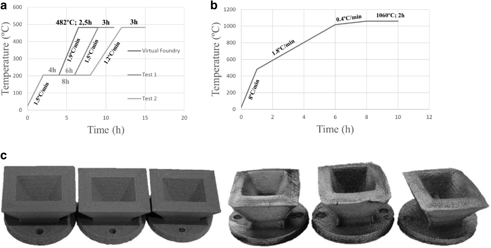
The first phase of debinding is set to eliminate all the existing plastic in the printed piece. For this cycle, the oven reaches a temperature of 482°C during a period of 9 h. At the end of the process, a layer of 25 mm of sintering carbon is applied over the refractory powder inside the crucible. The crucible is reintroduced into the furnace and the sintering process begins. In this stage, the furnace is taken up to 1060°C, while keeping this temperature for 4 h. Then, the oven is set to cool naturally, making the entire sintering process to last 2 days. For the first sintered samples, and to have symmetric pieces, which allows a better assessment of dimension reduction and possible flaws in printing, we have used standard Ka-band (only used for testing) and V-band waveguide dimensions.
The first sintering process was done using V-band standard waveguides. However, the as-is sintering process was unsatisfactory, as the samples lost their original shape, reducing their mass by 40% and their dimensions by 50% compared with the original pre-sintered sample. The second sintered samples were four slightly modified Ka-band standard waveguides, with the main modification being the addition of a 45° slope to reach the outer walls of the waveguide flange to avoid the printing of supporting structures during the process. Although these pieces kept their original shape, they experienced a loss of ∼35% of their nominal mass, and the structure was compromised with the appearance of holes, mainly in the center of the waveguide.
The sintering effects over the samples are mainly due to the low thickness of the walls of the original samples of 1 mm. Another factor that can influence the results is the layer height and temperature of the hotend. These parameters can have a direct influence on the adhesion between different layers. To improve that, we propose a reduction of the layer height and an increment of the hot-end temperature. Therefore, we performed a parametric study concerning the 3D printing and sintering results, we have found for this kind of sample, that the best results were obtained using a layer height of 0.16 mm and hot-end temperature of 220°C, while the wall thickness is set to 3.3 mm.
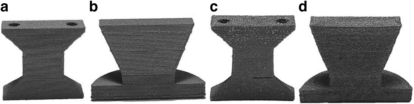
Table 1 shows the comparison between the configuration recommended by the manufacturer of the material with respect to the one obtained after the iteration process. With these new parameters, we proceed to design and print four new Ka-band waveguide samples. Each waveguide was printed scaled-up into 115% with respect to the original dimensions shown in Table 2 and design in Figure 3 (where λ corresponds to the wavelength at 28 GHz) due to an observed reduction of ∼13% on the volumetric dimensions after the sintering process.
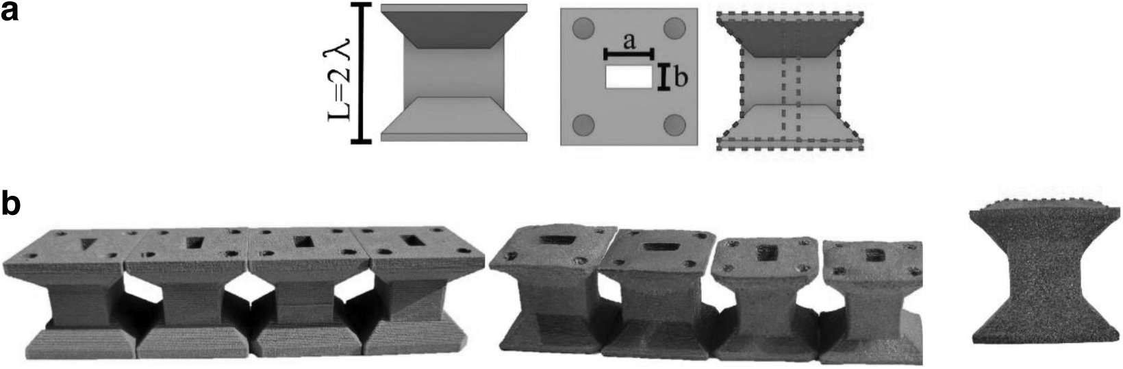
Waveguide dimensions and samples.
Printing Parameters Comparison Between the Recommendations of the Manufacturer and the Ones That Assure an Integral Sample After Sintering
Waveguide Dimensions
First, from the printed samples (Fig. 3) we can observe good homogeneity and repeatability, and a better surface finish due to the reduction of the layer height and increment of the hot-end temperature. The resulting samples after sintering are shown in Figure 3. In Table 3 are summarized the resulting mass of the printed samples pre- and post-sintering, compared with the nominal value given by the laminator software (namely reference).
Measured Mass Resulting from the Printed and Sintered Parts, Compared with the Reference Given by the Laminator Software
Another phenomenon observed post-sintering is that in all waveguides, an undulation is present on the top surface with respect to its position on the crucible. To check in which part of the process this occurred, a sample was extracted at the end of the debinding process, as shown in Figure 3. We confirmed that this effect was due to the fast slope of the temperature variation in this process, most probably due to the resulting gases trying to escape through the surface, producing this deformation. Therefore, there is a need to change the temperature rise ramp for this process.
The main changes in the process were the holding times and heating rates (Fig. 4) for the debinding process, which are dependent on the weight of the sample. In Figure 4a the blue curve shows the debinding process recommended by the manufacturer, in which the holding time was set to 4 h at 204°C, and the heating rate was 1.9°C/min between 204°C and 482°C. With this treatment, the formation of bubbles and cracks at the surfaces was important, rendering the sample useless.
Heat treatments.
To control the polymer removal and reduce the deformations of the parts during the gas formation inside the pieces structure, two test sintering processes, namely test 1 and test 2 were proposed, changing the holding time at 204°C to 6 h (orange curve) and 8 h (gray curve), and the heating rate to 1.5 and 1.2°C/min, respectively. In addition, the time at the decreasing temperature was increased to 3 h. These changes reduced part deformations before sintering drastically. Finally, the time for sintering temperature is adjusted to 2 h since, for the mass of the parts to prevent oversintering, sublimating part of the material, or more deformations.
We used this new sintering process to print and sinter three samples of a pyramidal horn antenna. Owing to the contraction of the piece and variability in copper particle percentage, we scaled the original design by factors of 113%, 114%, and 115% to achieve measurements closer to the intended design. Figure 4c displays the three scaled printed and sintered pyramidal horn antenna samples. After carrying out 60 three-dimensional printing tests, it was observed that the parts scaled at 114% and 115% obtained the closest dimensions to those proposed by design.
Statistically, and considering all the antenna dimensions, the antennas manufactured using 113% factor have an overall mean variation of a 7.98%, whereas for the samples with 114% and 115% the mean variation with the nominal values was ∼7.46%. The major variations with a higher deviation are presented in the aperture of the antenna, where the deviation in all samples goes around a 4% and 5%. In contrast, the lower variations were obtained, either in mean and deviation, for the smaller part of the antenna, which correspond to the dimensions of the waveguide that feeds the antenna and are between 1.5% and 2%.
This small variation is important for the performance of the antenna, as it is the one that will have direct contact with the transition for feeding and, therefore, any large variation of it can cause in an increment of the reflection coefficient and, therefore, a decrement on the antenna efficiency. In addition, they present a low deformation in horizontal surfaces and have no visible gaps or cracks in their structure. The resulting average dimensions of the printed samples are shown in Table 4. To notice that the reference dimensions are regarding the variables shown in Figure 1.
Average Measured Dimensions of V-Band Antennas Scaled at 114% and 115%
It is important to emphasize that the great variation in the percentage of metallic particles present in the filament causes large changes in the dimensions of the pieces when performing the sintering process, although in certain dimensions the variation is ∼1%, whereas in others it can reach up to 8%. Nevertheless, these two scaling factors will be used to print the antennas for the electromagnetic measurements.
Results
Surface roughness and composition of the 3D-printed samples
First, we proceed to measure the internal surface roughness of the printed antennas and waveguides samples, as it is important in terms of additional losses that can introduce. For this study, we print and sinter half-structures to have exposed the internal section of the samples to ease the measurement (Fig. 5).
Sample parts for surface roughness measurement.
The as-is printed samples exhibit an inner surface roughness of Ra = 6.877 μm for the waveguide sample and Ra = 9.149 μm for the pyramidal horn antenna. The larger value present on the antenna is mainly due to its internal conical geometry, whereas for the waveguide all layers are horizontal. For the sintered samples, the waveguide exhibits a surface roughness of Ra = 6.433 μm and Ra = 10.417 μm for the antenna. We can see a slight increment of the surface roughness for the antenna and a slight reduction for the waveguide. The reduced surface roughness can be explained since, in the process of removal of the polymer, the printed layers fall one on top of the other, filling the voids in between layers. Nevertheless, the obtained values are compatible with mmWave applications.20,30,31
The next studies performed were the analysis of the distribution of the particles in the printed polymer and the chemical composition of the metal-plastic filament to determine the degree of purity of the material with copper particles and to explain the sintering results. This is an important parameter, as this can have a direct influence on the electromagnetic wave propagating inside the antenna. First, two square plates of 10 × 10 × 1 mm3 are designed and printed, one kept in its original state and the other sintered.
A scanning electron microscope (SEM) over the surface is performed with a Hitachi US 3500 and EDS Quantax Esprit. In the as-is printed sample (Fig. 6a) we can see the copper particles and the PLA polymer well distributed along the surface and some voids around the larger copper particles and between the layers. For the sintered part (Fig. 6b) we can observe the metallic composition and porosity generated after the process.

In Figure 6c is shown the energy-dispersive X-ray spectroscopy (EDS) results of the measured samples. We can see that for the as-is sample, the predominant element is carbon, followed by oxygen, and finally copper. The presence of a high quantity of carbon in this sample is from the polymer composition that covers the copper particles. On the sintered part we can find mostly copper and lower concentrations of carbon and oxygen. The small presence of carbon after sintering could be due to the sample holder used.
Another interesting study is to analyze the cross-section of the printed and sintered parts. Figure 7a shows the SEM images of the fractured cross-section of both samples. From these, we can measure the size of the copper particles, which ranges from 2 to 60 μm. In addition, we can see all the voids present between larger particles and the polymer. This phenomenon was previously described in Refs.,32,33 and named “extrusion voids,” and associated with a change in the viscosity of the mixture.

On the sintered part, internal pores formed small channels between the layers inside the sample that do not reach the surface, letting the copper particles form a more homogeneous and continuous metal surface. This phenomenon was described and reported in Dizdar and Vedantha Krishna 34 on parts fabricated with bronze filaments and subsequently heat-treated to remove the polymer. This continuity on the surface is important for mmWave devices, as the propagation of the electromagnetic wave is mainly affected by surface characteristics, such as composition, continuity, and conductivity. 35
The densification of the antennas was also evaluated through the Archimedes method. An apparent densification of 70% was obtained, which is low but similar to those reported in several studies for similar materials. 32 With this test, it was also possible to determine the open and closed porosity and it is confirmed that 90% of the porosity is closed, that is to say, it is inside the piece and there is only 10% of superficial porosity. In Ebrahimi and Ju, 36 using the same Virtual Foundry material, lower densification values after sintering are obtained, and associate this result to the wide particle distribution of the filament.
Finally, in Figure 7b shows the X-ray diffractogram obtained with a Bruker D8 Advance. This test confirmed the composition of the sintered parts, having a 96.25% of copper, 1.44% of copper (I) oxide, and 2.32% of silicon oxide. The refractory powders and sintering carbon used during the thermal treatments highly prevented oxidation during the process, whereas the silicon oxide observed could be part of some additive within the filament. This low oxidation is a very important characteristic of the conductivity of the antenna and its high-frequency performances.
Millimeter wave measurements
Once confirmed that the antenna samples have surface and material properties that can be suitable for their use in mmWave topologies, we proceed to measure three printed pyramidal horn antennas. The assessment consists of the measurement of the gain radiation pattern on both planes of the antennas, to evaluate possible losses introduced by either the filament or the printing-sintering process. The chosen samples present variations of <2% in their interior measurements and up to 8% in their exterior dimensions when compared with the ideal reference case.
The setup for measurement of the gain radiation pattern is shown in Figure 8. All measurements will be performed at 60 GHz inside an anechoic chamber. Regarding the nonsintered samples, they are not suitable for mmWave applications as we need to remove the polymer from the antenna, so we can have a conductive matrix on the surface, where the surface currents can propagate. Without the sintering, this matrix is not well established, which implies extremely high losses for the antenna, or any mmWave component.
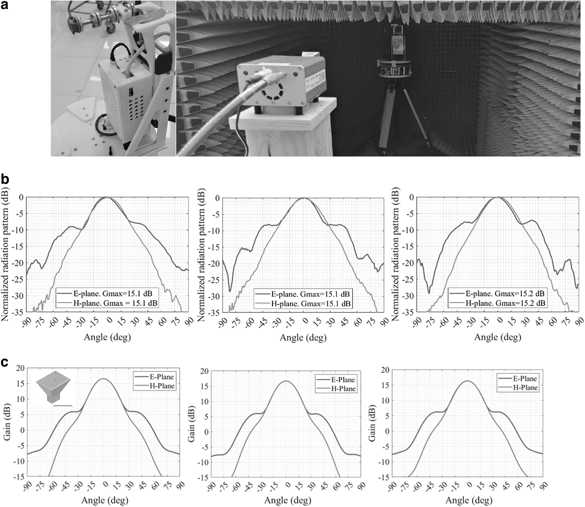
Measurement setup for gain radiation pattern measurements and measurement results.
The measurement results of the gain radiation patterns of the three sample antennas at 60 GHz are shown in Figure 8. For the three samples, a maximum gain Gmax of ∼15 dB is obtained, which is in line with the simulated results. This result demonstrates that there are no important losses introduced either by mismatching, surface roughness, or conductivity of the sintered part. In addition, we can see that for the three printed samples, measurement results are very similar on both E- and H-planes, confirming the repeatability of the printing and sintering process proposed in this study. Finally, we can see an increment in the sidelobes of the E-plane, which can be explained due to the dimension tolerance after sintering.
One last study is to see in simulation how the final dimension of the measured structures can affect on the radiation patterns in full-wave simulation. For that, we simulate the three samples that were sintered using their final dimensions and compare them with the simulated results. We can see that the results agree with the measurements, including the slight augmentations and asymmetries in the sidelobes.
Finally, when compared with other implementations in literature, 37 we can see that this proposed work can operate in a higher frequency band, where conductive and surface roughness can be an important issue, without compromising the performance of the antenna.
Conclusion
The implementation of mmWave antennas using a low-cost FFF process and sintering was demonstrated. The use of an off-the-shelf commercial filament implied a learning process of the printing and sintering process adapted for its use on a target application with strong requirements in terms of surface and composition. In addition, an optimized sintering process for the materials is proposed to achieve as close as original values of the designed ideal parts.
Composition on the sintered parts is also compatible in terms of materials and surface roughness for its use in high-frequency topologies, such as antennas, exhibiting almost the same behavior as ideal simulated counterparts using copper material. The low cost implied by the fabrication of these antennas can be a useful input for designers when implementing prototypes in these high-frequency bands.
Data Availability
The data that support the findings of this study are available from the corresponding author on reasonable request.
Footnotes
Authors' Contributions
Conceptualization, methodology, investigation, formal analysis, writing, and review by J.C. Conceptualization, methodology, investigation, formal analysis, writing, review, supervision, and funding acquisition by D.V. Data curation, measurement, visualization, formal analysis, and validation by S.B. Formal analysis, writing, review, supervision, validation, and funding acquisition by M.R. Conceptualization, methodology, investigation, formal analysis, writing, review, supervision, and funding acquisition by F.P.
Author Disclosure Statement
No competing financial interests exist.
Funding Information
This study was partially supported by ANID FONDECYT 1221090 project, ANID FOVI210008 project, DI-PUCV 37 project, and ANID FONDEQUIP EQM19002, EQM220109.