




Abstract
In this study, the effects of the surface structure of electrospun polyvinylidene fluoride (PVDF) nanoweb on surface wettability were analyzed. The conditions of the surface structure representing the lotus and petal effects were derived, and the difference in the dynamic behavior of the water droplets on the surfaces was investigated. To this end, a PVDF nanoweb was fabricated by electrospinning various concentrations of PVDF solutions. The nanoscale roughness was adjusted by varying the CF4 plasma etching time. It was seen that when the concentration of the electrospun PVDF solution was 15 or 20 wt%, a hierarchical structure of microbeads and nanofibers was formed. In the 20 wt% nanoweb, droplets formed an apparent contact angle of 149.5 ± 2.2°, and the petal effect was observed in which the droplets were pinned on the surface and did not roll off even when the nanoweb was tilted by 180°. As a result of introducing fine nanostructures with CF4 plasma etching on the 20 wt% nanoweb, the apparent contact angle increased to 162.8–164.4°, and the shedding angle decreased to 5.3–8.1°, showing a wetting transition to the lotus effect, regardless of the plasma etching time. In addition, the lotus effect was observed when 15 wt% nanoweb was treated with CF4 plasma etching for more than 10 min. We confirmed that the lotus effect was exhibited when the three-phase contact line of the PVDF nanoweb/water/air was discontinuous, and the contact area between the surface and the water droplets was reduced with increased air pockets at this interface, which led to a decrease in the adhesive force and the impact of negative pressure.
Keywords
A superhydrophobic surface is defined as the one where the contact angle of a water droplet on the surface is higher than 150° when the surface is level, and when the surface is tilted, the angle at which the droplet begins to roll off is less than 10°. 1 The self-cleaning performance exhibited by the droplet’s adsorption and removal of pollutants while rolling down the superhydrophobic surface can be reproduced by mimicking the surface of a lotus leaf; thus, the name the “lotus effect” is derived. 2 The lotus effect has drawn considerable attention and has actively been studied in various fields, from medical devices to membrane distillation.1–5 Surface wettability, which determines the practical use of a material, is affected by surface energy and surface roughness. 6 According to Young’s equation, the lower the surface energy of a solid, the higher the contact angle (θ) between the droplet and the solid surface, leading to hydrophobicity. 7 However, the maximum contact angle that can be achieved by lowering the surface energy alone, without any roughness on the surface, is limited to approximately 120°.8,9 In contrast, Cassie and Baxter 10 and Wenzel 11 theoretically demonstrated that surface roughness can maximize the surface wettability.
The petal effect is a phenomenon in which the apparent contact angle is high (152.4°) when the water droplets rest on the surface of the petal of a red rose (rosea Rehd), but they do not roll down even if the surface is completely reversed. 12 This phenomenon arises due to a hierarchical structure, having both microscale and nanoscale roughness at the same time. 12 However, as the hierarchical structure is also effective in producing the lotus effect, many studies have been conducted to identify the differences in the surface structure exhibiting the petal and lotus effects, and to reproduce these effects.13–17 For example, Huang et al. 18 compared the impact of the diameter, height, and surface structure of micropillars on the surface hydrophobicity and the work of adhesion. As a result, when the micropillar had a microlens-arrayed structure in the Wenzel state, wherein the water droplets were completely in contact with the surface, they exhibited high adhesion properties with the droplets pinned even with complete reversion. Further, the contact angle increased with a decrease in the diameter or an increase in the height of the micropillar. 18 In contrast, the micropillar with a microbowl-arrayed structure in the Cassie–Baxter state, wherein most of the interface consists of air with only a small contact area between the droplet and the surface, the droplet easily slides from the surface, exhibiting low adhesion. 18 Their study indicated that the microscale surface structure affects both surface wettability and adhesion. Bhushan and Her 19 compared superhydrophobic rose petals with different adhesion properties. They fabricated artificial hierarchical structures with different pitch and height of the microstructure and different densities of the nanostructure to explain the adhesion mechanism. Their study reported that, when the pitch and the height of the microstructure are wider and lower, respectively, and the density of the nanostructure is lower, the droplets were able to penetrate deeper into the microstructure of the surface, leading to high adhesion. 19 As can be seen from the aforementioned examples, the studies on different dynamic behaviors of the water droplets on hydrophobic surfaces have primarily focused on the comparison and analysis of surface wettability according to the size of microscale roughness, considering that the petal has a larger diameter of microstructure and a wider pitch between them as compared to those of the lotus surface.12,18–21 In contrast, a few of the previous studies have investigated the dynamic behavior of the droplets on the superhydrophobic surface by varying the nanoscale roughness and structure, which control the adhesion, and have presented the associated mechanism.22–25 However, the differences between the surface structure of a rose petal and a lotus leaf are found in the surface morphology of the nanoscale roughness structure as well as the difference in the sizes of the microstructure. Lotus leaves have nanotubules with a diameter of approximately 100–150 nm, spaced apart with a certain size of pitch. 26 However, the rose petals show continuous nanofold structures with widths of approximately 730 nm.12,27,28 In addition, there have been reports that the droplets did not roll off on the surface for a single microscale roughness structure, even with a high apparent contact angle, but rather the nanoscale surface with a single or hierarchical structure exhibited the lotus effect.26,29 These findings indicate that the nanoscale roughness has an important effect on the dynamic behavior of droplets.
In this study, nanowebs with different surface structures were fabricated by electrospinning polyvinylidene fluoride (PVDF) with low surface energy. In order to analyze the effect of the surface structure on surface wettability, we adjusted the concentration of the PVDF solution, which is one of the most influencing factors in the formation of beads, fibers, and nanowebs with various structure. 30 Plasma etching generated finer nanoscale roughness on the surface to investigate the surface structure and etching conditions for reproducing the petal and lotus effects. To this end, the first step of this study was to determine whether the lotus and petal effects were seen on an electrospun PVDF nanoweb at various concentrations with CF4 plasma etching. The second step was to analyze the surface structural characteristics that exhibited the wetting transition from the petal effect to the lotus effect. As a result, in this study, we aimed to identify the differences in the surface structure exhibiting the petal and lotus effects and to derive the surface structure conditions to obtain superhydrophobic surfaces exhibiting the lotus effect, thereby contributing to industrial applications for practical use. The surface showing the lotus effect can be used to impart self-cleaning, anti-bioadhesion, anti-bacterial/fouling, anti-corrosion, anti-fogging/frosting, and friction reduction, and the surface showing the petal effect can be applied to microfluidic manipulation and micro-templates for patterning.1,6
Experimental details
Materials
PVDF (pellet, molecular weight: ∼275,000, Sigma Aldrich, USA), N,N-dimethylformamide (Daejung Chemicals, Korea), and acetone (2-Propanone, Junsei Chemical Co., Ltd, Japan) were used. The PVDF film (thickness: 0.08 mm, Fils Co., Ltd, Japan) was cut to a size of 5 cm × 5 cm, and ultrasonification was performed using 500 mL of distilled water for 10 min; the film was then immersed in acetone for a short time for the refining process. A 10 mL syringe (Norm-ject, Germany), 22 G blunt end needle (EDGE™, China), and an aluminum foil (Hwami, Korea) were used for electrospinning. Further, a Si wafer (6-inch WAFER, LG Siltron, Korea), a 250 mesh/inch twill weave stainless steel mesh (SUS316L, Korea), and a Kapton tape (Yougwoo Fintech Co., Ltd, Korea) were used for CF4 plasma etching.
Electrospinning of polyvinylidene fluoride nanoweb
For the preparation of the PVDF solution used in electrospinning, the PVDF pellets were added at a concentration of 15/20/25/30 wt% in a 7:3 (v/v) N,N-dimethylformamide/acetone mixed solution, stirred at 100℃ for 2 h, and was then immersed in an ultrasonic bath for 30 min at 70℃. The prepared PVDF solution was loaded into a 10 mL syringe, and a 22 G needle was mounted. The solution was then electrospun onto a metal roller that was wrapped with aluminum foil, which acted as a collector. During the electrospinning process, the flow rate of the PVDF solution was 1.2 mL · h–1, the applied voltage was 18 kV, the distance between the needle and the collector was 12.5 cm, and the rotation speed of the roller was 100 rpm. 31 Electrospinning was performed in a chamber with a relative humidity of 23 ± 10% at 20 ± 2 ℃ for 3 h. The electrospun web was then dried in a vacuum oven at 70℃ for 15 h to remove the remaining organic solvent from the PVDF nanoweb.
CF4 plasma etching
In order to form fine nanostructures on the surface of the electrospun PVDF nanoweb, the samples were placed on a Si wafer, covered with a 250 mesh/inch twill weave stainless steel mesh (SUS316L), fixed with Kapton tape, and CF4 plasma etching was performed. During the plasma etching, the flow rate of CF4 gas was maintained at 20 sccm and the pressure in the chamber was maintained at 40 mTorr. The plasma etching was performed for 5/10/15/20 min by applying radio frequency (RF) power of 180 W in plasma equipment (RIE 80Plus, Oxford Instrument, UK) using the reactive ion etching method. 31
Characterization
The surface structure of the sample was observed for each condition. The chemical composition of the surface was analyzed, and the contact angle of the water droplets was measured. In the figures provided, the measurement results of the PVDF film (film) or the PVDF nanoweb are named and categorized according to the concentration of the electrospun PVDF solution (15/20/25/30 wt%) and the plasma etching time (P5/10/15/20) (e.g., 15 wt%_P20 means that the nanoweb was made using 15 wt% PVDF solution and was etched for 20 min).
Surface structure
The surface structures of the PVDF nanowebs and films were investigated at 2.0 kV acceleration voltage using field-emission scanning electronic microscopy (FE-SEM; AURIGA, Carl Zeiss, Germany). To avoid the accumulation of electron charge during the FE-SEM observation, a sputter coater (EM ACE200, Leica, Austria) was used to sputter platinum on the surface with a thickness of approximately 7 nm for 30 s at 30 mA in order to make the samples conductive.
In the SEM images, the average diameter of the nanofibers and beads constituting the PVDF nanoweb, the average diameter of the nanobuds formed after the plasma etching, and the ratio of the area occupied by the nanobuds to the total area projected from above the PVDF film were measured using Image J software (Image analyzing software; National Institute of Health, USA). The results for the three samples were averaged for each condition. In the case of the average diameter (dnano) of the PVDF nanofibers, 10 nanofibers were selected from the PVDF nanofibers that were distinct from the background on the SEM image in the order of close proximity to the surface. The diameter was measured at three points per nanofiber and the average was calculated for 30 measurement values in total. As the beads of the 15 wt% nanoweb were spherical in shape, the surface area (µm2) was obtained for 30 beads, which was measured using a two-dimensional SEM image at 10,000 × magnification; the area obtained was then substituted in the following equation, and the calculated diameter (d, µm) was averaged

In the case of the 20 wt% nanoweb, however, the beads were elliptical in shape. Therefore, the length in the direction of the fiber axis (da, µm) and the length perpendicular to the fiber axis (dv, µm) were measured for 100 beads using the SEM image at 1000 ×magnification, and each result was averaged.
After the plasma etching, for the spherical nanobuds formed on the PVDF film, the surface area (nm 2 ) of more than 40 nanobuds measured using the SEM image at 100,000 × magnification was calculated using the same method, and then the diameter (d, nm) and the ratio (%) of the area occupied by the nanobuds to the total area projected from above the PVDF film was calculated and averaged.
Surface chemical compositions
The change in the chemical composition of the PVDF nanoweb surface by plasma etching was analyzed using energy dispersive spectroscopy (EDS; XFlash® FlatQUAD 5060F, Bruker, Germany) and X-ray photoelectron spectroscopy (XPS; AXISHis, KRATOS, UK). For EDS analysis, platinum was sputtered on the surface with a sputter coater (EM ACE200, Leica, Austria) at 30 mA for 100 s in order to avoid the accumulation of electron charge.
Surface wettability
To examine the surface wettability of the PVDF nanoweb and the film, the apparent contact angles and dynamic contact angles were measured using a contact angle goniometer (Theta Lite optical tensiometer, KSV Instruments Ltd, Finland). The samples were prepared by fixing the electrospun PVDF nanoweb or film on the slide glass to measure the contact angle. Further, to measure the apparent contact angle, 3.0 ± 0.2 µL of distilled water was dropped onto the prepared sample, and the contact angle was measured after 3 s. For each sample, the values were measured at 15 different positions, and the value obtained was averaged. Repeated measurements were performed for three samples under the same conditions, and the results were averaged. In the case of the dynamic contact angle, the shedding angle, which is the minimum angle at which the droplets begin to slide for more than 2 cm, was measured when 12.5 ± 0.5. µL of distilled water was dropped from a height of 1 cm from the sample. 32 The values were measured at three different positions per sample, and the shedding angle of the three samples for each condition was repeatedly measured and averaged. While measuring the shedding angle, when the sample surface was tilted by 1° up to 90° and the droplets did not roll off the surface, the surface was turned by 180°, and the droplets were observed to verify whether they were still pinned; the surfaces on which the droplets exhibited the pinning behavior were labeled as “pinned.”
Results and discussion
Electrospun polyvinylidene fluoride nanoweb
Preliminary electrospinning with various concentrations of PVDF solutions exhibited distinct surface structures of the nanoweb, and 15, 20, 25, and 30 wt% with significant differences in the surface wettability were set as experimental concentrations.
Surface structure
The surface structure of the electrospun PVDF nanoweb was observed using FE-SEM at different concentrations, and the results are shown in Figure 1. It is observed that the nanoweb with 15 and 20 wt% concentrations of the electrospun PVDF solution has beads, whereas at higher concentrations, beads are not formed; the 25 wt% nanoweb consists of nanofibers, and for the 30 wt% nanoweb, the distinction between the fibers becomes unclear and the pores have significantly reduced.
Field-emission scanning electron microscopy images of the surface structure of electrospun polyvinylidene fluoride (PVDF) nanowebs at a magnification of 1,000 (left-hand column, scale bar: 40 µm) and 10,000 (right-hand column, scale bar: 4 µm). Each image represents the nanoweb when the concentration of the electrospun PVDF solution is (a), (b) 15 wt%, (c), (d) 20 wt%, (e), (f) 25 wt%, and (g), (h) 30 wt%.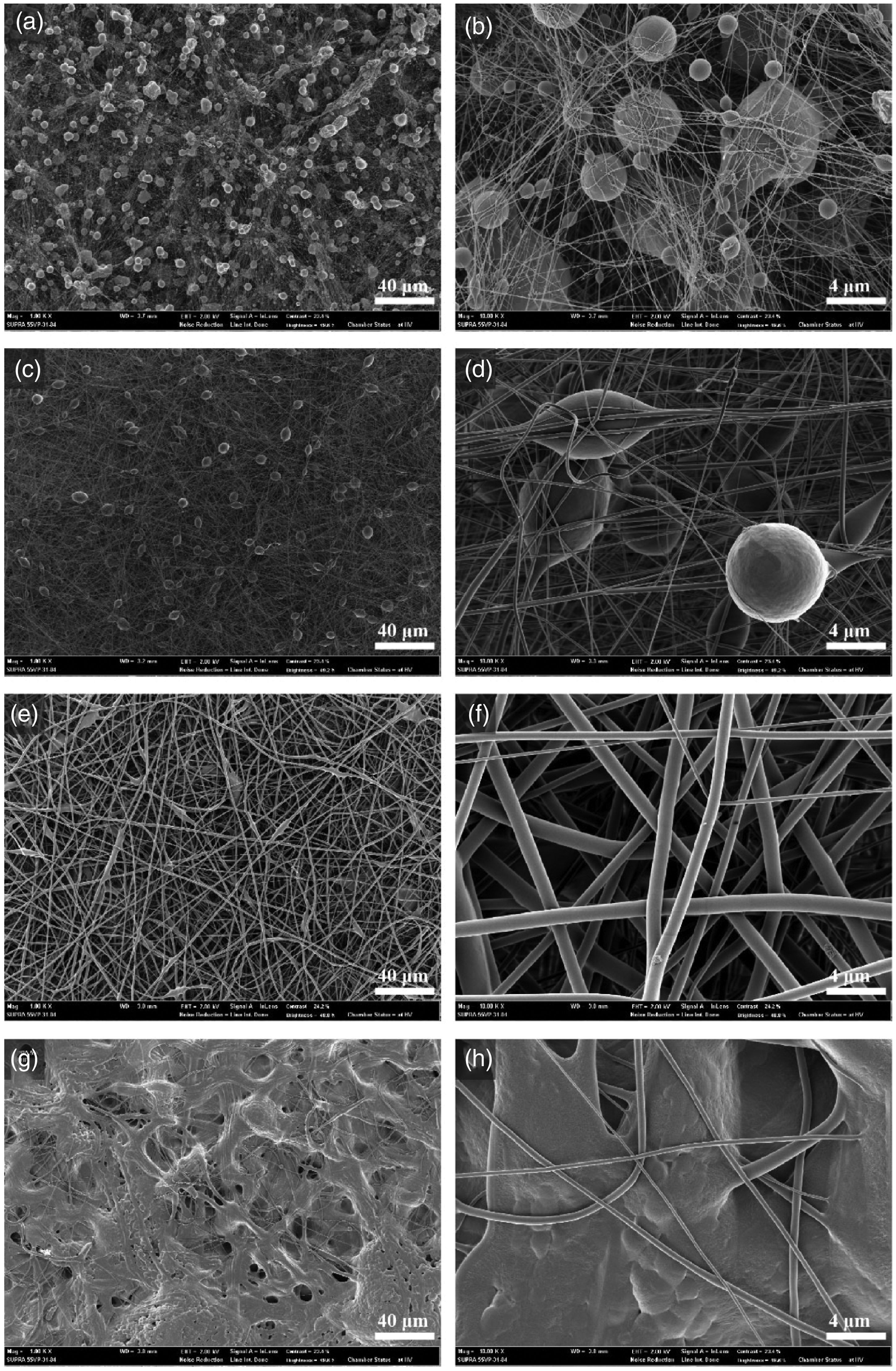
In general, the surface structure of the electrospun nanoweb is affected by the concentration, molecular weight, viscosity, surface tension, and conductivity of the polymer solution. 33 The higher the viscosity of the polymer solution, the higher the net charge density of the polymer solution jet, and the lower the surface tension, the easier it is for the electrostatic repulsion to overcome the surface tension of the solution; hence, the fibers are formed without beads. 34 In addition, the concentration of the polymer solution directly affects the viscosity of the solution, but the surface tension and conductivity of the polymer solution are influenced by the chemical composition of the solvent.30,34 Therefore, when the concentration of the polymer solution was increased to 25 wt% or more, the viscosity of the polymer solution increased; thus, the nanoweb did not form beads, but it was fiber shaped. However, at low concentrations of 15 and 20 wt%, the polymer chains in the solution were not entangled; rather, they were isolated, and the low-viscosity jets were unstable, causing the multiple-split jets to form small droplets due to the surface tension during electrospinning, which resulted in nanoweb with beads.30,35
To quantitatively analyze the roughness structure formed on the surface of the electrospun PVDF nanoweb, the average diameters of the beads and fibers were measured, as shown in Figure 2. As the concentration increased, the average diameter also increased, with beads in the range of 1.4–9.2 µm and fibers in the range of 50.5–957.8 nm. In addition, the beads exhibited a difference in shape as well as average diameter according to the concentration. The beads formed on the 15 wt% nanoweb were spherical, whereas the beads formed on the 20 wt% nanoweb had an elliptical shape with the length in the fiber axis direction (da) longer than the length in the direction perpendicular to the fiber axis (dv). As the concentration of the solution increased, the fibers became thicker, the beads became larger, and the average distance between the beads increased.33,34 Increasing the concentration of the polymer solution increased the diameter of the fibers because the cohesion between the polymers increased. This reduced the instability of whipping in the electric field, making the bending and splitting of the polymers difficult.
36
The higher the concentration of the electrospun PVDF solution, the higher the amount of polymer that solidified after the evaporation of the solvent in the spun solution; thus, it takes a relatively longer time to solidify into nanofibers. As a result, at the highest nanoweb concentration of 30 wt%, it was considered that the fibers overlapped before the solidification and the unsolidified solution flowed, which led to a significant decrease in the pores on the nanoweb (Figures 1(g) and (h)).
The average diameter of beads and fibers constituting the polyvinylidene fluoride (PVDF) nanoweb as a function of the concentration of the electrospun PVDF solution. The average diameter of beads in the axial direction (da,  ) and in the vertical direction (dv,
  ) are shown on the left Y axis, and the average diameter of fibers (dnano,
  ) of the electrospun PVDF nanoweb is shown on the right Y-axis. In the case of the 30 wt% nanoweb, the nanofibers aggregated during electrospinning; therefore, the diameter of the fiber could not be measured.
Considering all the observations, a hierarchical structure was confirmed in the 15 and 20 wt% nanowebs with microscale beads and nanoscale fiber. In particular, in the case of 20 wt% nanoweb, when its structure was compared with the hierarchical structure of a lotus leaf, in which nanotubules with diameters of approximately 100–150 nm are present on the micropapillae of diameter approximately 5–9 µm,26,37 a similar average diameter was observed in both the microstructure (da = 9.2 µm, dv = 5.1 µm) and the nanostructure (dnano = 148.3 nm).
Surface wettability
The apparent contact angles and the shedding angles of the water droplets were measured to investigate the surface wettability of the PVDF nanowebs according to the concentration of the PVDF solutions. The results are shown in Figure 3. The apparent contact angle is the highest (149.5 ± 2.2°) when the concentration of the electrospun PVDF solution is 20 wt%, followed by 15, 25, and 30 wt%. The nanowebs electrospun with 20 and 15 wt% solutions had higher apparent contact angles as compared to those of the other samples due to a significant difference in the height between the microscale beads and the nanoscale fibers, which resulted in the formation of air pockets on the nanoweb surface in contact with the droplets.10,26
The apparent contact angle ( ) and shedding angle (
 ) of the water droplets on the surface of the polyvinylidene fluoride (PVDF) film and nanowebs with different concentrations of the PVDF solution (15/20/25/30 wt%). Images of the water droplets on each surface are shown in the table, and the value of 180° (pinned) for the shedding angle denotes that the water droplet is pinned on the surface and does not roll off even when the surface is turned upside down.
In the measurement of the shedding angles, the water droplets did not roll off; however, they were pinned in all conditions until the surface was completely turned over by 180°. In particular, the 20 wt% PVDF nanoweb exhibited the petal effect in which the droplets formed a large apparent contact angle of approximately 150° and were pinned to the surface at the same time. The reason for this behavior is that the adhesive force between the nanoweb and the droplets is high, and a continuous three-phase contact line of nanoweb–water–air is formed. The electrospun nanowebs consist of numerous beads or fibers with a large surface area, so the adhesive force between the droplets and the surface of beads or fibers is high. Therefore, the droplets adhere to the surface and are pinned.
24
In addition, similar to the structure of rose petals, in which the nanofolds are present on the micropapillae,
12
the nanoweb has a structure of nanofibers laid in the direction parallel to the surface, and the droplet forms a continuous three-phase contact line along the nanofiber surface. As the water droplets are stable when the three-phase contact line is continuous, they tend to stay at the minimum local free energy. Hence, there is an energy barrier when the droplets advance or recede, resulting in strong adhesion between the surface and the droplets.25,38–40 This is because, unlike the surface of a lotus leaf, in which the nanotubes are separated from each other, the surface of a rose petal has a series of continuous nanofolds,12,27,28 and when a droplet is dropped on the surface, a continuous three-phase contact line is formed (Figure 4).
Schematic illustration of the top view (top) and side view (bottom) of the imaginary three-phase contact line formed on the surface of the lotus leaf and rose petal. The black line indicates the three-phase (water–substrate–air) contact line.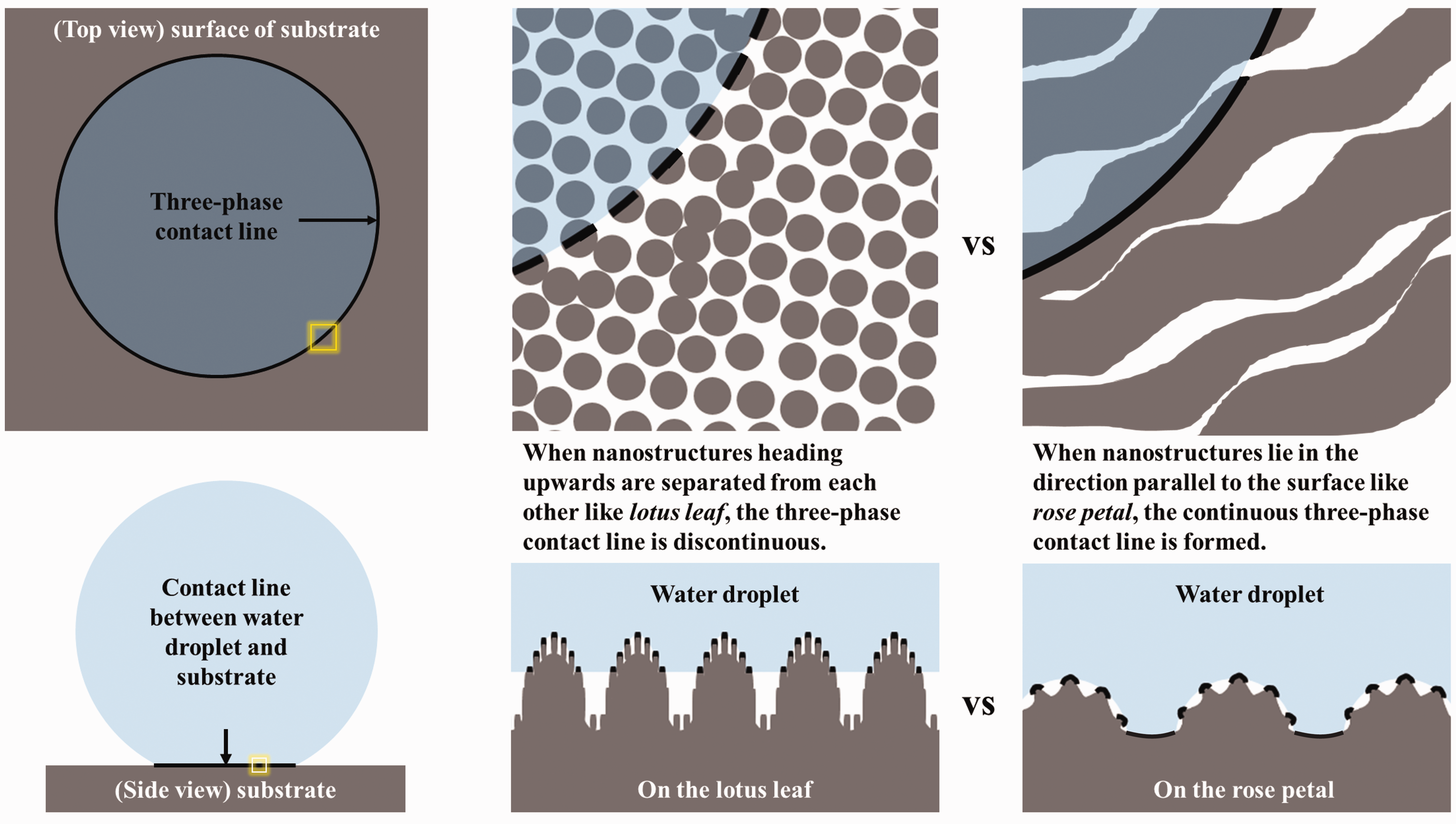
Electrospun polyvinylidene fluoride nanoweb after CF4 plasma etching
In the next step, CF4 plasma etching was used to introduce finer nanoscale roughness to the nanoweb surface to examine the effect of nanoscale roughness on the surface wettability of the nanoweb. Nanoscale roughness was varied by the CF4 plasma etching time. We investigated the conditions of the surface structure for which the change in surface wettability resulted in a transition from the petal effect to the lotus effect.
Surface structure
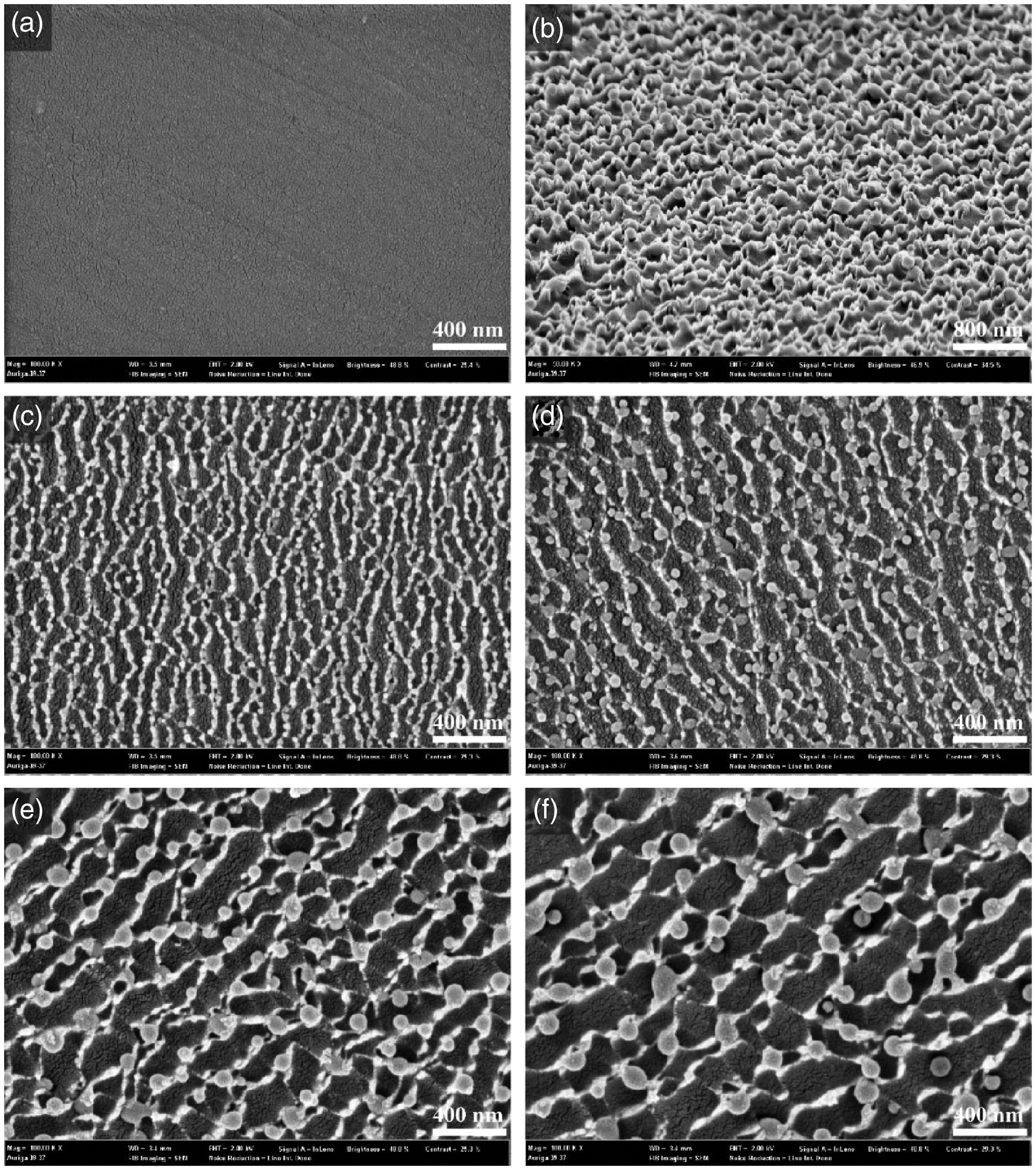
To observe the effect of plasma etching on the surface structure of the PVDF nanoweb, the surface structure was analyzed using FE-SEM, and the results are shown in Figure 5. It can be seen that fine nanoscale roughness is introduced on the surface of beads or fibers by plasma etching. For concentrations above 20 wt%, the beads or fibers on the electrospun PVDF nanoweb are maintained even after plasma etching. However, at 15 wt%, the fibers are broken and have changed into a cluster structure where several beads are aggregated. It was considered that this was because 15 wt% of the nanoweb had the smallest average diameter of fibers and beads. Hence, the nanofibers were broken owing to the plasma etching being conducted at high temperature and low pressure, and the small beads melted and aggregated with each other. Figure 6 shows the surface structure of the PVDF film after the process of plasma etching. It was observed that the longer the plasma etching time, the longer the pitch between the fine nanostructures formed in the PVDF film. The SEM image when the PVDF film was tilted at 54° showed that the film surface was etched into the shape of a concave bowl and spherical nanobuds were formed at each corner. During the CF4 plasma etching process, the stainless steel mesh as well as the sample was etched; this resulted in a reaction between the metal atoms, such as Cr and Fe, with the radicals caused by plasma, forming metal compounds.
31
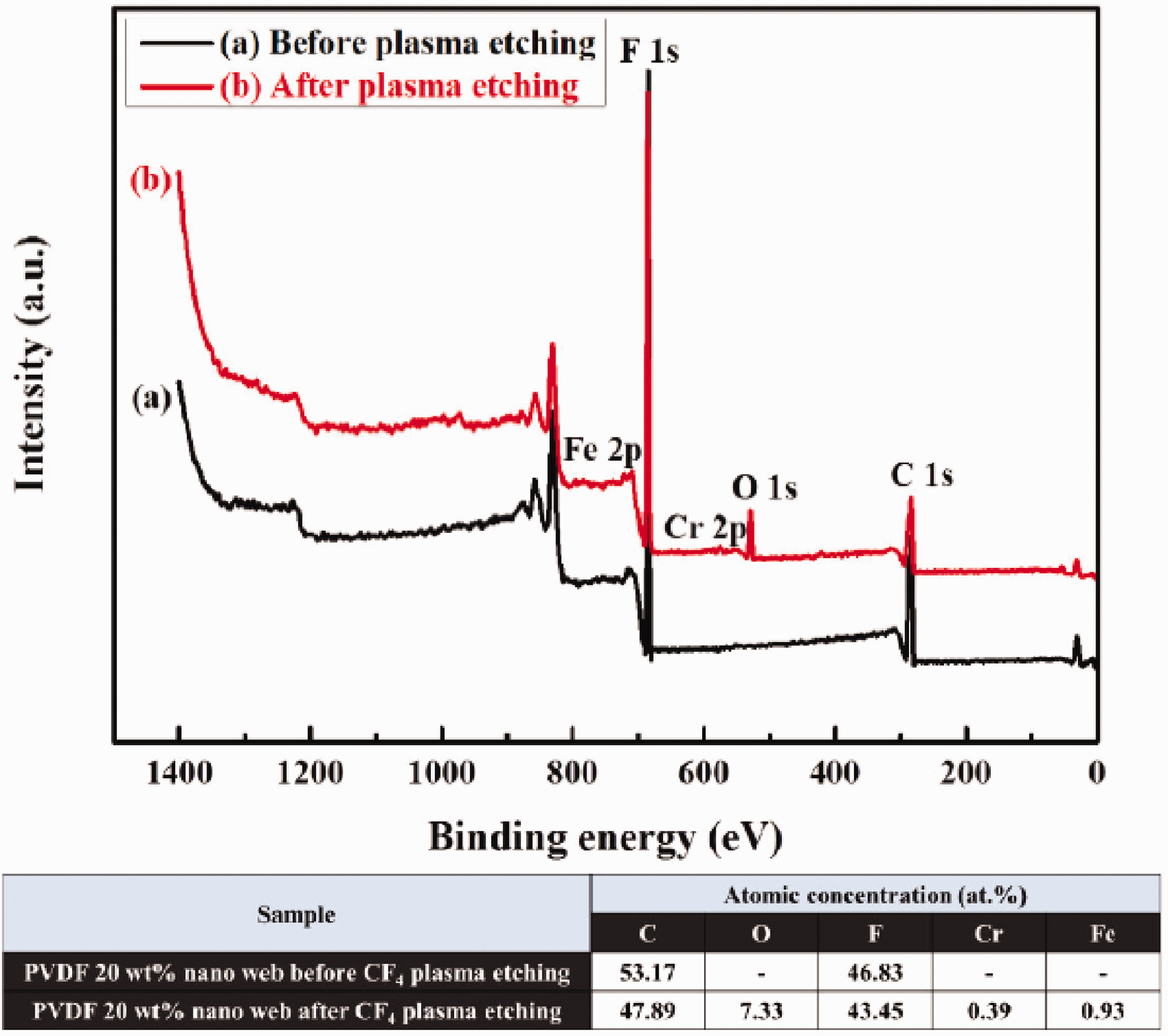
The EDS analysis of the 20 wt% nanoweb showed that Cr and Fe were not detected when the stainless steel mesh was not covered, whereas they were detected with the stainless steel mesh covered. Therefore, the longer the plasma etching time, the larger the diameter of the nanobuds because more metal ions were etched from the stainless steel mesh. However, these nanobud surfaces are considered to have been coated with fluorine through the CF4 plasma etching, as seen from the XPS analysis shown in Figure 7. As shown in the atomic concentrations (at.%) constituting the surface, the fluorine content hardly changes with the values at 46.83 and 43.45 at.% before and after the plasma etching process, respectively.
Field-emission scanning electron microscopy images of the surface structure of electrospun polyvinylidene fluoride (PVDF) nanowebs at a magnification of 10,000 ((a), scale bar: 4 µm) and 100,000 ((b), scale bar: 400 nm) as a function of plasma etching time (X-axis) and concentration of PVDF solution (Y-axis). Field-emission scanning electron microscopy images of the surface structure of polyvinylidene fluoride (PVDF) films according to the plasma etching time at a magnifications of 100,000 ((a), (c)–(f), scale bar: 400 nm) and 50,000 ((b), scale bar: 800 nm). Each image represents the top view of the PVDF film (a) without plasma etching, (b) after plasma etching for 20 min at a tilted view of 54°, and after plasma etching for (c) 5 min, (d) 10 min, (e) 15 min, and (f) 20 min. X-ray photoelectron spectroscopy (XPS) spectra of the surface of polyvinylidene fluoride (PVDF) nanoweb with 20 wt% concentration before ((a), black line) and after ((b), red line) CF4 plasma etching. The atomic concentrations (at.%) constituting the surface of the nanoweb before and after plasma etching are quantitatively analyzed based on the above XPS spectra. C: carbon; O: oxygen; F: fluorine; Cr: chrome; Fe: iron. (Color online only.)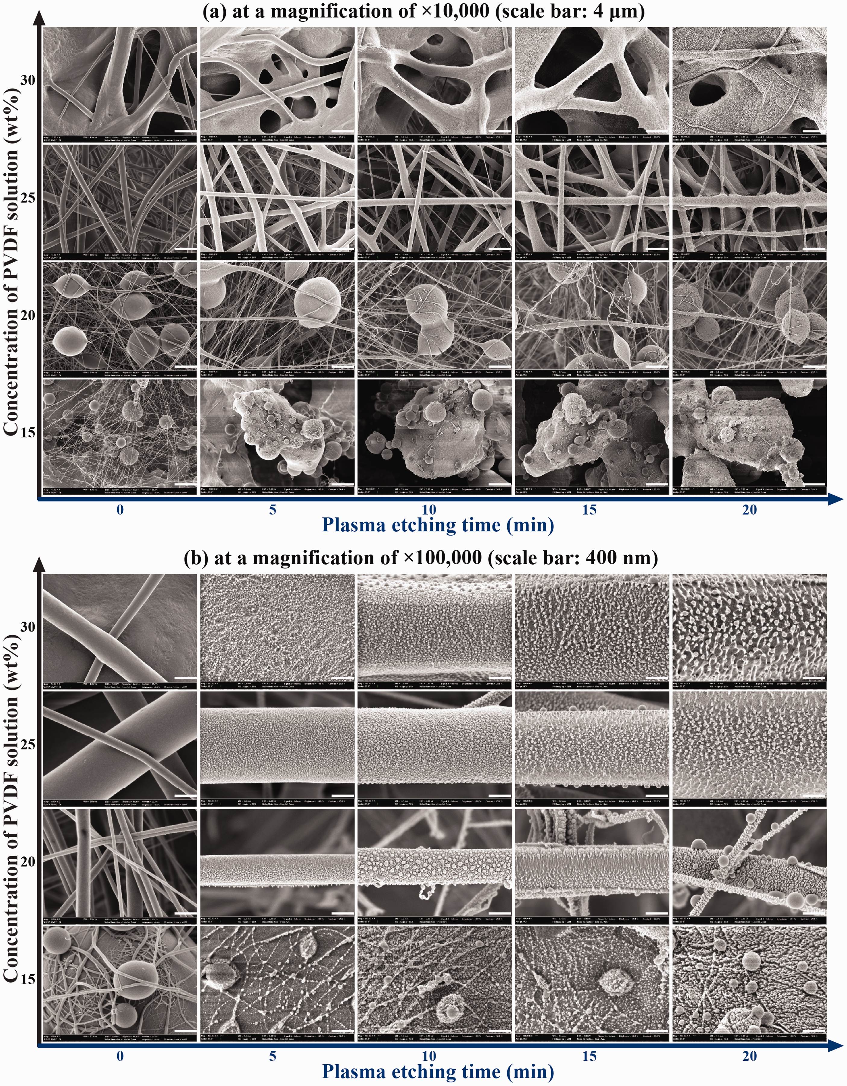
Therefore, in this study, it was considered that after the plasma etching process, only the surface roughness of the PVDF nanoweb would change and the surface energy would not change significantly. It was assumed that the bottom surface of the droplets would come into contact with the highest spherical nanobuds on the film surface. Therefore, the diameter of the spherical nanobuds formed on the PVDF film and the ratio of the area occupied by the nanobuds to the total area projected from above the PVDF film was measured. As a result, as the plasma etching time increased and the average diameter of the nanobuds and the ratio of the area occupied by the nanobuds to the total area increased, as shown in Figure 8. This tendency is also observed in the nanoweb shown in Figure 5.
Variation of the average diameter () and the average area fraction () of nanobuds on the polyvinylidene fluoride (PVDF) film as a function of the plasma etching time. The average area fraction of the nanobuds was calculated and averaged from the ratios of the area occupied by the nanobuds to the total area projected from above the PVDF film.
Surface wettability
The apparent contact angles measured to analyze the changes in the surface wettability of the PVDF nanoweb after the plasma etching are shown in Figure 9, and the shedding angle is shown in Figure 10. After the plasma etching, the apparent contact angle of the electrospun PVDF nanoweb increased and the shedding angle decreased. The nanoweb with 20 wt% concentration, which previously exhibited the petal effect, changed to exhibit the lotus effect after the plasma etching, where the apparent contact angle increased to 160° or more (162.8–164.4°). Even when the surface was slightly tilted, the water droplets rolled off easily at the shedding angles of 5.3–8.1°. In addition, the lotus effect was also observed for the plasma etched 15 wt% nanoweb. However, unlike the 20 wt% nanoweb, in which the lotus effect was exhibited after only 5 min of plasma etching, for the 15 wt% nanoweb, a stable lotus effect was observed only after plasma etching for more than 10 min. In contrast, for the 25 and 30 wt% nanowebs, although the apparent contact angle considerably increased after the plasma etching, the petal effect was still observed.
The apparent contact angle of the water droplets on the surface of the polyvinylidene fluoride (PVDF) film and nanowebs as a function of the concentration of the PVDF solution (15/20/25/30 wt%) without plasma etching ( The shedding angle of the water droplets on the surface of the polyvinylidene fluoride (PVDF) film and nanowebs as a function of the concentration of the PVDF solution (15/20/25/30 wt%) without plasma etching () and after plasma etching for 5 min ( ), 10 min (), 15 min (
 ), and 20 min (
 ). The values of the angles and images of the water droplets on each surface after plasma etching for 20 min are shown in the table, and the value of 180° for the shedding angle denotes that the water droplet is pinned on the surface and does not roll off even when the surface is turned upside down.) and after plasma etching for 5 min (), 10 min (), 15 min (), and 20 min (). In the case of the PVDF film, all values of the shedding angle are 180 ± 0° regardless of the plasma etching time, meaning that the water droplet was pinned on the surface and did not roll off even when the surface was turned upside down. As for 15 wt%_P5, 25 wt%_P5, 30 wt%_P10, 30 wt%_P15, and 30 wt%_P20, which has been indicated as the dash line, the motion in which water droplets were fixed and the motion in which they roll off at a certain angle were both observed.
To describe the change in the surface wettability of the nanoweb after plasma etching, the factors affecting adhesion between the water droplets and the surface are shown in Figure 11. After the plasma etching of the 20 wt% nanoweb, the smooth surfaces of the beads and fibers were etched and transformed into a hierarchical structure with fine nanostructures, as seen in a lotus leaf wherein numerous nanotubules are heading upward on the micropapillae.
26
Hence, when the water droplets come into contact with the nanoweb surface, the air pockets formed between the nanostructures reduce the contact area, which in turn reduces the adhesive force23,25 and breaks the continuous three-phase contact line
38
(Figure 11(a)). As a result, the adhesion between the 20 wt% nanoweb and the droplets was reduced, and a wetting transition occurred from the petal effect to the lotus effect.
Schematic illustration of the factors affecting adhesion between the water droplet and the surface: (a) formation of air pockets after introducing nanostructures by CF4 plasma etching; (b) generation of negative pressure (ΔP) according to the increase in volume of the sealed air; (c) a decrease in negative pressure (ΔP) due to an increase in the initial volume of sealed air (V0, white) between the nanostructures (gray) under the water droplet (blue) in proportion to the plasma etching time. (Color online only.)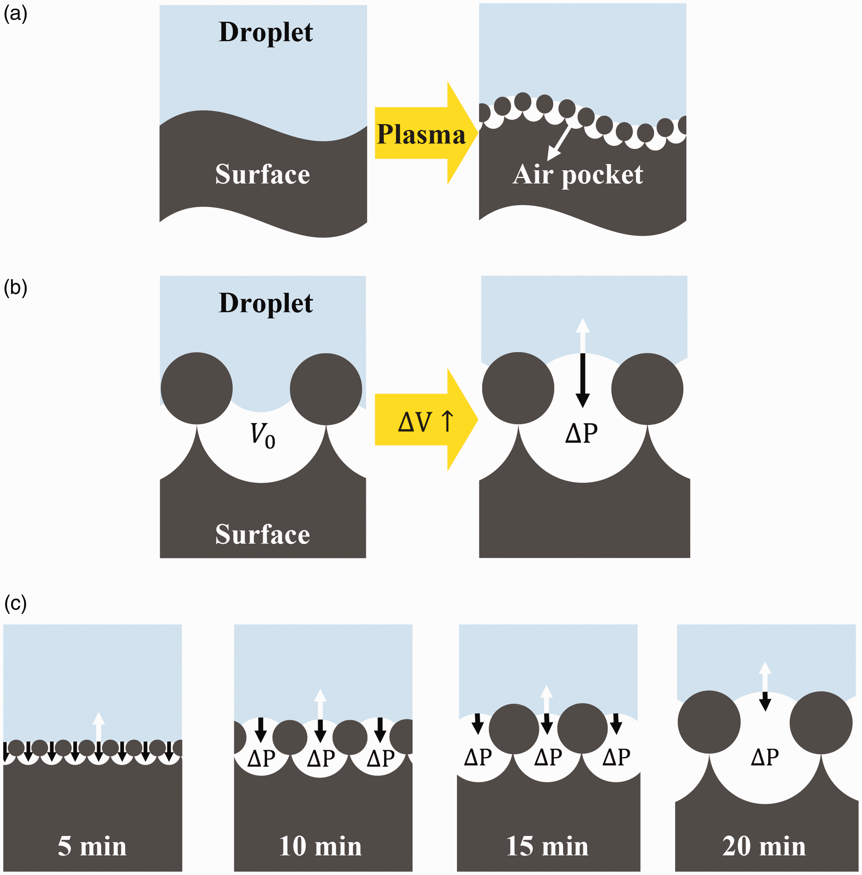
In addition, after the plasma etching of the 15 wt% nanoweb, the fibers were broken and the beads were bonded together, increasing the diameter of the microstructure with increased spacing. Thus, for the 15 wt% nanoweb, the droplets could easily penetrate between the microstructures containing relatively fewer air pockets, which increased the contact area between the droplets and the nanoweb. Therefore, this resulted in a longer plasma etching time to generate the lotus effect on the 15 wt% nanoweb with relatively high adhesion properties.
In contrast, for nanowebs with all concentrations except 20 wt%, the droplets were pinned on the surface even after plasma etching. This was because for the nanowebs having a large contact area with the droplets, the action of negative pressure had a significant impact on the adhesion.14,21,25,41,42 When the plasma etched nanoweb and the droplet came into contact, the air pocket between the fibers or beads of the nanoweb was in the open-air state through which air could freely pass through the pores. Nonetheless, the air pockets between the nanostructures that were sealed by the above water droplets did not allow air to pass through; hence, the pockets were in a closed air state. 42 In this case, when the surface was tilted or reversed to move the droplets, the droplets tried to slide away from the surface, which led to the formation of a convex meniscus at the liquid–air interface and increased the sealed air volume (Figure 11(b)).25,41 According to Boyle's law, 43 when the sealed air volume increases, a negative pressure is generated, resulting in adhesion between the water droplets and the surface.25,41
The influence of negative pressure can also be confirmed by the decrease in the shedding angle as the plasma etching time increased. The negative pressure (ΔP) is proportional to the air-expansion ratio (ΔV/V0), which is the ratio of the increased volume of sealed air (ΔV) between the nanostructures to the initial volume of the sealed air (V0). When ΔV ≪ V0, ΔP is small, and when ΔV ≈ V0, ΔP is very high.14,25,41 Thus, the longer the plasma etching time, the longer the pitch between the nanostructures and the surface is etched deeper. Hence, the initial volume of the sealed air (V0) between the nanostructures increases, and the associated negative pressure (ΔP) is small, resulting in relatively low adhesion (Figure 11(c)). 25
Surface structure for generating petal and lotus effects
Based on the aforementioned results, the proposed conditions of the surface structure for generating the petal and lotus effects are shown in Figure 12. For a surface with a hierarchical structure, four cases are possible when each surface is hydrophobic with an identical surface energy. Microstructure 1 has a larger contact area with the water droplets than microstructure 2, which has open-air pockets on the interface in contact with the droplet, and nanostructure 1 has less space between structures, which may lead to the formation of smaller initial volumes of sealed air pockets than nanostructure 2.
Schematic illustration of the proposed surface structure conditions for generating the petal and lotus effects: (a) side view of the water droplets on the flat surface and microstructures 1 and 2, where each surface is hydrophobic with identical surface energy; (b) the contact area with the water droplet (blue) of microstructure 1 is larger than that of microstructure 2, which has open-air pockets (white) at the interface; (c) when nanostructures contain a small initial volume of sealed air (yellow) between nanostructures under the water droplet, the petal effect can be exhibited in combination with microstructure 1; (d) when nanostructures contain a large initial volume of sealed air between nanostructures under the water droplet, it is advantageous to exhibit the lotus effect in combination with microstructure 2. (Color online only.)
Firstly, a single nanoscale roughness structure has a different dynamic behavior of the water droplets from the petal effect to the lotus effect depending on the volume and density of spaces between the nanostructures.22–24 As for nanostructure 1, with less space between the structures and dense formation of a small initial volume of sealed air pockets, the structure has a large negative pressure, which can exhibit the petal effect with high adhesion between the droplet and the surface.23,25 In contrast, for nanostructure 2, the impact of the negative pressure is small with a relatively large initial volume of sealed air, and has a small contact area with the droplets. Its three-phase contact line is discontinuous, showing low adhesion properties. 22
Next, in the hierarchical structure, depending on the microstructure, the petal effect can be exhibited with microstructure 1 having a larger contact area with the droplets, and the lotus effect can be exhibited with microstructure 2 having a smaller contact area with the droplets. In the petal effect, as the structure is in a Cassie impregnating wetting state, the droplets on the surface penetrate through the microstructures but cannot penetrate through the nanostructures.12,19,37 Thus, in a hierarchical structure 1-1, in which the adhesion between the droplet and the surface is strong, having microstructures with a large contact area with the droplets, and a strong negative pressure owing to the small initial volume of sealed air between the nanostructures, the petal effect with high adhesion properties can be exhibited.
In contrast, in the hierarchical structure containing the open-air pocket between the droplet and microstructure 2, its three-phase contact line is more discontinuous due to more air pockets as compared to a single roughness structure.26,38 At the same time, as the contact area is small, the adhesive force between the droplet and the surface is small, and the negative pressure is small with a low density of sealed air formed between the nanostructures. 25 Therefore, in hierarchical structures, especially in hierarchical structure 2-2, the adhesion is low and it is more advantageous to exhibit the lotus effect. 26
Conclusion
The purpose of this study was to analyze the effect of the surface structure of PVDF nanoweb on the surface wettability by varying the surface structure through electrospinning and to transform from the petal effect to the lotus effect by introducing fine nanoscale roughness with CF4 plasma etching. As a result, the petal effect was generated in the electrospun PVDF nanoweb of a 20 wt% concentration with a hierarchical structure. Further, with plasma etching for over 5 min, the surface of the 20 wt% nanoweb was etched, introducing nanoscale roughness. In this case, the petal effect was transformed into the lotus effect, in which the droplets easily rolled over with a small tilting of 5.3–8.1°. Thus, it was confirmed that when the three-phase contact line formed by the droplet on the surface became discontinuous and the contact area between the surface and the droplet was reduced, containing large amounts of air pockets at the interface in contact with the droplets, there was a decrease in the adhesive force and the impact of negative pressure, which facilitated the lotus effect. In addition, we propose further studies that can expand the boundary conditions of the lotus effect for various materials with different surface energies. Furthermore, the conditions of the surface structure for the lotus effect derived in this study can contribute to the design of practical processing that can be used to fabricate superhydrophobic surfaces. The electrospun PVDF nanoweb developed in this study exhibiting the lotus effect is expected to be applied as a smart material with a self-cleaning function.
Footnotes
Declaration of conflicting interests
The authors declared no potential conflicts of interest with respect to the research, authorship, and/or publication of this article.
Funding
The authors disclosed receipt of the following financial support for the research, authorship, and/or publication of this article: This work was supported by the National Research Foundation of Korea (NRF) via a grant funded by the Korea government (Ministry of Science and ICT; grant numbers NRF-2016M3A7B4910940 and NRF-2018R1A2B6003526) and by the Basic Science Research Program through the National Research Foundation of Korea (NRF) funded by the Ministry of Education (Grant No. NRF-2019R1A6A3A13095712).
