



Abstract
In a two-dimensional photonic crystal T-shaped waveguide with a passive switching function, the routing characteristics depending on the input light amplitude and the wavelength are numerically demonstrated by using the frequency-dependent finite-difference time domain method. For typical input electric field amplitudes (E0 = 0.1, 0.5, 1.0, and 1.5 [V/m]), the distribution ratio to the outputs is evaluated from the electric field profile. Additionally, the cross-correlation coefficient and normalized power spectra are considered. For the add/drop circuit in wavelength division multiplexing (WDM) optical network, it has been determined that the add/drop signal wavelength can be tuned by engineering the duplexer at the branching point with specific pillar radii.
Introduction
In recent years, internet traffic has surged due to advancements in optical fiber and wireless communication technologies. This increase has led to greater information processing demands on electronic integrated circuits (ICs), resulting in issues like higher power consumption and heat generation. Optical technology offers a potential solution to these problems. Consequently, various research institutions have been investigating optical ICs.1–3
Photonic crystals have garnered attention for their potential in realizing optical ICs. These artificial structures can block light within specific wavelength ranges, depending on factors such as the medium constants, lattice period, and diameter of pillar. This blocked wavelength range is known as the photonic band gap (PBG).4,5
In this paper, supposing silicon (Si) and fused silica glass (SiO2), we installed a resonator made of linear, dispersive, and nonlinear dielectric medium at the branch point of a two-dimensional photonic crystal waveguide. The resonator is expected to perform as a duplexer. The author's previous studies have confirmed optical switching using this structure.6,7 This paper examines the distribution characteristics based on changes in electric field amplitude and wavelength of the input optical signal, using a frequency-dependent finite-difference time domain (FDTD) method. This method calculates the electromagnetic field time evolution by finite-difference technique 8 and is applicable to both linear dispersive and nonlinear dielectric materials based on Z-transformation, which is known in digital filter theory.9–11 Finally, it is numerically demonstrated that tuning the add/drop signal wavelength is possible by designing diameter of silica pillars of a duplexer at the branching point. This enables to configure all-optical signal add/drop circuit by cascading proposed structures with different duplexer radius for wavelength division multiplexing (WDM) telecommunication system.
The contributions of this research are as follows: It is based on a photonic crystal structure suitable for photonic ICs. The material used is quartz glass, which is also used in optical fibers and is considered to have high compatibility with future photonic networks. Additionally, it involves the design of a passive optical packet routing circuit and the verification of its performance through simulations.
The structure of this paper is as follows. Section 2 discusses related research, particularly focusing on studies of active and passive optical packet routing, and examines the challenges for realizing future photonic networks. Section 3 briefly introduces the frequency-dependent FDTD method used for simulations. Section 4 describes the structure of the proposed T-shaped waveguide and the numerical settings for the simulations, including parameters assuming quartz glass. Section 5 presents the simulation results, showing how the output of the T-shaped waveguide changes with the input signal wavelength and confirming the effects of nonlinear optical phenomena influenced by the input signal amplitude. Furthermore, it was found that by changing the pillar diameter at the branching point of the T-shaped waveguide, specific wavelength components could be extracted at the output port. Section 6 summarizes the obtained results and mentions that the proposed structure can be applied to future all-photonic networks.
Related works
As research on active optical packet routing, the following papers can be cited. In Carena et al., 12 optical packet experimental routing architecture (OPERA) with label-swapping capability is described. The OPERA network is based on the design of optical network interface routers and supports optical Internet Protocol-related functions. The technical features are subcarrier multiplexed header addressing, packet-rate wavelength conversion, and arrayed waveguide grating router technology to achieve multi-hop routing. It is suitable for network environments requiring high-speed data transmission and low-latency communication. In Reis et al., 13 experimental implementation of an all-optical packet routing scheme using a semiconductor optical amplifier (SOA)-based Mach--Zehnder interferometer (SOA-MZI) structure is discussed. It has contention resolution capabilities and evaluates the routing function and state performance through measurements of crosstalk and bit error rate. Applications for large-scale networks and data centers requiring high throughput are considered. In Ben Yoo, 14 optical burst switching (OBS) and optical packet switching (OPS) technologies for the future photonic Internet are reviewed. Optical label switching (OLS) routers to enable the transfer of asynchronously arriving variable-length packets, bursts, and circuits is its technical advantage. It is suitable for high-performance networking supporting multimedia and data communication applications. These papers each provide significant contributions to the field of optical packet routing, focusing on different approaches and technical features. They address specific application areas and technical challenges, advancing the development of optical communication technologies. However, these systems require complex control for active signal processing.
The following papers highlight the use of passive components in optical packet routing based on conventional waveguiding structures, offering insights into their design and implementation. In Manukonda, 15 the method of achieving multi-hop gigabit Ethernet routing in a gigabit passive optical system using a genetic algorithm is explored. It is based on the design and analysis of optical fiber communication systems and achieves reliable digital data transfer using passive components. Wincy Jenefer and Karpagarajesh 16 provide an overview of gigabit passive optical networks (GPON) and describe the technology that uses passive splitters to deliver high-bandwidth voice, data, and video services. Kaur and Bansal 17 review the current trends and prospects of passive optical networks (PON) that use passive components to achieve high bit rates and long-distance transmission. These passive systems utilize conventional waveguide structures that leverage total internal reflection caused by differences in refractive index, and they are not applicable for the realization of future photonic ICs.
Papers have been published on the fabrication and measurement of photonic crystal waveguides based on Si photonic crystal structures.18,19 Additionally, lasers as signal sources can also be fabricated based on photonic crystal structures.20,21 It has been reported that photonic crystal structures are ideal for increasing the density of photonic ICs. 22 If the output from the proposed circuit is attenuated, it is possible to compensate for the attenuation by connecting an erbium-doped fiber amplifier (EDFA), a Raman amplifier (RA), or an SOA in the subsequent stage to maintain the optical signal level. By connecting the output to a fiber cable with connectors, it is easy to realize an all-optical packet routing device. Based on these findings, it is concluded that the fabrication of devices based on this simulation is feasible, and the performance confirmed by the simulation can be expected to be achieved.
Frequency-dependent FDTD method
In our previous works,6,7 we utilized a two-dimensional discretized form of Maxwell's equations for the transverse electric polarization with (Hx, Ey, Hz) components, which propagates along the x and z axes (i.e., ∂/∂y = 0). As discussed in the following section, supposing fused SiO2, we considered a dispersive dielectric medium with frequency-dependent permittivity and a nonlinear Kerr-type material, where the refractive index changes proportionally to the electric field intensity (|E|2). The Maxwell equations were formulated to incorporate this dispersion and nonlinearity of the material using a frequency-dependent FDTD method.9–11 For detailed formulation, please refer to the study of Higashinaka and Maeda.6,7
Settings for simulation
The propagation of optical signals in photonic crystal waveguide, which is composed of two-dimensional periodic array of dielectric pillars, incorporating a three-port duplexer, is analyzed. To capture optical signals leaking into the photonic crystal, an additional output port is integrated within the structure. Figure 1 depicts the waveguide structure utilized in this simulation. In this figure, the background is air. The black circles are assumed to be Si rods with linear dielectric property with index of refraction n1 = 3.6, as referenced in Sullivan. 9 The green disks are SiO2 rods with n2 = 1.5, which shows both dispersive linear and nonlinear dielectric characteristics simultaneously. The other parameters and those values are listed in Table 1 as referenced in Sullivan. 9
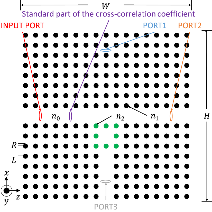
Illustration of two-dimensional photonic crystal waveguide. A duplexer is placed at T-shaped branch with 8 disks, which are composed of dielectric medium with linear dispersion and nonlinearity (indicated by green circles online).
Physical parameters appeared in the simulation. 9

The periodicity of Si and SiO2 rods is L = 551.8 [nm], with radius of the rods R = 0.2 L is used. Spatial grids for FDTD method are Δx = Δz = 9.85 [nm] and the temporal step Δt = 0.0209 [fs]. The sizes of these spatial and temporal increments were determined after confirming that the calculation results converged as the increments were refined. The analysis area spans 9.69 [µm] square along the propagation axis x and the transverse axis z. The range in which the wavelength varies is (λ = 1.350 − 1.600) [µm]. To eliminate unphysical reflection from radiative field toward outside of the analysis region, Berenger's perfectly matched layer 23 is set on the outer perimeter surrounding the analysis area.
For the settings above, a line of defect in the periodicity performs as a waveguide. The reason is that the photonic bandgap properties exhibited by the periodic structure prevent the electromagnetic field in the varied range of wavelength from penetrating into the periodic structure.
Entering Gaussian beam to port 1, which is given by

In Figure 1, three ports are illustrated for evaluation of optical field. The power 
Cross-correlation 
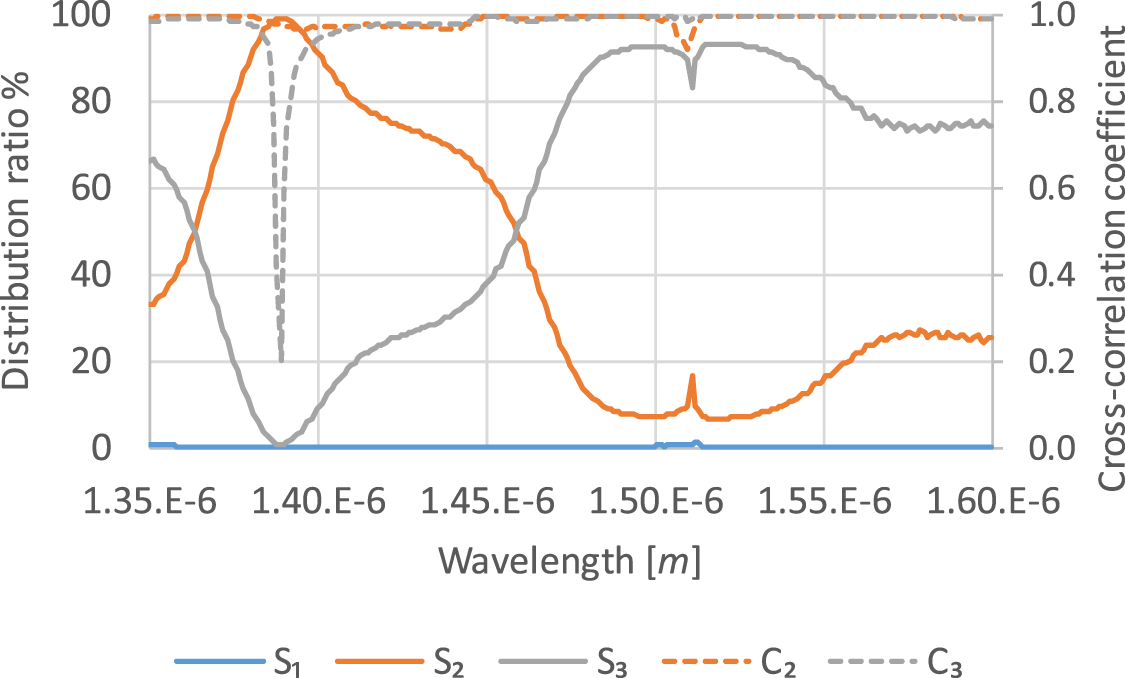
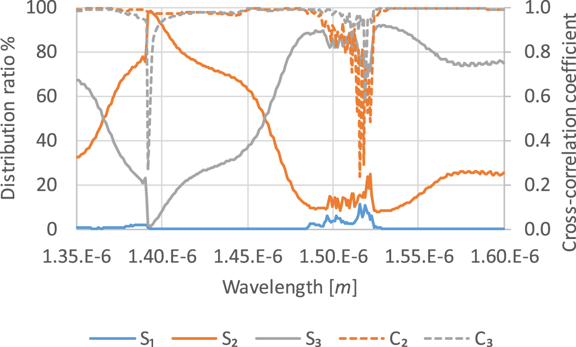
The input electric field amplitude E0 was adjusted to 0.1, 0.5, 1.0, and 1.5 [V/m] as typical examples. Figure 2 shows the distribution ratios for ports 1, 2, and 3, as well as the cross-correlation coefficient between ports 2 and 3 for E0 = 0.1 [V/m]. It was observed that the distribution ratios for ports 2 and 3 change with the input signal wavelength. The optical signal does not reach port 1, which is situated intentionally in the middle of periodicity to detect the radiation field. It is obvious that radiation could not be detected at any wavelength due to photonic bandgap caused by periodic array of linear dielectric pillars. It is evident that the proposed periodic structure works as a photonic crystal for the operating band of wavelength.

The distribution ratios of ports 1, 2, and 3, along with the cross-correlation coefficient between ports 2 and 3 for
Additionally, the cross-correlation value exceeds 0.9 in wide range of the wavelength, indicating a high similarity of electric field profile between the reference part (port 1) and the modes of each port (ports 2 and 3). However, at λ = 1.388 [µm], the cross-correlation for port 3 is quite low, indicating no correlation between the profiles of the reference part and of port 3.
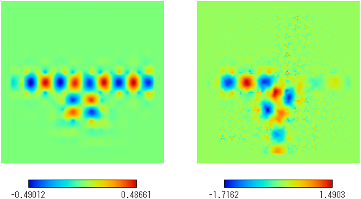
Figure 3 shows the electric field distribution at wavelengths λ = 1.388 [µm] (left) and λ = 1.516 [µm] (right), respectively. It is evident from Figure 3 that the signal wave does not get to port 3 at λ = 1.388 [µm].

Electric field distribution for
Figure 4 presents the distribution ratios for ports 1, 2, and 3, as well as the cross-correlation coefficient between ports 2 and 3 for E0 = 0.5 [V/m]. The results indicate that the distribution ratios and cross-correlation coefficients are similar to those observed for E0 = 0.1 [V/m]. However, around λ = 1.500 [µm], minor variations in the distribution ratio and cross-correlation coefficient should be noted.
Distribution ratio of port 1, port 2, and port 3 and cross-correlation coefficient of port 2 and port 3 for
Figure 5 illustrates the electric field profiles at λ = 1.388 [µm] (left) and λ = 1.516 [µm] (right), respectively, confirming that the optical field is radiated into the periodic structure at λ = 1.516 [µm].
Electric field profile for
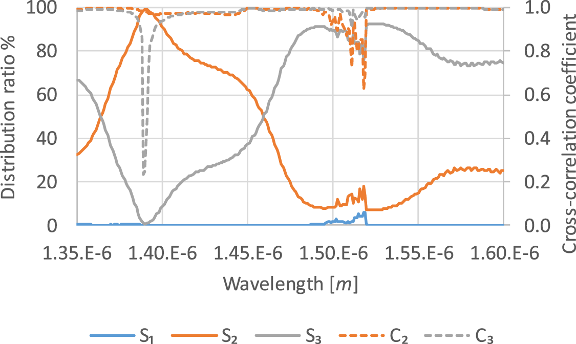
Subsequently, the cases for E0 = 1.0 [V/m] and 1.5 [V/m] were simulated. Figure 6 depicts the distribution ratios for ports 1, 2, and 3 and the cross-correlations between ports 2 and 3 for E0 = 1.0 [V/m]. The changes in the ratio of distribution and cross-correlation in vicinity of λ = 1.500 [µm] are more pronounced than those for E0 = 0.5 [V/m].
Distribution ratio of port 1, port 2, and port 3 and cross-correlation coefficient of port 2 and port 3 for
Figure 7 depicts the electric field profiles for λ = 1.389 [µm] and λ = 1.518 [µm]. Figure 8 presents the distribution ratios for ports 1, 2, and 3, and the cross-correlation coefficient between ports 2 and 3 for E0 = 1.5 [V/m]. The variations in the distribution ratio and cross-correlation coefficient around λ = 1.500 [µm] are greater than those for E0 = 1.0 [V/m]. Figure 9 shows the electric field distribution at wavelengths λ = 1.392 [µm] and λ = 1.516 [µm]. These results indicate that the distribution ratio and cross-correlation coefficient increase significantly with increase in the input amplitude.
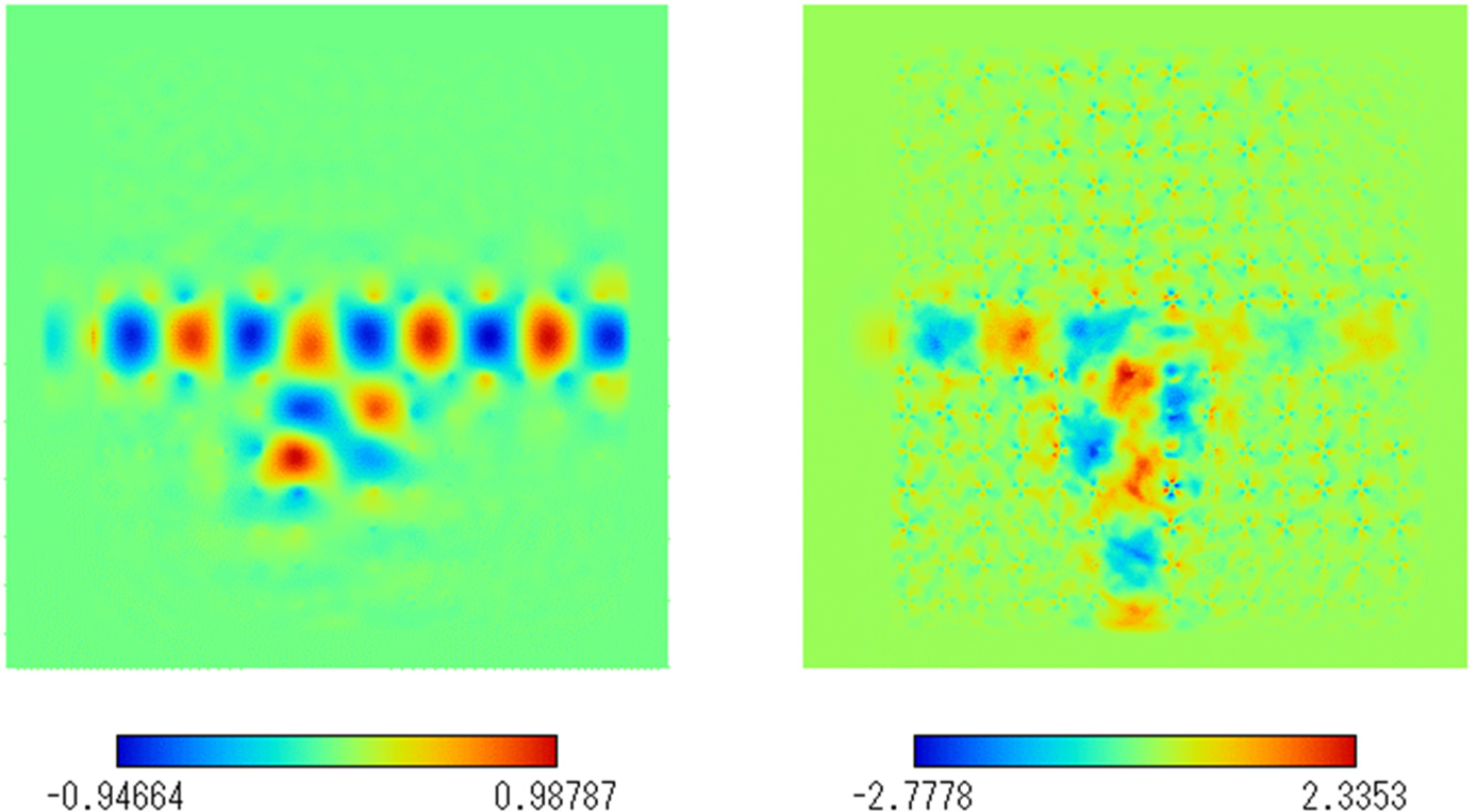
Electric field distribution at
Distribution ratio of port 1, port 2, and port 3 and cross-correlation coefficient of port 2 and port 3
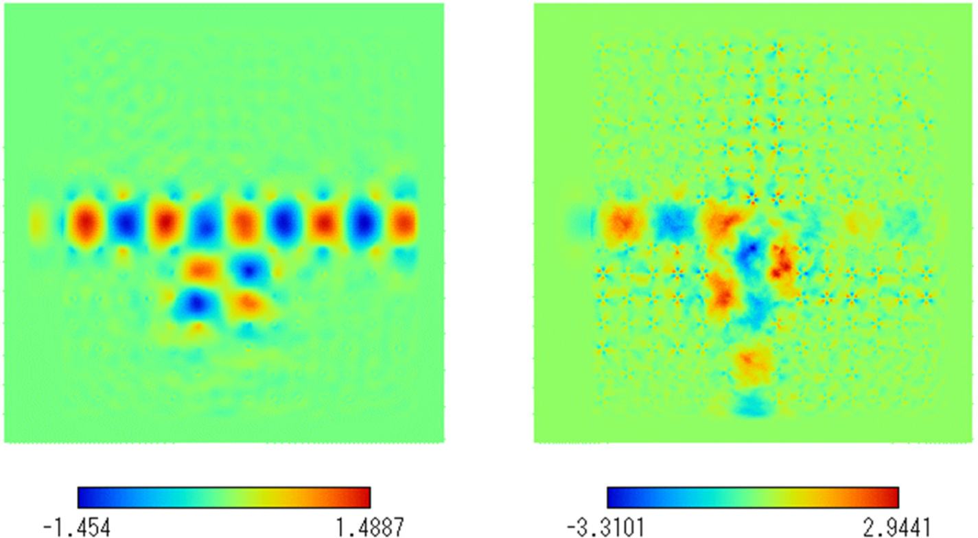
Electric field distribution at
This phenomenon can be explained as follows: When the input electric field amplitude is too large, it is thought that the refractive index changes due to self-index modulation, a nonlinear optical effect, and becomes significant. This causes the periodic variation of the refractive index to collapse in the vicinity where a large optical amplitude exists. As a result, it was found that the confinement of the optical field by the photonic bandgap no longer occurs.
Table 2 summarizes the power spectra at the main output port and the remaining output ports when input signals with two representative wavelengths are given. They are normalized by the power spectrum at the main output port. Table 2(a) compares the output levels at ports 2 and 3 for wavelengths of 1.388 µm and 1.516 µm when the input signal amplitude is E0 = 0.1 [V/m]. The second and third rows of the table summarize whether other power spectra are observed. According to the results, the wavelength of 1.388 µm achieves a normalized power spectrum of 1.0 at port 2, while it is 0.029 at port 3. The extinction ratio in this case is approximately 15.4 dB. For the wavelength of 1.516 µm, the normalized power spectrum is 1.0 at port 3, while it is 0.255 at port 2. The extinction ratio in this case is approximately 5.93 dB. No other wavelength components are observed.
Normalized output power spectra for typical input signals.

Next, Table 2(b) shows the results when the input signal amplitude is E0 = 1.5 [V/m] and the input wavelengths are 1.392 µm and 1.516 µm. When the input amplitude is large, the effects of the nonlinear dielectric constant of SiO2 become apparent. For the wavelength of 1.392 µm, a normalized power spectrum of 1.0 appears at port 2, and nearby wavelength components also appear at ports 1 and 3. Additionally, multiple harmonic components of various orders appear at all ports. For the input signal with a wavelength of 1.516 µm, a normalized power spectrum of 1.0 appears at port 3, and the same wavelength component appears at port 2 with a value of 0.349. Multiple harmonic components of various orders also appear at all ports. It is evident that when using SiO2, it is necessary to keep the input amplitude sufficiently small to minimize the effects of nonlinear optical phenomena.
Finally, the variation in the radius of the silica pillars (a total of eight green pillars in Figure 1) as a duplexer was examined to tune the output frequency to port 2. Table 3 lists the maximum power distribution ratio to port 2 as a function of the radius R of the green pillars. The magnification ratio is expressed as R/Rλ = 1.389 µm, where the radius of the pillars for λ = 1.389 µm is the reference value. This relationship is also plotted against the magnification ratio in Figure 10. From the table and the figure, it was observed that this structure exhibits tunable transmission characteristics to port 2. This feature is applicable for demultiplexing WDM signal systems to drop or add a signal of specific modulation wavelength.
Power distribution ratio to port 2 as a function of wavelength and radius of silica pillars of duplexer at T-shaped branch point in Figure 1.

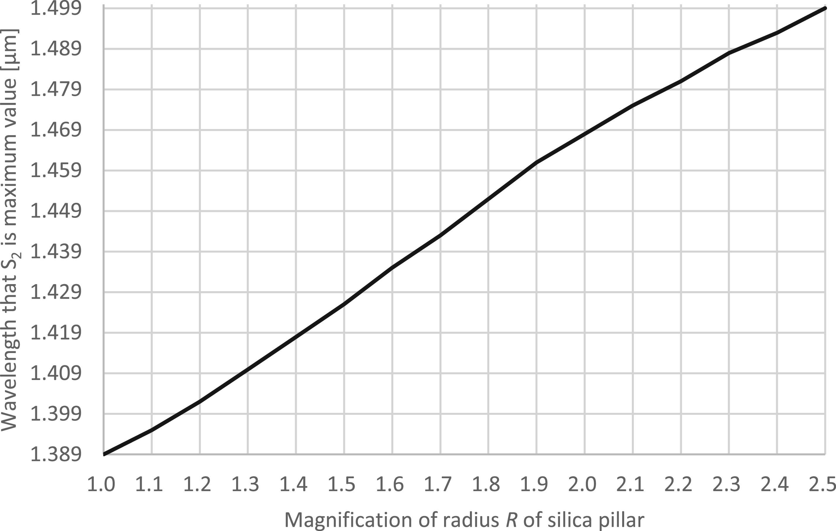
Output wavelength to port 2 as a function of magnified radius R of six pillars at branch point.
To consider a signal add/drop circuit for a WDM system, let us examine cascaded circuits with different magnified radii R, as shown in Table 3. In the first stage of the cascaded circuit with a magnification of 1.0, only the signal with λ = 1.389 [µm] is transmitted to port 2, serving as the dropped or demultiplexed output signal. The other frequency components are primarily transmitted to port 3 and proceed to the second stage of the cascaded circuit. In the second stage, with the magnification of the duplexer pillar radius set to 2.0, the signal with λ = 1.468 [µm] is transmitted to port 2 of the second stage as the dropped output signal. By increasing the number of cascaded stages in an optical IC, multiple channels can be multiplexed and demultiplexed within a monolithic structure. This approach offers significant advantages for the realization of optical signal exchange with high functionality, high stability, and low power consumption due to passive circuits, and cost reduction through mass production, similar to semiconductor ICs.
Regarding high-density photonic ICs, Pérez et al. 24 report experiments where Mach–Zehnder interferometers or ring resonators are connected in a mesh configuration. As previously mentioned, photonic crystal structures consist of simple repeating unit cells, making them suitable for constructing large-scale photonic ICs. Like Pérez et al., 24 by incorporating waveguide structures formed by defect lines into large-scale photonic ICs based on photonic crystal structures, it is considered feasible to fabricate large-scale circuits with multi-stage connections of the proposed circuits. Specifically in the proposed circuit, let us consider the case where circuits with varying silica radii in the duplexer are connected in multiple stages. The wavelength components dropped by the duplexer in the first stage are output to port 2, while the others are guided to port 3 and then to the second stage. In the second stage, by setting the radii of the duplexer differently from the first stage, different wavelength components are dropped. By repeating this process, it is possible to extract the desired wavelength components from the desired ports. By pre-assigning the wavelengths of light to the network routing information, the optical envelope pulse train representing the optical packet will be output to specific ports. By connecting these stages in series, passive routing of optical packets can be achieved.
In this study, a resonator made of Si and fused SiO2 is installed at the branch point of a two-dimensional photonic crystal waveguide to function as a duplexer. The following is a summary of the results.
The distribution characteristics based on changes in the amplitude and wavelength of the input signal are analyzed using a frequency-dependent FDTD method. By designing the diameter of the silica pillars, it is possible to adjust the wavelength of the add/drop signals. The contributions of this research include:
It is based on a photonic crystal structure suitable for the realization of photonic ICs. The material used is quartz glass, which is also used in optical fibers, indicating high compatibility with future photonic networks. The design of a passive optical packet routing circuit and the verification of its performance through simulations. The variations in the distribution ratio and cross-correlation coefficient for input electric field amplitudes E0 = 0.1, 0.5, 1.0, and 1.5 [V/m] were observed, confirming that E0 = 0.1 [V/m] is the optimal input amplitude.
The following are future challenges. When the proposed structure is connected in multiple stages, it is necessary to confirm that signals with different modulation wavelengths are output from each stage when the radius of the cylinders composing the duplexer is varied for each stage in response to WDM input. At that time, it is also required to calculate the extinction ratio of the multiplexed signal after the desired wavelength components have been dropped.
Finally, we discuss the outcomes of this study and their relevance to future information networks implementing all-photonic routing technology. The all-photonics network (APN), part of NTT's IOWN initiative, 25 leverages optical technology to achieve low power consumption, high-speed large-capacity communication, and low latency. This enables innovations in areas such as inter-data center communication, telemedicine, and broadcasting. APN plays a crucial role as the foundation for a sustainable and efficient future communication infrastructure. The circuit proposed in this study is a passive type that does not consume power for path control, and it is capable of extracting only the light pulse signals modulated at the desired wavelength to the output port, depending on the wavelength of the light. This suggests that it contributes to the realization of the APN.
Footnotes

Funding
The author received no financial support for the research, authorship, and/or publication of this article.
Declaration of conflicting interests
The author declared no potential conflicts of interest with respect to the research, authorship, and/or publication of this article.