



Abstract
Defects in solar cells can be caused during processing or through a benign event like a falling leaf when operating in an outdoor system. Shading caused by such a leaf can result in the cell operating in the reverse direction and ultimately in hotspot formation, which in turn can cause the entire cell to breakdown and essentially become a power dissipator rather than a producer. More often than not, this reverse biasing of the cell will enhance the effect of any inherent defect. In this study, poly-Si cells were reverse biased to enhance the effect of their inherent defect. These defects were then analysed using non-destructive confocal Raman spectroscopy, since this technique allows us to observe small defects in cells/material using the intensity of the transverse optic bands. The intensity of defect-induced Raman band has a direct relationship with the observed morphological defects of the reverse biased cell. The quality of the active layer was also investigated; this includes the chemical composition and the stress level which can be found through the single spectrum bandwidth. The efficiency of solar material depends on the absorption capability of the solar material, while the optical and the electrical properties to a large extent determine the absorption capability of solar cell. However, its structure, defect and stress level can offset the total optical and electronic properties. The present study reveals defect in micro-level and the stress induced in the affected region of the solar cell. Confocal Raman is suitable for characterising stresses in relation to microstructure, defect level as well as the manufacturer-induced defect in the substrate.
Introduction
This study is born out of the need to provide experimental contribution to the vibrational behaviour as well as the structural property of polycrystalline silicon solar cell (poly-Si). Unlike the theoretical investigation of poly-Si vibrational properties that has created great interest among researchers, over the past 40 years, 1 little has been done on the experimental investigation. Majority of the theoretical studies that have been done were only concerned with the qualitative comparisons of the vibrational density of states of the structural models. 1 In terms of quantitative investigation, there are a handful of papers that relate the structural to vibrational properties, but most of these studies are theoretical studies.2–5 Having a good knowledge of the quantitative relationship between the structural and vibrational properties is very important. This is because it is useful for relating the structural properties and vibrational properties to the spectrum width (linewidth) of the spectrum transverse optic Raman peak, as well as the extent of disorderliness.6–9 This is an effective approach in characterising the defect level of the sample when using confocal Raman microscope. The width of the band is influenced to a large extent by the coordination defects localised in such spot.10,11 In this present work, Raman spectra were used to qualitatively and quantitatively diagnose poly-Si. The qualitative evaluation of the spectra linewidth of the transverse optic Raman peak was used to analyse the degree of defect and the stress. The basic images were used to investigate the structural properties of both the affected and the non-affected regions. Raman spectroscopy is a well-suitable method for photovoltaic (PV) analysis because of the nature of silicon–silicon bond. Silicon–silicon bonds are known to be symmetrical and produce strong Raman scattering which makes it easy to study any variations that might occur. In addition, crystalline silicon has highly ordered structure, bond angle and bond length; at a wavelength of 521 cm−1, it exhibits a sharp Raman peak. The relevance of this study lies in the use of both qualitative and quantitative analysis to study the effect of degradation, to reveal the effect of degradation and its associative defects on the acquired Raman spectra. The technique gives a direct approach in addressing the issues of long-term degradation issues resulting from defect.
Research methodology
Three poly-crystalline solar cells of 156 mm × 156 mm dimensions with 2 busbar and 200
Results and discussion
Defect analysis
The large area scan presented in this section was done on the area indicated by the red rectangular box in Figure 1(a). The level of defects in the sample can be estimated from their Raman intensity of the Si peak. A high degree of defect decreases the Si peak in the case of deep impurities. The degree of defect in the samples has been studied from single Raman spectra acquired from combined images of both the affected and non-affected regions. The appearance of other peaks in the spectrum is an indication of the defect caused by elemental impurities. Under the same measurement condition, the single spectra acquired from pure samples are expected to have uniform intensities, but the presence of defect affects the intensity of a particular chemical bond, in this case Si–Si tetrahedral bond as shown in Figure 2.

Large area scan of reverse biased poly-Si cell showing the: (a) stitching image. (b–e) Drawn images representing different phase distribution of chemical impurities. (f) Combined image of different distributions indicating the existence of different phases.

Different spectra indicating the existence of five different phases at the surface of the sample; this gives the corresponding five colour codes.
The stitching image was used to identify the location of the defects, Figure 1(a), and the light red rectangular box region was further scanned so as to give a detailed information about the defect. Four different drawn images resulted from the scanned area and each of them is displayed in Figure 1(b) to (e). The difference in each image is displayed in their colour codes, which helps to identity the different elemental impurities, present in the defective area. The combination of the various colour codes resulted to the combined image presented in Figure 1(f). The data acquired from the various drawn images in Figure 1 provide the Raman spectra of the analysed sample; this is presented in Figure 2.
The data extracted from the combined image are analysed in Figure 2. Each of the colour code represents a particular spectrum presented in Figure 1(f). In Figure 2, it is clear that only the red spectrum contains Si peak, while the other spectrum contains a different element which differs from Si, and hence they are acting as impurities. It is important to note that only the sample with defective cluster is analysed in Figure 2, hence the low quantity of Si.
As stated earlier, the spectra acquired from the combined basic images are given in Figure 2. The concentration of each measured spectrum is defined by the intensity of the Raman peak, which is defined by equation (1)13–15

The temperature-dependent factor is a function of the spectral width, system resolution detector and mechanical properties of the analysed sample. In the defect-free region of the sample, the silicon bond vibration corresponds to the red spectrum which peaks at 525 cm−1 as represented in Figure 2. However, Si Raman peak is theoretically given as 520 cm−1 but in this study, the three known Si phonon Raman peaks degenerated at 525 cm−1 due to the Si reference used as observed during the calibration process. Hence, 525 cm−1 is used for Si in this study. Generally, Si has vibration modes at spectra line of 300 cm−1, 520 cm−1 (narrow line) and overtone at 940 cm−1.13,14 The higher and broader peaks in Figure 2 correspond to the forbidden transverse optical peaks, which are not the characteristics of any of the known three basic Si phonons; hence, they represent impurities.
In addition, from Figure 2, the first-order Raman spectrum of the poly-Si reveals extra phonon frequencies more than the theoretically recognised ones for crystalline solar cells. Apart from Si Raman peak that is normally present between 518 cm−1 and 525 cm−1, the other observed bands, 78 cm−1, 227 cm−1 and 1300 cm−1, are attributed to impurities due to defects at the region where total junction breakdown occurred. The presence of unusual vibrational mode also appears at 288 cm−1 due to co-implantation of oxygen (O) in the defected region and this is possible because of the high O content associated with hotspot centre.15,16
FHWM analysis of different regions
The origins of Raman shift emanated from shift in the bond-to-bond vibrational frequency induced due to strain or stress in the analysed sample. The interatomic vibrational alteration is best identified via Raman spectroscopy to show the distribution of stress across the material.17,12–14,18 In analysing the degree of shift experienced in this study, Gaussian line was used to analyse the spectra in order to have the best analysis. This theory is based on experimental test observed during the analytical part of this work and this agrees with the work of Anastassakis. 18 Although a combination of Gaussian–Lorentzian shape could also yield a good analysis, the complexity surrounding the method due to additional fitting parameters makes this method less attractive.19–21 Figure 3 indicates the Raman shift experienced by the spectra from the affected and the non-affected regions. Note that the affected spectrum is presented with a red line, while the region outside the affected region is presented in black. The inserted spectra in Figure 3 are the actual spectra before applying fitting; thus, the inserted spectra are the main spectra of the analysed sample.
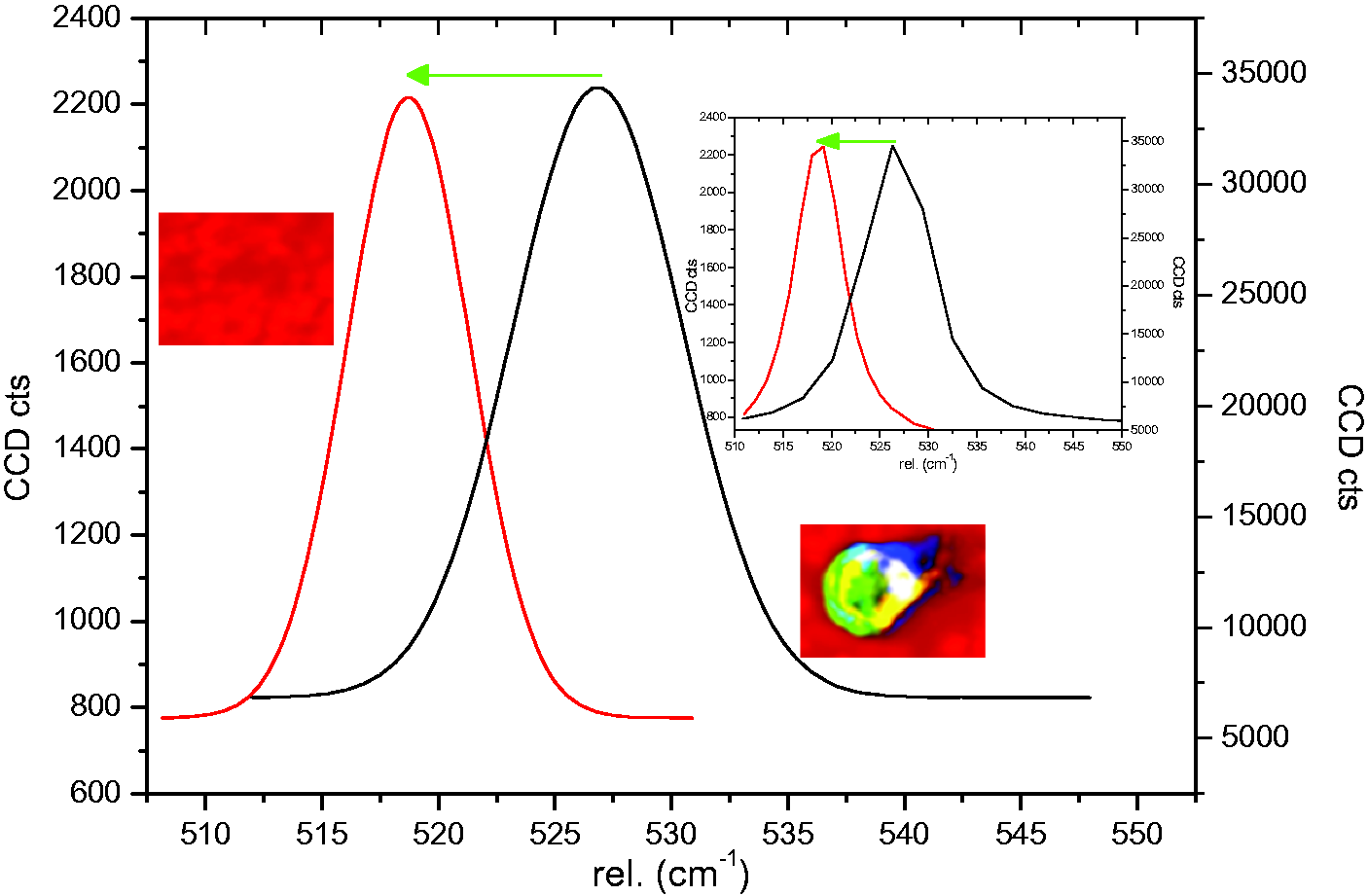
Qualitative analysis of stress/strain in and outside the defective region using FWHM, showing a shift in the Raman peak from 525 cm−1 to 518 cm−1 and a decrease in the spectrum width as a sign of low quality.
The most significant observation is the shift in the Raman peak from high to low frequency due to strain and decrease in the spectrum width. The decrease in the bandwidth is a sign of low material quality in the defective region; this can be attributed to the high concentration of impurities observed.
Deep level analysis
From single Raman spectra, it is clear that the defect resulted from elemental impurities, but the depth of impurities could not be determined; hence, there is a need for depth profiling. The section of the sample analysed in Figure 1 was further subjected to deep level scanning to ascertain the depth of the defect cluster. The depth analysis shows that the impurities in the defected centre as seen in the Raman spectra are not surface contaminations, rather a deep level impurity defects. The influence of tensile stress in the material active layer resulted to the precipitation of the moonlike defect, which has been addressed as the defective cluster in this study. The deep level scan of the defect cluster is presented in Figure 4. The blue line in Figure 4(a) indicates the spot where the deep level scan was performed, while Figure 4(b) to (d) show the different drawn images; the combined image is shown in Figure 4(e).
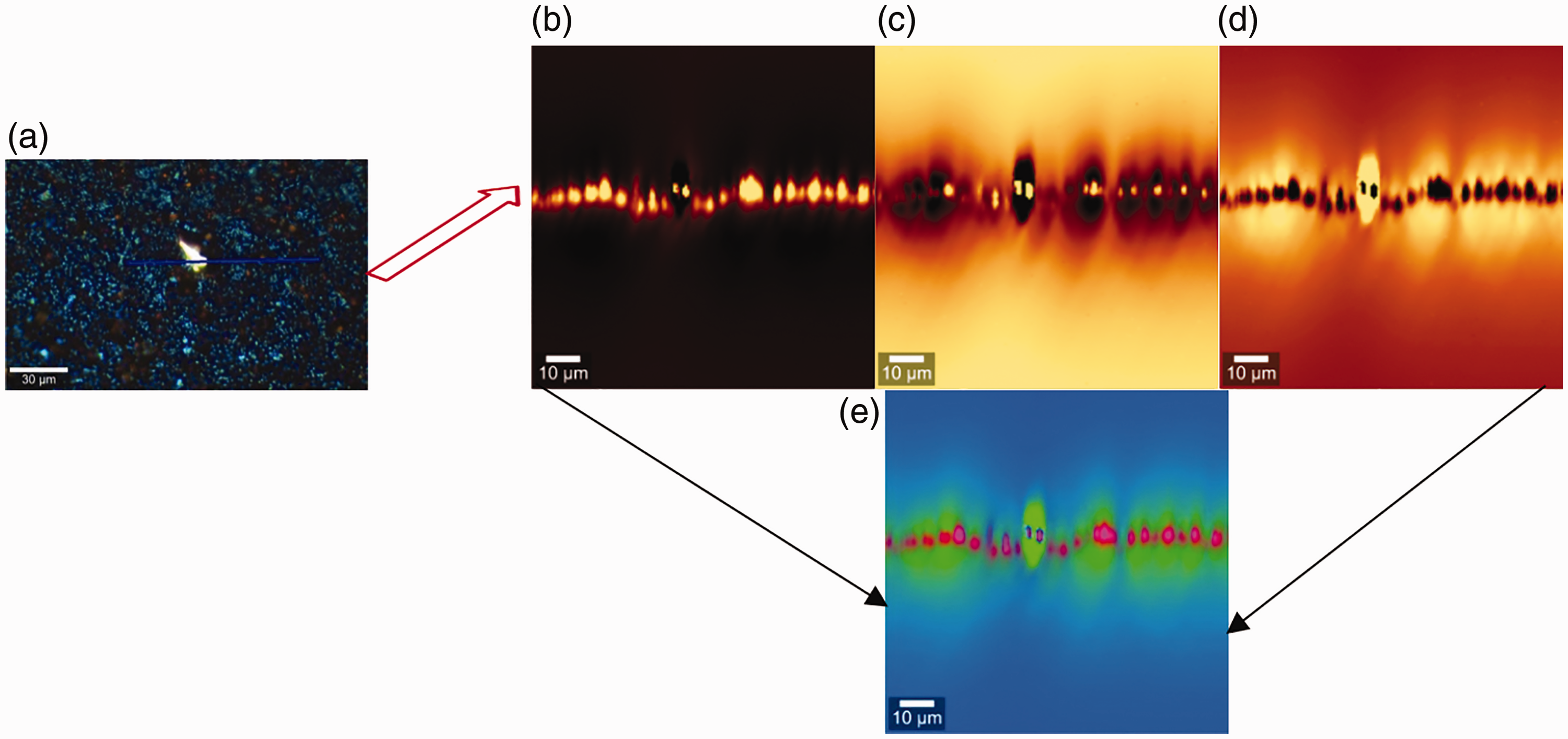
Large area scan of a reverse biased poly-Si cell showing the depth profiling of the defective cluster region. (a) The optical image. (b–d) The drawn images. (e) The combined drawn image.
As stated before, the aim of the depth scan measurement was to investigate how deep the defect is in the sample substrate. Figure 4 shows an in-depth profile of the defected cluster which is acting at contaminants. This profiling was made possible because the sample matrix is transparent to the incoming laser. The position identified was manually focused and the resulted images show the distribution and origin of the defect. The profile reveals that the contaminants have high concentration at the middle as seen from the distribution. The depth profiling gave detail information about the defect; this technique work on the principle of optical sectioning by improving the aperture lateral and axial spatial resolution of the device; hence, depth profile data are acquired in an incremental order deep into the material. This helps eliminate the possibility of sample contamination, since no extra preparation is needed.
The depth profile image shows that there are three distinct elemental impurities that constitute the defective cluster. The fourth impurity observed from the spectra presented in Figure 2 is a metal substance, while the fifth is purely silicon, which is the parent element of the solar cell. The depth scan also confirms the various concentrations that resulted to the difference in the intensity signal resulting from Raman spectra.
Conclusion
The application of confocal Raman spectrometer in characterising defects in poly-Si solar cell has been demonstrated. This paper revealed the effect of impurity on the defect level of poly-Si solar cell. Raman spectra show that the observed moonlike defect clusters originated from high concentration of chemical impurities. The precipitation of this defect cluster is attributed to hotspot formation which was enhanced during the reverse biasing process. The changes in the Raman peaks and the presence of other peaks show the presence of impurities in the analysed sample. In this study, FWHM analysis was used to quantify the stress level in the affected region, and it was observed that the interatomic bonding of the defected region experiences strain because the Raman shift moves towards the strain level compared to the stress position. The changes in the single spectra widths and variation in the intensities made it possible to probe the defect level and the nature of the stress.
Footnotes
Declaration of conflicting interests
The author(s) declared no potential conflicts of interest with respect to the research, authorship, and/or publication of this article.
Funding
The author(s) disclosed receipt of the following financial support for the research, authorship, and/or publication of this article: We are grateful for the financial support from our sponsors South African National Research Foundation (NRF), DST, and Govani Beki Research & Development Centre (GMRDC) of the University of Fort Hare.