
Abstract
This study investigates the influence of system configuration single-layer, composite, and bilayer on the structural, morphological, and optical properties of TiO2-ZnO thin films. Four different structural designs were fabricated using the sol–gel spin-coating method: TiO2, ZnO, TiO2:ZnO composite and ZnO/TiO2 bilayer. Structural analysis revealed that the ZnO/TiO2 bilayer exhibited characteristic diffraction peaks corresponding to both crystalline oxides, confirming the formation of a dual-phase heterostructure. However, the TiO2: ZnO composite film does not exhibit discernible Bragg reflections within the scanned 2θ range. The single layer TiO2 and ZnO films displayed the expected anatase (101) and hexagonal (100) and (002) crystallographic orientations, respectively. Surface morphology analysis indicated apredominantly compact and relatively smoothfor TiO2. The ZnO Several elongated surface features with lateral dimensions of ∼ 954 nm, 981 nm, and 1009 nm are observed. These features may correspond to coalesced grains or preferentially oriented growth structures formed during thermal treatment. All thin film configurations exhibited high optical transparency exceeding 60% in the 350–900 nm wavelength range. The optical band gap values varied with film configuration, ranging from 3.52 to 4.13 eV. The ZnO/TiO2 bilayer showed the lowest band gap value (3.52 eV), which can be attributed to interfacial interactions at the heterojunction.
Introduction
In recent years, thin film technology has attracted significant attention due to its extensive applications in optical, electronic, and optoelectronic devices. Although single-layer thin films have become increasingly prevalent, many modern applications necessitate multilayer thin films that integrate the properties of various materials. Such multilayer structures are frequently employed in the fabrication of optical reflectors, computer storage media, anti-reflective coatings, and solar cells. 1 Studies indicate that layering two semiconductors can enhance optical and electrical properties due to their synergistic interactions.2,3
Metal oxide thin films, particularly titanium dioxide (TiO2) and zinc oxide (ZnO), are extensively studied due to their unique optical, electronic, and structural characteristics, making them suitable for photocatalysis, photovoltaics, gas sensors, and transparent electronics. However, the intrinsic properties of these semiconductors differ, with ZnO having a direct energy bandgap and TiO2 possessing an indirect energy bandgap. 4 Both TiO2 and ZnO thin films exhibit high transparency in the visible spectrum, chemical stability, and adjustable band gaps, allowing performance optimization according to application-specific requirements.
TiO2, a well-known n-type semiconductor with a band gap of approximately 3.2 eV, 5 is highly valuable for UV-responsive applications such as photocatalysis and gas sensing. Although undopedTiO2 is transparent and stable, its limited visible-light absorption restricts its broader applicability. Strategies to improve TiO2 performance include doping or forming composites with other metal oxides to extend its optical activity into the visible range and enhance photocatalytic efficiency. ZnO, another metal oxide semiconductor with a comparable band gap (∼ 3.37 eV), is distinguished by its high electron mobility,6,7 strong exciton binding energy, and piezoelectric properties, making it ideal for optoelectronic devices, sensors, and energy-related applications. Similar to TiO2, undoped ZnO predominantly absorbs in the UV range, yet its transparency, stability, and electronic properties make it suitable for transparent conductive oxides and robust device performance.
Numerous techniques have been utilized to deposit ZnO and TiO2 thin films, including spray pyrolysis, 8 sol–gel methods, 9 and chemical vapor deposition. 10 Among these, the sol–gel method stands out as an affordable technique that facilitates low-temperature synthesis while providing excellent control over film purity and uniformity. 5 Combining ZnO and TiO2 in a 50% mixed-metal oxide structure leverages the advantages of both materials. This composition enhances optical properties, extends light absorption across the UV-visible spectrum, and potentially improves photocatalytic efficiency. Mixed metal oxides, such as the 50% (TiO2:ZnO) composition, are anticipated to improve charge separation, increase catalytic surface area, and enhance photocatalytic and optoelectronic performance, beneficial for environmental and energy applications. 11
The ZnO/TiO2 bilayer thin film structure offers an alternative approach, sequentially depositing the two oxides to form an interface that improves charge separation, extends carrier lifetimes, and reduces recombination losses. This bilayer arrangement is particularly advantageous for photovoltaic and photocatalytic applications, where efficient charge transfer between ZnO and TiO2 significantly enhances performance compared to individual or mixed-metal films. ZnO/TiO2 bilayers thus demonstrate considerable promise for applications demanding superior optoelectronic characteristics. 5
To the best of our knowledge, no comparative studies have been conducted on TiO2, ZnO, (TiO2:ZnO) mixed thin films, and ZnO/TiO2 bilayer thin films deposited on glass substrates. Therefore, this study investigates ZnO/TiO2 bilayers synthesized via the sol–gel spin-coating method, comparing their crystalline structure, morphology, and optical properties.
Experimental Details
Materials and Methods
Synthesis of TiO2 Films
The process for synthesizing TiO2 films begins with the addition 2.8 ml of TTIP (Titanium tetraisopropoxide) (Ti(OCH (CH3)2)4) (+97% purity) to 2 ml of isopropanol (CH3CHOH CH3) (99.99% purity) which were added drop by drop, under vigorous magnetic stirring for 10 min at room temperature, 3.2 ml of acetic acid (CH3COOH) (99.99% purity) is then introduced, and the mixture is stirred for another 15 min. After that, 10 ml of methanol was added, and the stirring continues for an additional hour. The sol obtained is subsequently deposited onto cleaned glass substrates using a spin coating method at 2000 r/min for 30 s per layer.
Each layer undergoes preheating at 120 °C for 10 min to evaporate the solvent. This spin coating process is repeated for a total of five times. Finally, the films are annealed at 500 °C for 90 min in a Nabertherm muffle furnace.
Synthesis of ZnO Films
ZnO films were synthesized using the sol–gel method. Zinc acetate dihydrate (C4H12O6Zn-2H2O) (99.99% purity) was used as the zinc precursor and dissolved in methanol under magnetic stirring, 2 ml of Diethanolamine (DEA) (C4H11NO2, 98% purity) was used as a catalyst. The solution was stirred until a clear and homogeneous sol was obtained. The films were deposited using the same spin-coating parameters described above, followed by drying at 120 °C for 10 min after each layer
Synthesis of TiO2:ZnO Composite
The TiO2: ZnO composite sol was prepared by mixing the previously prepared undoped TiO2 and ZnO in a 1:1 volume ratio under magnetic stirring for 1 h to ensure complete homogenization. The composite films were deposited by spin coating at 2000 r/min for 30 s per layer. After each deposition, the films were dried at 120 °C for 10 min. The coating process was repeated five times to obtain the desired thickness. Finally, the films were annealed at 500 °C for 90 min to improve their structure and optical properties. We mixed the prepared undoped TiO2 solution with the undopedZnO solution in a 1:1 volume ratio.
Synthesis of ZnO/TiO2 bilayer
Undoped TiO2 and ZnO thin films were first prepared as described above. TiO2 layer was initially deposited onto the cleaned substrate by spin coating at 3000 rpm for 30
Characterization of sol-gel ZnO-TiO2Thin films
The crystal structure of the films was analyzed using X-ray diffraction (XRD) with a D8 Advanced Bruker AXS θ–2θ diffractometer, where CuKα of wavelength λ = 0.15406 nm was employed for the radiation, and the diffraction patterns were measured within the 2θ range of 20° to 80°.The samples’ surface morphology was analyzed by Scanning Electron Microscopy (SEM) using a (Jeol JSM-6360LV);the system was equipped with secondary and backscattered electron detectors, along with digital image capture capabilities and atomic force microscope (AFM). The elemental composition of the films was analyzed using SEM/EDS, incorporating a Bruker quantax energy-dispersive X-ray spectrometer. The optical transmittance of the thin films was measured at ambient temperature using a Shimadzu 3101 PC UV-visible spectrophotometer, and the FTIR spectra of the films were recorded using a Fourier transform infrared spectrometer (Nicolet Avatar 360).
Results and discussion
Structural Analysis
The crystal structures of TiO2, ZnO, TiO2:ZnO thin films, and ZnO/TiO2bilayer thin films were analyzed using X-ray diffraction (XRD) to determine their phases and crystallinity. The diffraction pattern of TiO2 reveals the presence of the anatase phase


XRDspectra of tdeposited thin films.
Where λ represents the X-ray wavelength (1.54056 Å), θ denotes the Bragg angle of diffraction,the constant k is the shape factor (usually taken as 0.9), and β corresponds to the full width at half maximum (FWHM) of the peak at that specific angle θ.
δ Describes the dislocation density,which determines the length of dislocation lines within the crystal per unit volume.7,21

The FWHM values for the peaks at 25.15°, 31.35°, and 31.50° were 0.024, 0.0119, and 0.0165 for TiO2, ZnO, thin films, and TiO2/ZnO bilayer thin films, respectively. The corresponding crystallite sizes were 5.77, 11.65, and 8.4031 nm. As shown in Table 1.
Extracted XRD parameters corresponding to Figure 1.

Raman analysis
Raman spectroscopy is a highly sensitive technique for analyzing the crystal structure and phase of TiO2 and ZnO without causing any damage to the material. 5 The chemical bonding in ZnO is intermediate between ionic and covalent. The bond ionicity between Zn and O atoms is relatively high (about 0.62 on the Phillips scale), which is why they are commonly represented as Zn + 2 and O−2 ions. Under ambient conditions, ZnO typically adopts a thermodynamically stable hexagonal wurtzite structure. When ZnO is deposited on cubic substrate, it can also exhibit zinc-blende structure, respectively. 22 Using excitation at 532 nm,as shown in Figure 2, prominent Raman shifts are evident from the distinct peaks that appear 396, 559, 639, and 797 cm−1 confirmed Eg,B1g,A1g, and Eg phonon vibrational modes of the anatase TiO2 phase in lattice respectively. 22 ZnO Thin films characterized by a hexagonal wurtzite structure and excellent crystallinity exhibit a peak at approximately 1101 cm−1 and exhibit higher intensity and narrower line-width, corresponding to a 2LO phonon mode process. Similar to Zhuo, R, et al.. 23 Findings, excitation by laser lines at 325 nm indicates dominance of the 1 LO and multi-LO modes.The intensity of the bands increases notably when comparing the ZnO/TiO2 bilayer thin films (554 cm−1 and 790 cm−1) to those of ZnO monolayer thin films. Additionally, in this case, the intensity of the main band is significantly elevated at 2820.35 cm−1. Below 1000 cm−1 was attributed to the Ti–O–Ti bond stretching vibrations in TiO2. Therefore, the Raman spectra of the TiO2:ZnO composite and ZnO/TiO2 bilayer films exhibit vibrational features associated with phonon vibrational modes and Ti–O and Zn–O bonding environments. However, since Raman spectroscopy probes short-range structural order, these features indicate local structural organization or partial crystallinity rather than conclusively demonstrating fully developed long-range crystalline phases.

Raman spectraof thin films: (a) TiO2. (b)ZnO. (c) TiO2:ZnOcomposite and (d)ZnO /TiO2 bilayer.
FTIR analysis
FTIR is an effective method to analyze the composition of compounds or products. The FTIR spectra of the films were obtained using a FTIR (Nicolet Avatar 360) in the range of 400-4000 cm−1. Metal oxides often show characteristic absorption bands in the fingerprint region (below 1000 cm−1), which are ascribed to vibrations between atoms. 24 Figure 3 shows the FTIR spectrum of TiO2, ZnO,TiO2:ZnO composite, and ZnO/TiO2 bilayers thin films. For the TiO2 thin film, the strong absorption band observed in the 450–600 cm⁻1 region is attributed to Ti–O–Ti lattice stretching vibrations, characteristic of the TiO2 network structure. 25 A band around ∼1630 cm−1 is assigned to the H–O–H bending mode of molecularly adsorbed water and Ti–OH surface groups, 18 which commonly appear in sol–gel derived oxide films due to surface hydration. 26 These results well agree with earlier.27,28 A weak absorption feature was observed around ∼2105 cm−1, Vibrational modes in the 2100–2200 cm−1 region are typically associated with C≡C, C≡N stretching vibrations, or adsorbed CO species on oxide surfaces.29,30 However no precursors containing triple bonds(C≡C or C≡N) were used in the present synthesis, and no complementary evidence supports the presence of such functional groups, therefore, this weak band is cautiously attributed to (CO related adsorption). For ZnO thin films, Zn–O stretching vibrations are expected below ∼600 cm−1. The broad absorption features observed in the 400–600 cm−1 region are therefore assigned to Zn–O lattice vibrations. Bands appearing in the 1400–1600 cm−1 region are attributed to surface carbonate species or residual organic fragments resulting from atmospheric CO2 adsorption or incomplete removal of organic residues during annealing. 26 The TiO2:ZnO composite and ZnO/TiO2 bilayer thin films exhibit similar spectral characteristics, which is expected due to the common presence of metal oxygen frameworks and surface hydroxylation effects. FTIR spectroscopy confirms the formation of metal oxygen bonds in all films, however, it is not highly phase-selective for distinguishing crystalline phases. Therefore, phase identification and crystallinity are primarily supported by XRD and Raman analyses, while FTIR provides complementary information regarding chemical bonding and surface chemistry.31,32

FTIR spectra ofdeposited thin films.
AFM analysis
Atomic Force Microscopy (AFM) operated in tapping mode offers comprehensive insights into the surface morphology and nanoscale topography of thin films. This method allows for precise quantitative evaluation of parameters such as grain size, shape anisotropy, height distribution, and Root Mean Square (RMS) roughness, all of which are essential for analyzing film growth dynamics and defect formation.30,31
Figure 4. shows the 2D and 3D topographic of thin films. As observed, the morphology of the TiO2 films exhibits an RMS roughness of approximately 2.27 nm.
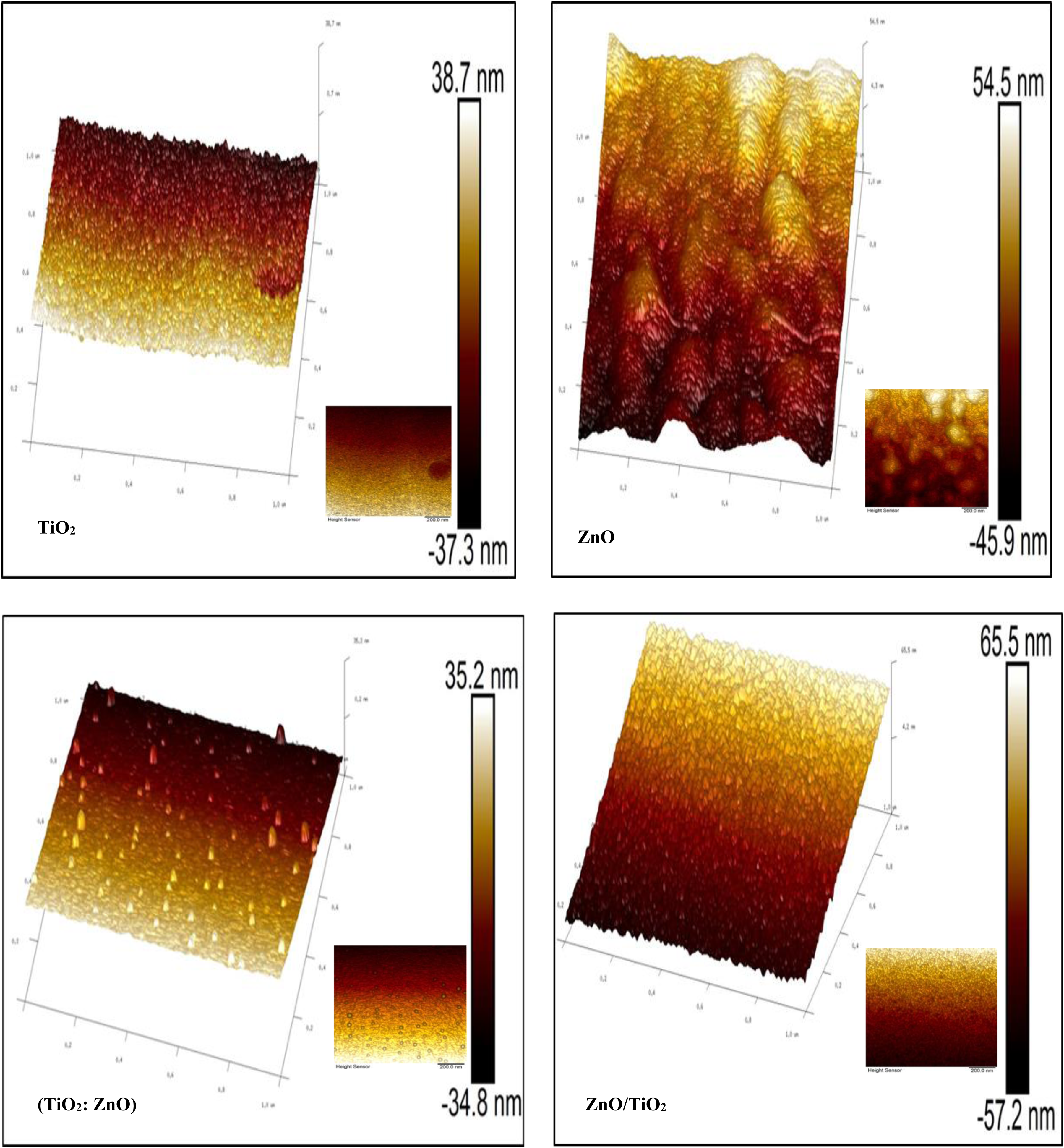
Morphology and surface roughness of: TiO2, ZnO, (TiO2: ZnO), and ZnO/TiO2 thin films.
Surface morphology
Figure 5. shows SEM micrographs of the spin coating TiO2, ZnO, TiO2:ZnO compsite, and ZnO/TiO2 bilayer thin films. Magnifications ranging from 50,000× to 80,000× were employed to provide an in-depth view of the thin films. The TiO2 thin film Figure 5(a) exhibits a predominantly compact and relatively smooth surface. However, localized micro-cracks and small particle agglomerates are also visible. Such micro crack networks are commonly attributed to shrinkage induced tensile stress during solvent evaporation and densification in sol gel derived films, or annealing at 500 °C process.5,35 Despite these localized defects, the overall surface morphology remains continuous and uniform. The ZnO thin film Figure 5(b) appears largely continuous and compact, but contrast variations are observed across the surface. These variations may arise from local differences in surface topography, grain orientation, density fluctuations, which are frequently encountered in SEM analysis of oxide films deposited on insulating substrates.
36
Several elongated surface features with lateral dimensions of ∼ 954 nm, 981 nm, and 1009 nm are observed. These features may correspond to coalesced grains or preferentially oriented growth structures formed during thermal treatment. However, their exact crystallographic nature cannot be conclusively determined from SEM imaging alone,
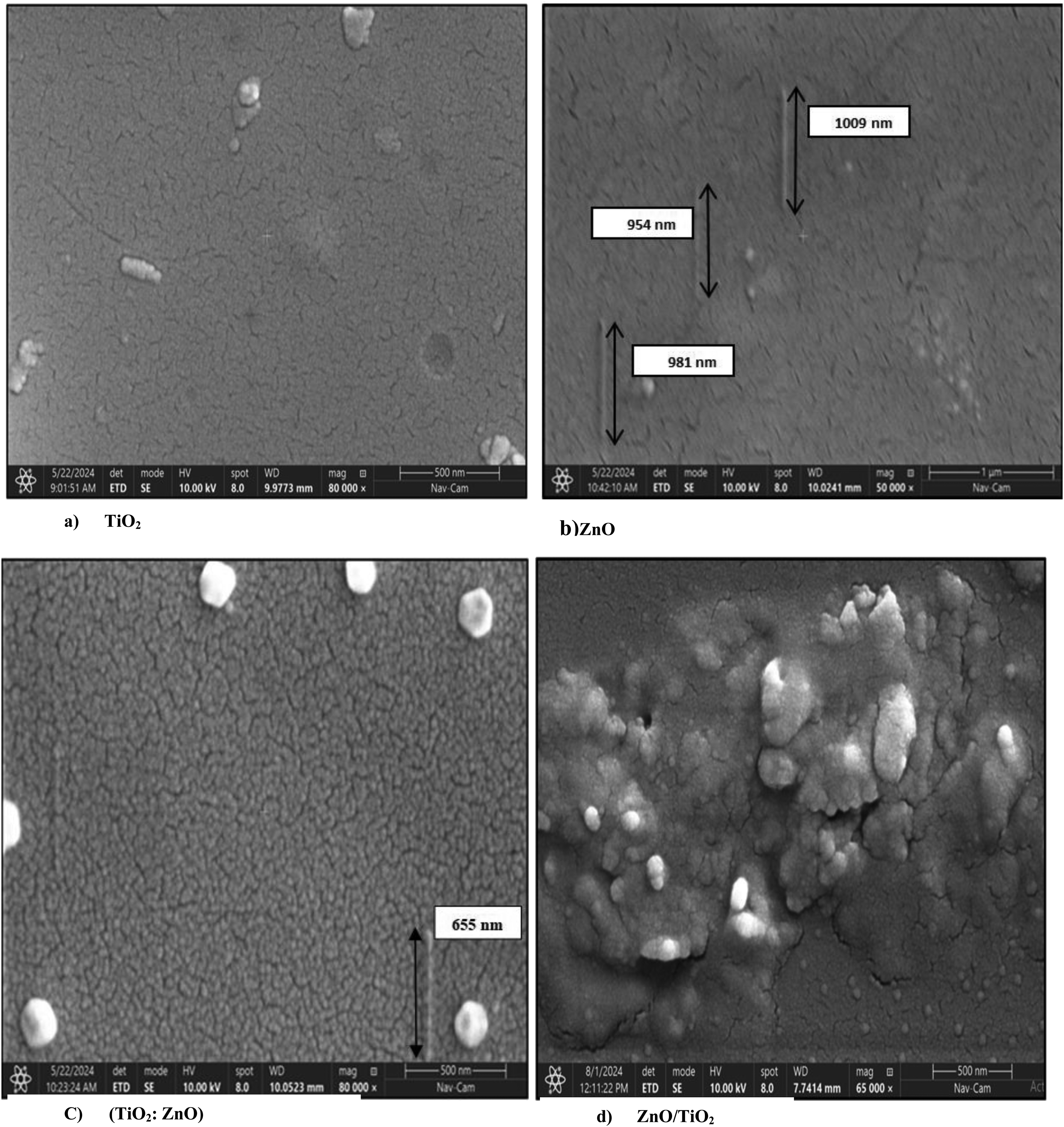
SEM images of thin films.
EDS analysis
The chemical compositions of the TiO2, ZnO, TiO2: ZnO composite, and ZnO/TiO2 bilayer thin films are determined through EDS spectra, as illustrated in Figure 6. As anticipated, the spectra reveal the presence of Ti, Zn, and O elements. Their atomic and weight contents in the thin films have been calculated based on library standards and are listed in the table attached to each figure. It is observed that the oxygen content in the film slightly decreases as with the formation of TiO2:ZnO composite and ZnO/TiO2 bilayer compared to TiO2 and ZnO. However, the measured oxygen content exceeds theoretical values, which is expected due to the nature of EDS analysis conducted via SEM, which cannot enable reliable quantification of light elements such as oxygen and carbon, etc.
Typical EDS spectra of TiO2, ZnO, TiO2: ZnO composite, and ZnO/TiO2 bilayer thin films.
Optical transmittance
Figure 7. Shows the optical transmittance spectra of the TiO2, ZnO, TiO2:ZnO composite, and ZnO/TiO2 films deposited within the wavelength range of 300–900 nm. All the films exhibit high optical transmittance, exceeding 60% in the wavelength ranges from (400-800 nm).
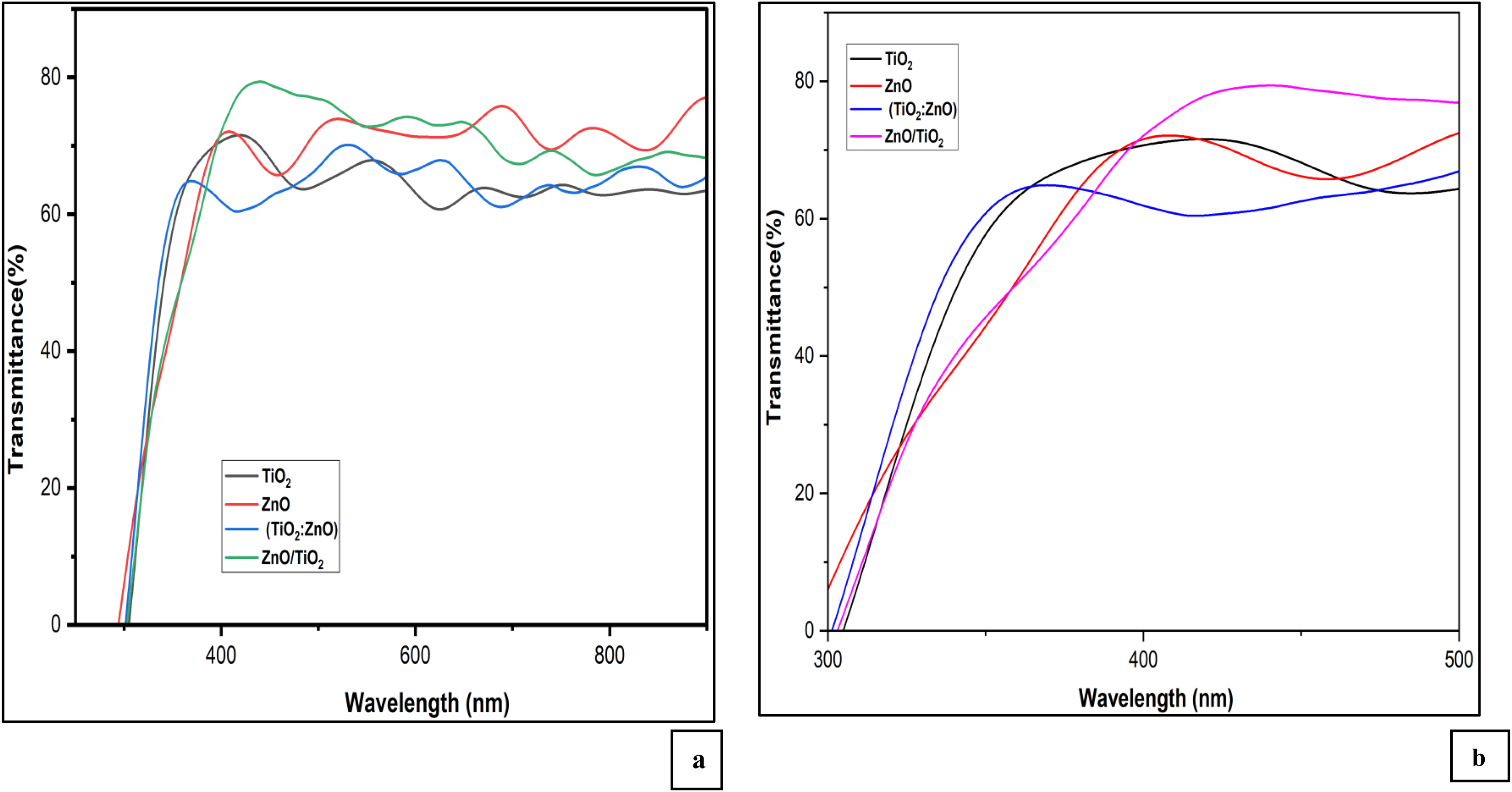
(a) Transmittance spectra of the films of TiO2, ZnO, TiO2:ZnO composite, and ZnO/TiO2,
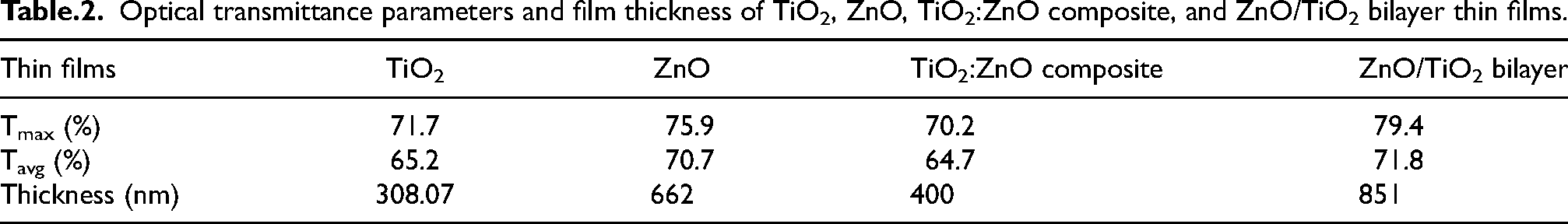
The transmittance spectra of the thin films reveal notable differences based on composition. In contrast, to provide a quantitative comparison, both the maximum transmittance (Tmax) and the average visible transmittance (Tavg) were calculated and are summarized in Table 2. The TiO2 film exhibits Tmax = 71.7% and Tavg = 65.2%, whereas the ZnO film shows improved transparency with Tmax = 75.9% and Tavg = 70.7% the higher visible transparency of ZnO is consistent with previous reports attributing this behavior to its wide direct band gap and relatively low absorption coefficient in the visible region. 38 The TiO2:ZnO composite film presents intermediate optical behavior (Tmax = 70.2%, Tavg = 64.7%), with a noticeable reduction near the absorption edge (∼395 nm) compared to the pure TiO2 and ZnO films behavior indicates the presence of defect-related localized states and possible band tailing effects, which are commonly associated with structural disorder in oxide thin films. This optical response suggests that the composite film possesses a disordered or weakly crystalline structure. This interpretation is supported by the XRD analysis, where no distinct Bragg reflections were observed within the scanned 2θ range. The absence of sharp diffraction peaks indicates that the TiO2:ZnO composite film is amorphous or poorly crystalline within the detection limits of the measurement. Therefore, the UV–Vis and XRD results are consistent, confirming that the structural disorder in the composite film significantly influences its optical behavior. Notably, the ZnO/TiO2 bilayer demonstrates the highest transparency, with Tmax = 79.4% and Tavg = 71.8%, indicating enhanced optical performance compared to the single-layer films. 39 Considering both the film morphology. From the AFM analysis, the bilayer surface consists of compact grains with a relatively intermediate RMS roughness (∼2.78 nm), which indicates a dense and fairly smooth surface. Such morphology reduces surface-induced light scattering and minimizes optical losses, thereby supporting higher measured transmittance. 40 The short wavelength portion of Figure 7(a) is expanded and shown in Figure 7(b).
Optical transmittance parameters and film thickness of TiO2, ZnO, TiO2:ZnO composite, and ZnO/TiO2 bilayer thin films.
The thickness (d) of the transparent thin films was estimated using the Swanepoel envelope method. The maximum (Tmax) and minimum (Tmin) transmittance values were extracted from the optical transmittance spectra Figure 7(a). Based on these parameters, the film thickness was calculated using the corresponding Swanepoel relation.
41

Where, n1 and n2 are the refractive indices at two adjacent maxima (or minima) corresponding to the wavelengths λ1 and λ2.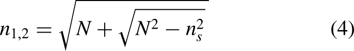
Where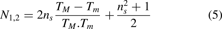
TM and Tm are maximum and minimum transmission respectively, on the envelope at a certain λ, and refractive index ns = 1.44, of the substrate. The envelopes connecting the interference maxima and minima are considered to be continuous functions of the wavelength λ.
The optical energy gap Egcan be estimated from the absorption spectrum (αhν) n, for both direct and indirect band gap semiconductors.For an indirect band gap, the optical energy gap can be estimated using the following relation2,40:
For a direct band gap, the optical energy gap can be estimated using the following relation:
Here, hν is the photon energy. The absorption coefficient α can be calculated from the transmittance T, A is a constantby the equation:
The optical band gap values for thin film were measured using the linear extrapolating method, as shown in Figure 8. From these plots, for anatase TiO2 thin films, which are typically characterized as indirect band gap semiconductors, the band gap was determined from the (αhν)1/2 versus hν plot. The indirect band gap was determined to be 3.70 eV. A similar result was reported by

Tauc plot of thin films.
For the ZnO thin films, which are known to exhibit a direct band gap nature, the band gap was extracted from the linear region of the(αhν)2 versus hν plot. The direct optical band gap was found to be 4.13 eV, which aligns with previously published values for ZnO films in the literature, typically ranging between 3.3 and 4.2 eV depending on structural quality and synthesis method,
For the TiO2:ZnO composite and ZnO/TiO2 bilayer films, both direct and indirect band gap were analyzed due of TiO2 and ZnO phases and possible interfacial electronic coupling effects. The TiO2:ZnO composite exhibited a direct band gap of 4.01 eV and an indirect band gap of 3.61 eV. The reduction in both band gap values compared to the individual oxides may be attributed to the formation of defect states, oxygen vacancies, and a possible charge transfer between Ti + 4 and Zn + 2, which introduces sub-band gap states that facilitate visible light absorption.
43
The incorporation of Zn into the TiO2 lattice also leads to lattice distortion and electronic interactions that modify the band structure,
Conclusion
TiO2, ZnO, (TiO2: ZnO composite) single layer and bilayer of ZnO/TiO2 thin films have been deposited by using a low-cost sol–gel spin coating method. After deposition, all the films were annealed at 500 °C. XRD and Raman analysis confirmed both the TiO2 and ZnO particles present in the films. In terms of morphological properties, SEM analysis revealed notable surface morphology differences among the TiO2, ZnO, TiO2:ZnO composite, and ZnO/TiO2 thin films. TiO2 showed a relatively smooth surface with minor imperfections, while ZnO elongated surface features correspond to coalesced grains or preferentially oriented growth structures. The TiO2:ZnO composite and ZnO/TiO2 bilayer thin films displayed more defined particle distributions and surface roughness, reflecting the influence of composition and processing conditions on the films’ microstructure. AFM showed the nanoparticles with average sizes of TiO2, ZnO, TiO2: ZnO composite single layer and bilayer of ZnO/TiO2 thin films are 2.7, 6.07, 0.91, and 2.78 nm respectively.FTIR analysis confirmed the presence of characteristic Ti–O–Ti and Zn–O bonds in the single and bilayer thin films. Absorption bands related to metal-oxygen vibrations, and organic residues were identified, indicating the successful formation of metal oxide structures and residual organics from the sol-gel process. The optical transmittance and band gap analyses revealed that all films exhibited high transparency. The TiO2:ZnO composite thin films and ZnO/TiO2bilayer thin films demonstrated improved optical properties and reduced band gaps, highlighting synergistic interactions and enhanced performance at the heterojunction interface.
Footnotes
Acknowledgments
The authors acknowledge the support of the Directorate-General for Scientific Research and Technological Development (DGRSDT), Ministry of Higher Education and Scientific Research of Algeria.
Ethical considerations
Not applicable.
Consent to participate
Not applicable.
Consent for publication
Not applicable.
Author contributions
Funding
The authors received no financial support for the research, authorship, and/or publication of this article.
Declaration of conflicting interests
The authors declared no potential conflicts of interest with respect to the research, authorship, and/or publication of this article.
Data availability
The data presented in this study are available from the corresponding authors upon reasonable request.