



Abstract
Reconfigurable caches offer an intriguing opportunity to tailor cache behavior to applications for better run-times and energy consumptions. While one may adapt structural cache parameters such as cache and block sizes, we adapt the memory-address-to-cache-index mapping function to the needs of an application. Using a LEON3 embedded multi-core processor with reconfigurable cache mappings, a metaheuristic search procedure, and MiBench applications, we show in this work how to accurately compare non-deterministic performances of applications and how to use this information to implement an optimization procedure that evolves application-specific cache mappings for the LEON3 multi-core processor.
Introduction
One of the major challenges processor architects have to face is the so-called memory bottleneck: the disparity in the frequencies of memory requests of processing units and latencies of DRAMs. To mask the memory access delays, multi-layered cache hierarchies have been introduced in the 70s [4], mimicking a high-speed and large main memory while using slow and inexpensive DRAM chips. This principle has been used successfully for many decades before running into performance issues in the last years. For instance, processing large data structures fills caches with data lacking temporal locality, deteriorating performances of other tasks executed on the same processor [11]. Varying memory access pattern types of applications executed by many-core systems interfere with each other, making it much more difficult for the cache to implement a coherent memory model efficiently. The consequence of these effects is that the processor manufacturers have introduced reconfigurability to caches to adapt the cache behavior to the requirements of applications [12].
Reconfigurable caches have only recently found their way into off-the-shelf processors [11]. Research in this area has started earlier, with the rise of reconfigurable logic in the 90s. The primary motivation for reconfigurable caches is that while well-configured caches with fixed architecture perform well for a broad range of applications, it is sometimes desirable to change the configuration of the cache to handle applications with atypical memory access patterns more energy-efficiently or to tailor a cache to specific use cases such as numerical simulation.
The research on reconfigurable caches subdivides roughly into structurally reconfigurable caches and application-specific memory-to-cache-index mapping functions. The work on structural cache reconfiguration investigates the benefits of dynamically changing the geometry of the cache memories, i.e., the cache’s size, the number of ways, and the number of cache blocks. Work on reconfigurable memory-address-to-cache index functions has the goal of distributing accesses to cache memories more evenly for a reduced number of conflict misses. Usually, permutation- and single-level XOR-based functions, as well as prime-moduli and multi-stage mappings, are used in related work [15].
While reconfigurability helps caches to improve their performance, trade-offs such as larger logic areas, longer hit times, and a bigger overall number of memory cells may arise. The memory overhead is, to some extent, bearable since today, most processor designs are not restricted by silicon area but by performance and performance per energy. The increase in hit time is more critical. For any embedded processors with clock frequencies well below one GHz, the pressure on the timing is moderate. On the other hand, high-performance processors have several cache levels where only the first level is optimized for hit time. Here, the reconfigurability can be applied to higher-level caches more easily.
In this work, we present an FPGA-based implementation of a processor that can freely configure its memory-to-cache-index mapping functions. We show the challenge and the solution of how to reliably compare performances of non-deterministic applications and present an implementation of an optimization procedure that can evolve application-specific cache mappings.
Related work
A conventional cache consists of one or multiple separate memories, called ways, that are usually word addressable.
onto the memory bus. The first level cache checks, whether it stores the requested data in one of its ways by splitting the memory address into the block offset
block or set index
and a tag
If one of the cache blocks in the set selected by the block index bits
In a non-conventional cache mapping scheme, the tag and index bits are transformed by two functions,
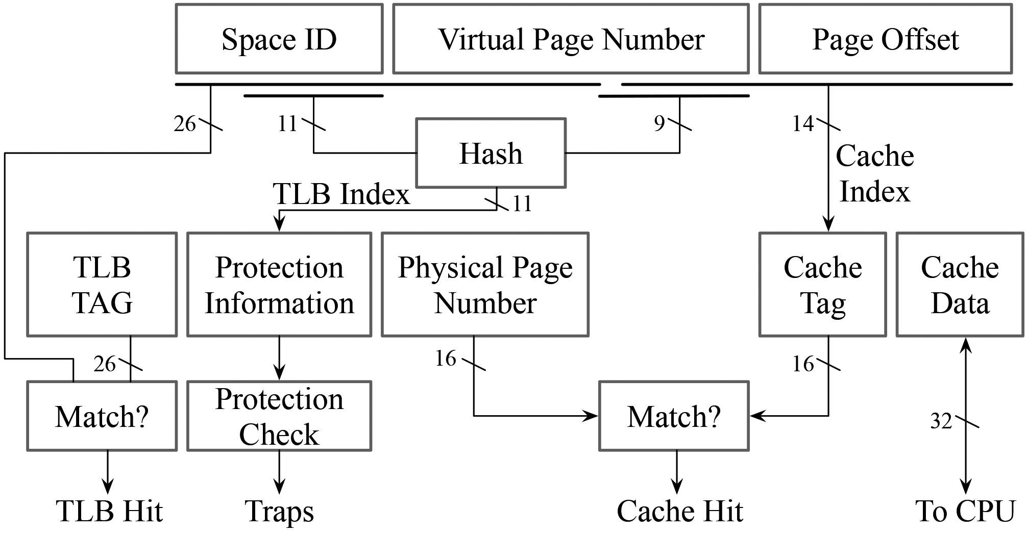
To distribute accesses to cache lines more evenly, bit address shuffling can be combined with an additional translation function. Already in the 1970s, the first mainframes with virtual memories, such as the IBM 360 and the Amdahl 470, have incorporated XOR-based mappings in their Lookaside Buffers (TLB) [19, 4]. It helped to avoid congestion as identical virtual address spaces have been assigned to all executed applications by the OS. The Amdahl mainframes, for instance, randomized the memory-to-TLB-index mapping by XOR-ing the reversed application ID bits with the virtual page number bits (c.f. Fig. 1).
The idea of hashing TLB index bits has been adopted by Vandierendonck and De Bosschere to caches [21, 22]. The authors have introduced a heuristic and an optimal algorithm for determining the input bits to the XOR planes computing the cache index depending on the memory access stream of a specific application. The authors have employed an SA-110 ARM processor model configured with a 4 KB L1 direct-mapped cache and benchmarks from the PowerStone, MediaBench, and MiBench suites. The presented cross profiling results are particularly interesting. These demonstrate the generalization behavior of the XOR mapping functions trained on a specific application and input data for different test input data sets. Two metrics are reported, the reduction of the miss rate and the reduction of the overall run time. While in nearly all cases, the miss rates were reduced over a modulo cache, the corresponding run times do not strictly follow this trend, and, occasionally, slowdowns were observed. In more recent work, Wang et al. extended this approach to the caches of a GPU in [24].
The function
Another way of defining the memory-to-cache-index function is to use a different modulus. Diamond et al. [5] investigated prime and non-prime moduli to minimize bank conflicts of a GPU. Kim et al. [15] compared XOR-based permutation, polynomial modulus, prime modulus, and own indexing schemes for various GPGPU workloads. They were able to reduce computation time and energy consumption significantly.
Our approach can be seen as an methodological extension of the work of Vandierendonck et al. [23]. Similarly to Vandierendonck et al., we introduce a mapping function consisting of Boolean gates between the processor and the cache memories. However, we do not restrict the translation complexity to one level of XOR gates. Instead, the cache translation function is defined as a multi-level circuit composed of 2-input Look-up Tables (LUT). The LUT’s are embedded into a butterfly network, and their content is subject to an optimization algorithm. Such translation functions can compute any Boolean circuit of a certain size [10, 9, 14] and have the potential to outperform Vandierendonck’s approach. Additionally, as LUTs content is reconfigurable at run-time, application-specific cache mappings can be realized naturally. That is, during an offline phase, a well-performing cache mapping for an application is evolved and embedded into a segment of application’s binary. Later, in the regular operation phase of the application, application’s optimized cache mapping is configured into the memory-to-cache-index translation block on, e.g., a task switch by the OS scheduler and allow the application to execute with fewer cache misses.
This work is organized as follows. Section 3 presents the LEON3 processor implementation with reconfigurable cache address translation functions. The optimization method and the performance assessment procedure are presented in Secections 4 and 5. Secection 6 shows how the optimization algorithm has been configured, and Secection 7 presents the results of this paper. Finally, Secection 8 summarizes the insights and concludes this work.
Relevant components of a LEON3 core and our extensions to the LEON3 architecture, colored in grey. The instruction cache is indexed using virtual and the data cache using physical addresses.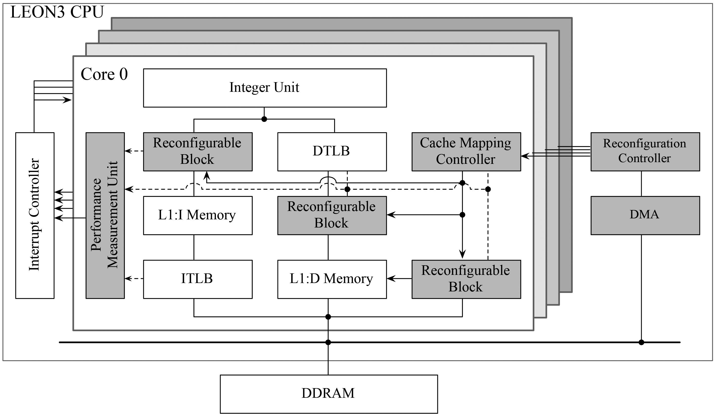
a. The butterfly network of an RCB with 4 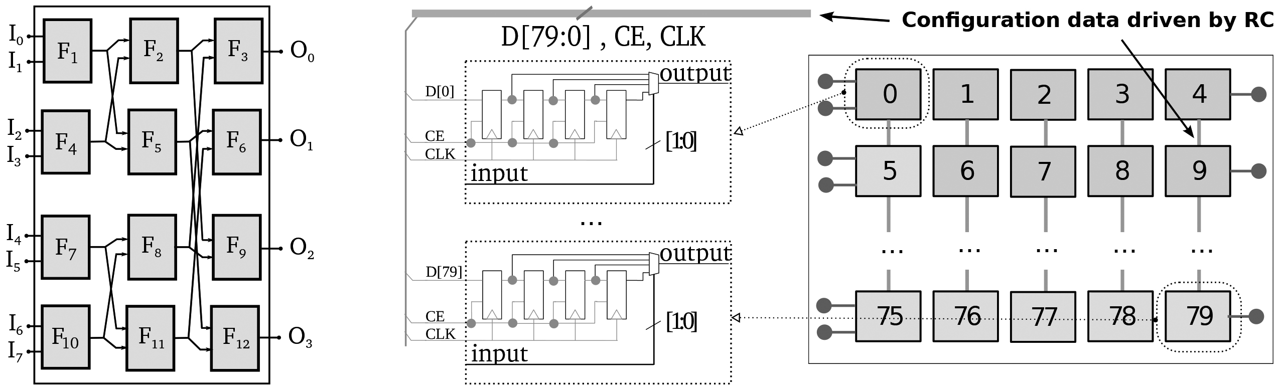
For this work, we are using the embedded open-source LEON3 processor with one level of private instruction and data caches per core [1]. An open-source L2 cache implementation was not available for LEON3 at the starting time of our work.
The reconfigurable cache mapping architecture consists of Cache Mapping Controllers (CMC), the Reconfiguration Controller (RC), and the Reconfigurable Blocks (RCB) (c.f. Fig. 2). The task of the CMCs that are located in each core is to relay reconfiguration requests from the cores to the RC and to manage RCBs’ cache mapping reconfiguration process. The RC gets and serializes reconfiguration requests from CMCs and uses DMA to fetch reconfiguration bitstreams for the RCBs efficiently. The RCBs implement the reconfigurable cache mapping functions. Each core has a set of three active RCBs (L1:I, L1:D, and the snooping mechanism of L1:D) and at least one set of shadow RCBs for masking the reconfiguration time. LEON3’s L1:I caches do not implement a coherent memory model and need no synchronization of modified cache blocks among the cores.
An RCB implements a 16
The reconfiguration of cache mappings is done through a Linux driver. The driver allows userspace programs to load and read cache mapping configuration bitstreams and test their functionality. During the power-up of the LEON3 cores, all RCBs are initialized with the conventional modulo mapping to mimic the standard behavior of a cache. The applications’ performance when using custom cache mappings is metered through the Linux’ perf_tool command [8].
The implementation overheads for the presented modules are shown in the left part of Table 1. The baseline configuration is a LEON3 4-core processor synthesized with direct-mapped 4KB instruction and data caches. The implementation consumes 13 Distributed RAMs (DRAMs), where RAM32x1D primitives are used. There is an overhead for the implementation of cache memories/-controllers, as the comparators for hit/miss detection are wider. In the original LEON3 cache implementation, not all bits of Block RAMs (BRAM), which are used to store cache tags and blocks, are employed. This results in steady BRAM usage.
Hardware resources used by a LEON3 core and the parameters of the LEON3 platform implementing reconfigurable cache mappings
The right part of Table 1 summarizes the parameters of the prototype system. The prototype is implemented on a Xilinx ML605 board equipped with a Virtex-6 FPGA. The reconfigurable circuits are implemented for L1:I and L1:D caches.
To find well-performing cache mappings, we rely on a heuristic search method. The three main components of a heuristic are (a) a formal representation of a candidate solution, i.e., the encoding model, (b) functions that are able to combine and modify candidate solutions, i.e., variation operators, and (c) a metric that assesses the performance of a candidate solution, i.e., the objective function. This section presents the encoding model, the variation operators, and the heuristic procedure. The subsequent section shows how the performance of an application can be reliably assessed.
The encoding model for the bitstream of an RCB
Cartesian Genetic Program (top), its encoding (bottom), and the set of nodes’ functions (right).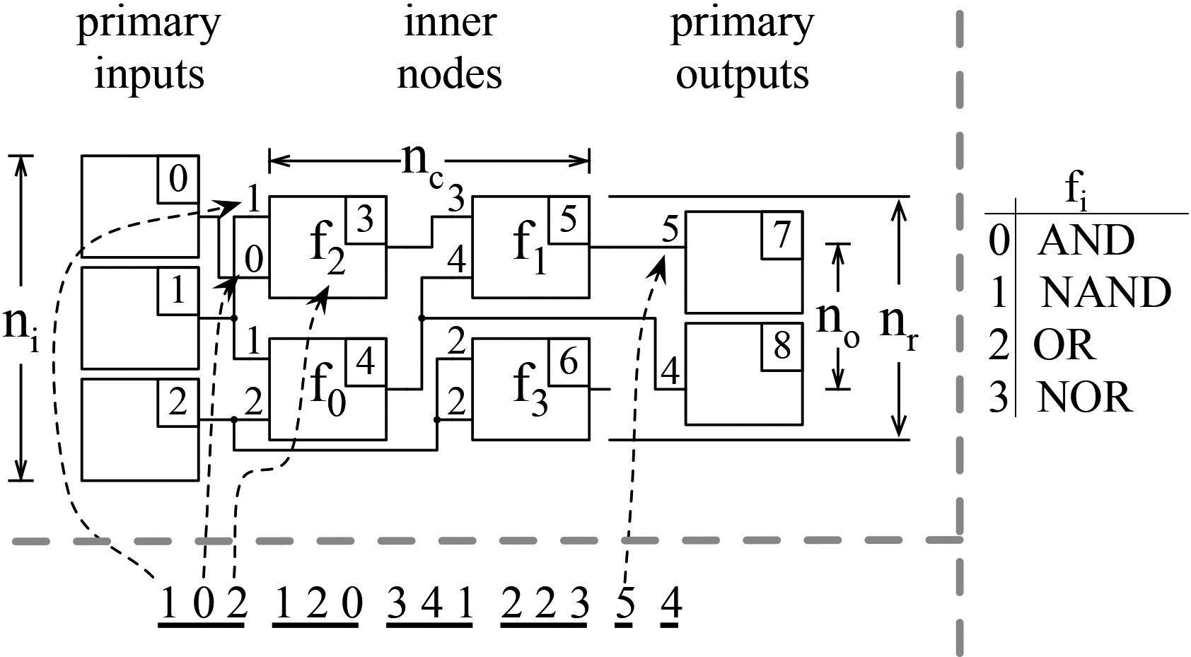
To encode a function consisting of a two-dimensional grid of reconfigurable LUTs that maps memory addresses to cache indexes, we employ the Cartesian Genetic Programming (CGP) model [13]. CGP is an evolutionary optimization technique and was invented to capture FPGA circuits. It encodes a circuit as a directed acyclic graph (DAG). An exemplification of the encoding is illustrated in Fig. 4. The graph nodes are arranged as a
The graph in CGP is encoded by a linear list of integers, which is called a genotype and shown at the bottom of Fig. 4. The first
We adopt CGP for the encoding of the configuration of an RCB (c.f. Fig. 3b) by setting the configuration of connection genes such that the resulting wires define a butterfly network. The connection genes are then fixed and are not subject to the optimization algorithm. The encoding of the function genes of
CGP’s variation operator is called mutation. Given the mutation rate and the size of the genotype, the operator computes how many genes have to be mutated. These genes are then selected randomly. A function gene is mutated by choosing a random function descriptor. A connection gene is mutated by randomly rewiring it to a preceding node within the range given by the levels back parameter.
We adopt CGP’s mutation operator by letting it mutate only the function genes. More precisely, given a mutation rate of, e.g., 1%,
(
Termination condition not met
The optimization algorithm
CGP is traditionally optimized by an (
The challenge of an accurate performance estimation
The distributions of Misses Per 1000 Instructions (MPKI) measured for the conventional (left column) and two randomly sampled cache mappings (center and right columns). The L1:D cache is configured as a 4 kB directly-associative and physically-addressed cache. The experiments are conducted for the CJPEG application and four different input images (vectors 0 …3).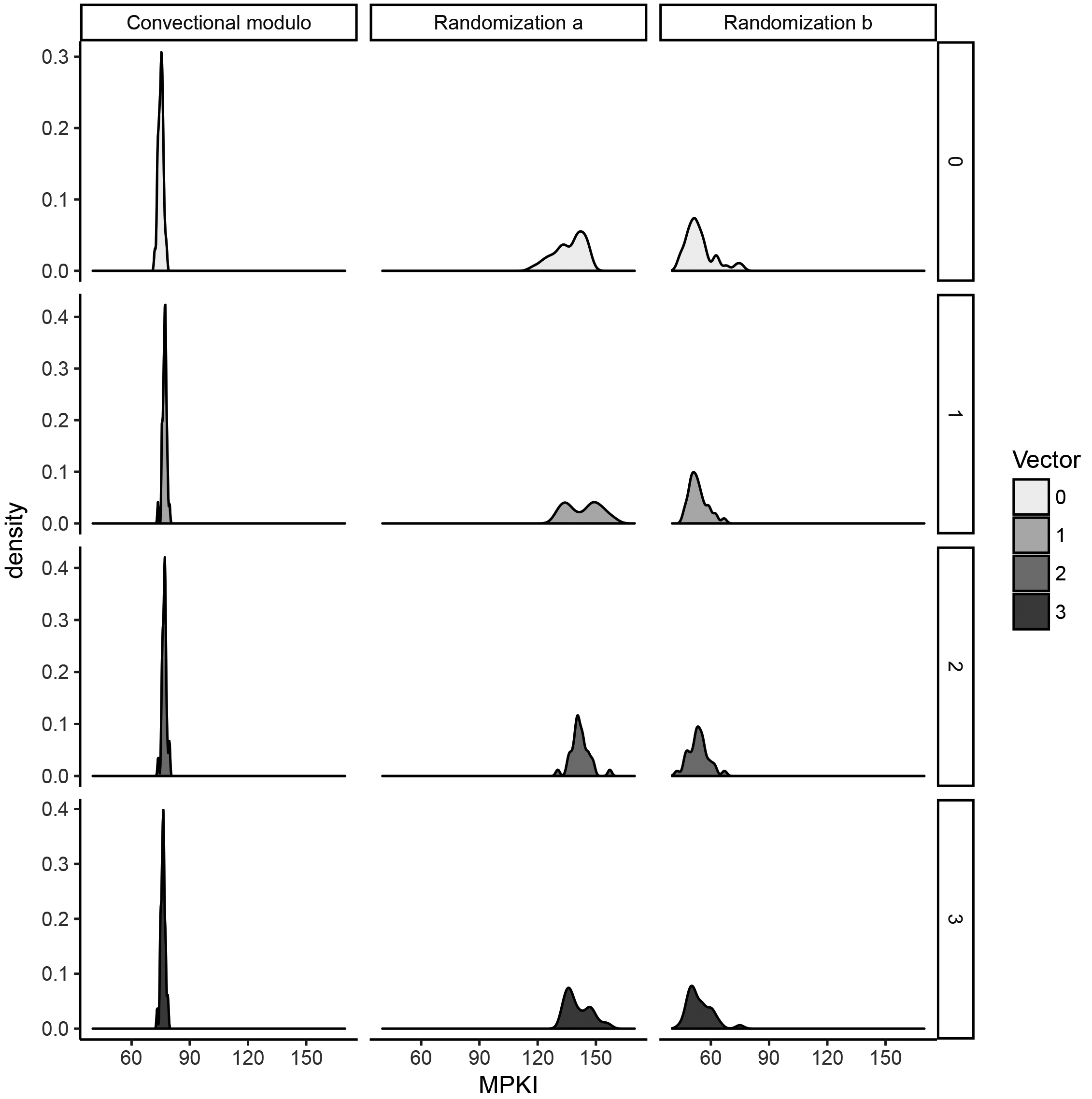
When metering a deterministic application, the general assumption is usually that the experiment will produce either deterministic measurements or measurements with negligible deviations. This assumption often holds for many of the related works that are using software simulators for system analysis. In our case, however, execution of an application on a multi-core system in an environment where concurrent applications are competing for the resources such as disk IO, cache space, processing time, and network bandwidth results in measurement variations that make comparing different computing architectures difficult. An example is given in Fig. 5, where sub-plots are showing histograms for L1:D miss-rate measurement variations of the CJPEG executable employing three different cache mapping functions and applied on four different images. The
where
The numbers in Fig. 5 have been conducted in experiments where we have pinpointed CJPEG to a dedicated core and minimized the execution of concurrent applications (context switches) to a single-digit rate. Despite all measures, and this is the first observation, MPKI deviations for the original and unchanged LEON3 processor executing a JPEG benchmark haven’t vanished completely, as can be observed in the left column of Fig. 5. The variation magnitude corresponds to the number of evicted cache blocks by concurrent applications and Linux kernel service functions. As these interference sources can hardly be eliminated on a multi-tasking system, we assume that this is the most accurate MPKI measurement precision that can be achieved on our system on average.
The deviation magnitude of MPKI measurements increases for the two randomly generated cache mappings (middle and right-hand column in Fig. 5). The mechanism behind this observation originates in Linux’s virtual-to-physical page mapping randomization. To prevent malicious software from reliably guessing physical pages with sensitive application data, virtual pages are allocated to randomly selected physical pages. If one would record the issued physical addresses of two benchmark executions, only the lower address bits indexing within a physical page would match. Higher bits would be randomized by Linux’s virtual-to-physical page mapping obfuscation mechanism. We have configured the L1:D cache to be of the same size as a physical page. This means that the conventional cache mapping operates only on non-randomized address bits, i.e., the cache mapping experiences for every benchmark execution the same sequence of input bit vectors. This is different for the randomized cache mappings, as these mappings are defined on all address bits and are experiencing for every benchmark execution addresses with varying upper bits. Consequently, cache blocks are indexed in a different order for every CJPEG execution, which results in a changing number of cache block evictions and miss rates. The middle and right columns in Fig. 5 show how Linux’ virtual-to-physical page randomization increases the variance of MPKI values compared to baseline MPKI distributions (left column in Fig. 5). Given these observations, the conclusion is that the typical performance of a cache mapping needs to be derived from a set of measurements.
To compare populations of measurements, one usually resorts to statistical methods. The very first question is whether the samples of a population are normally distributed. This leads us to the second observation: The histograms in the central and left columns of Fig. 5 already suggest that MPKI values of some cache mappings do not follow the normal distribution. To verify this, we have tested during an optimization run the MPKI distributions generated by 7508 cache functions using the Shapiro-Wilk, Kolmogorov-Smirnov, and Anderson-Darling tests at the confidence level of
The third observation is that MPKI distributions are not only not-normal but also different. The central and right columns in Fig. 5 are showing that histogram shapes are dissimilar and have differently distributed peaks. This is a frequent finding throughout our experiments. When distributions are different, non-parametric tests comparing the central tendencies while relying on the prerequisite of identical distributions cannot be used anymore (
The search for good performing cache mapping functions has to ensure that candidate solutions excel for a wide range of potential input vectors for some application
Recording
As motivated previously, we have selected the Wilcoxon rank-sum test to compare cache mappings. When comparing the sample populations
Under the null hypothesis
The run-time of an optimization algorithm is typically dominated by the complexity of the performance assessment of a candidate solution. The cache mapping’s performance is defined in our work as a set
During the initial experiments, we observed that most of the off-spring individuals had a lower performance as their parent. We use this observation to minimize the number of candidate solution executions
Statistical Wilcoxon rank-sum test: The upper triangular parts show CDF for all pair comparisons of a (1 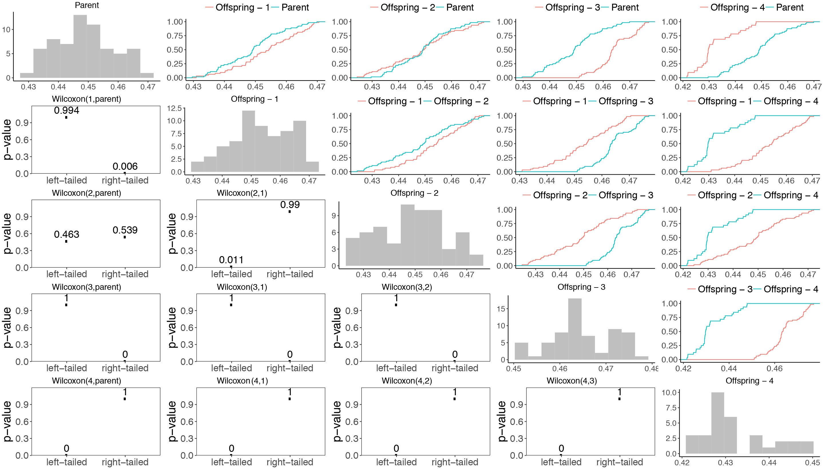
For, e.g., a (1 Off-spring individuals are removed if the test rejects the null-hypothesis for them. The remaining individuals are executed again on four input vectors 16 times and the resulting sets If at least one off-spring candidate remains after the first phase, children and the parent are joined into a common set
To illustrate the procedure, we have collected sample data from one generation of a CJPEG optimization run. Figure 6 shows a side-by-side comparison of CDFs for all 2-tuples (parent and four children) in the upper-right triangle, the distribution of
Breakdown of the distribution of the cumulated number of CJPEG executions on four input vectors before a sufficient amount of data is collected for the rank-sum test to make a decision.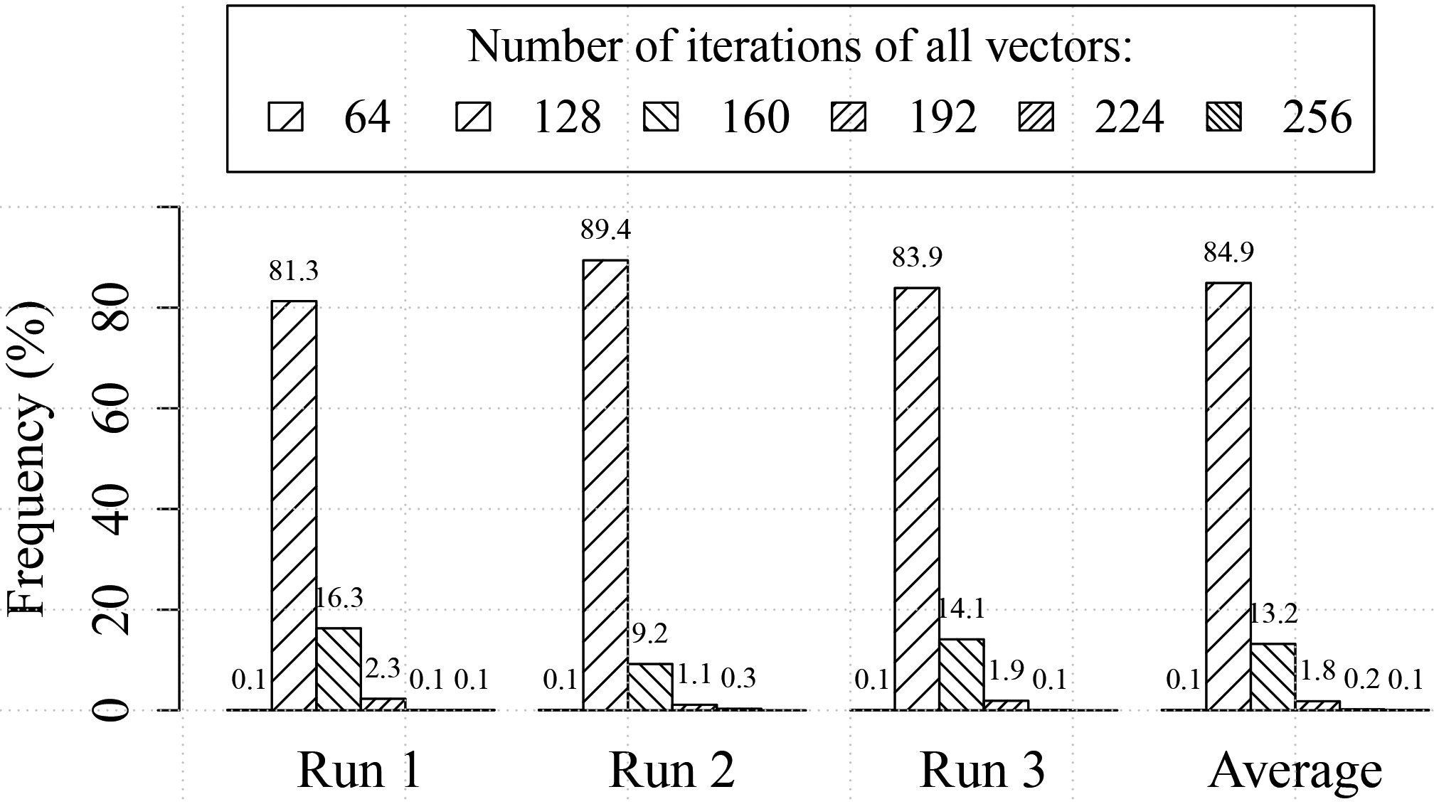
Figure 7 shows the potential of the “early-stop” strategy. It plots the average number of CJPEG executions required to make a comparison. The data is collected in three CJPEG (1
The main parameters responsible for the convergence rate of the
Configuring the
evolutionary algorithm
(1 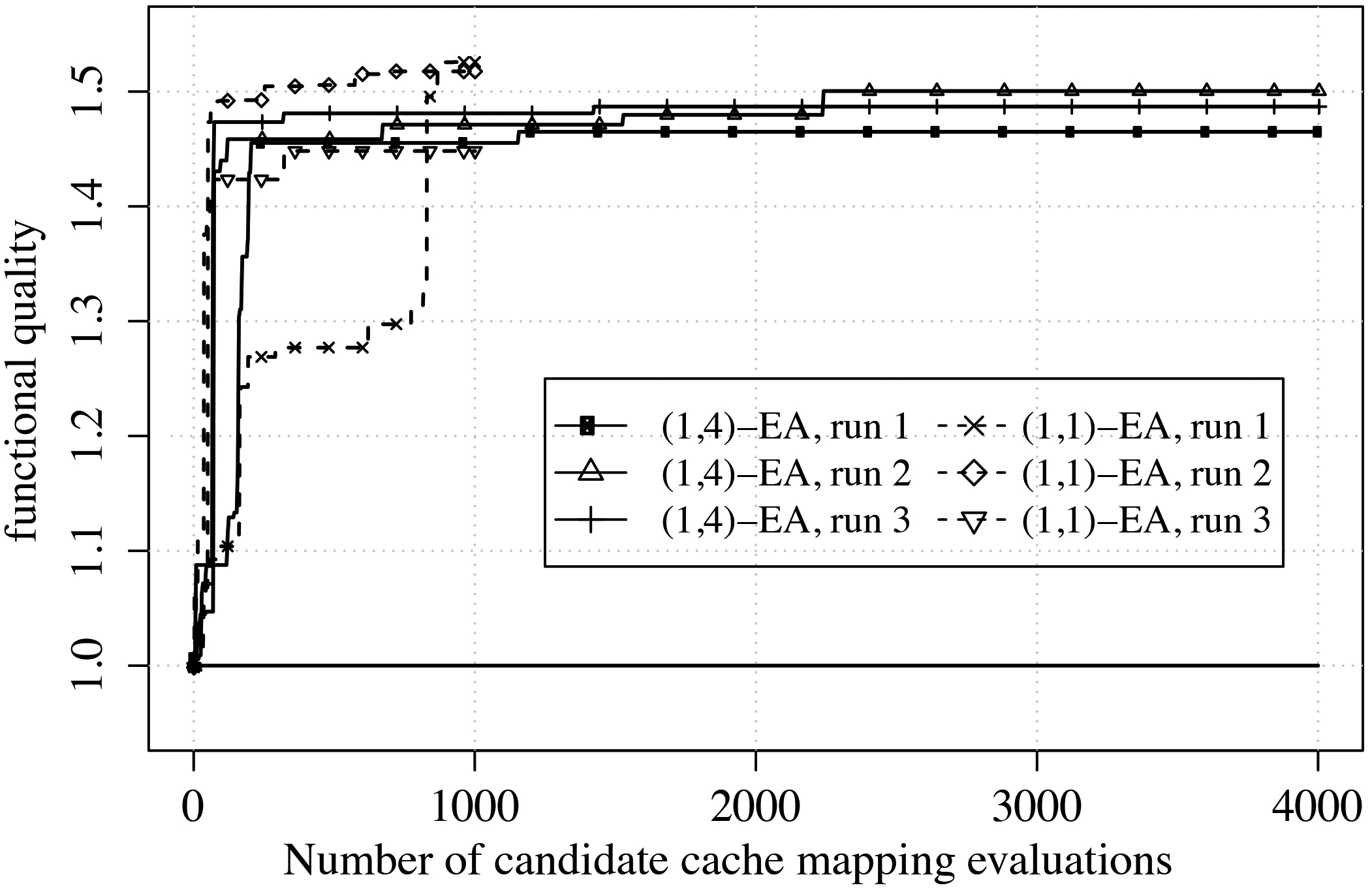
We tested the EA using different values for
Amount of mutated genetic material that led to improved L1:D cache mappings.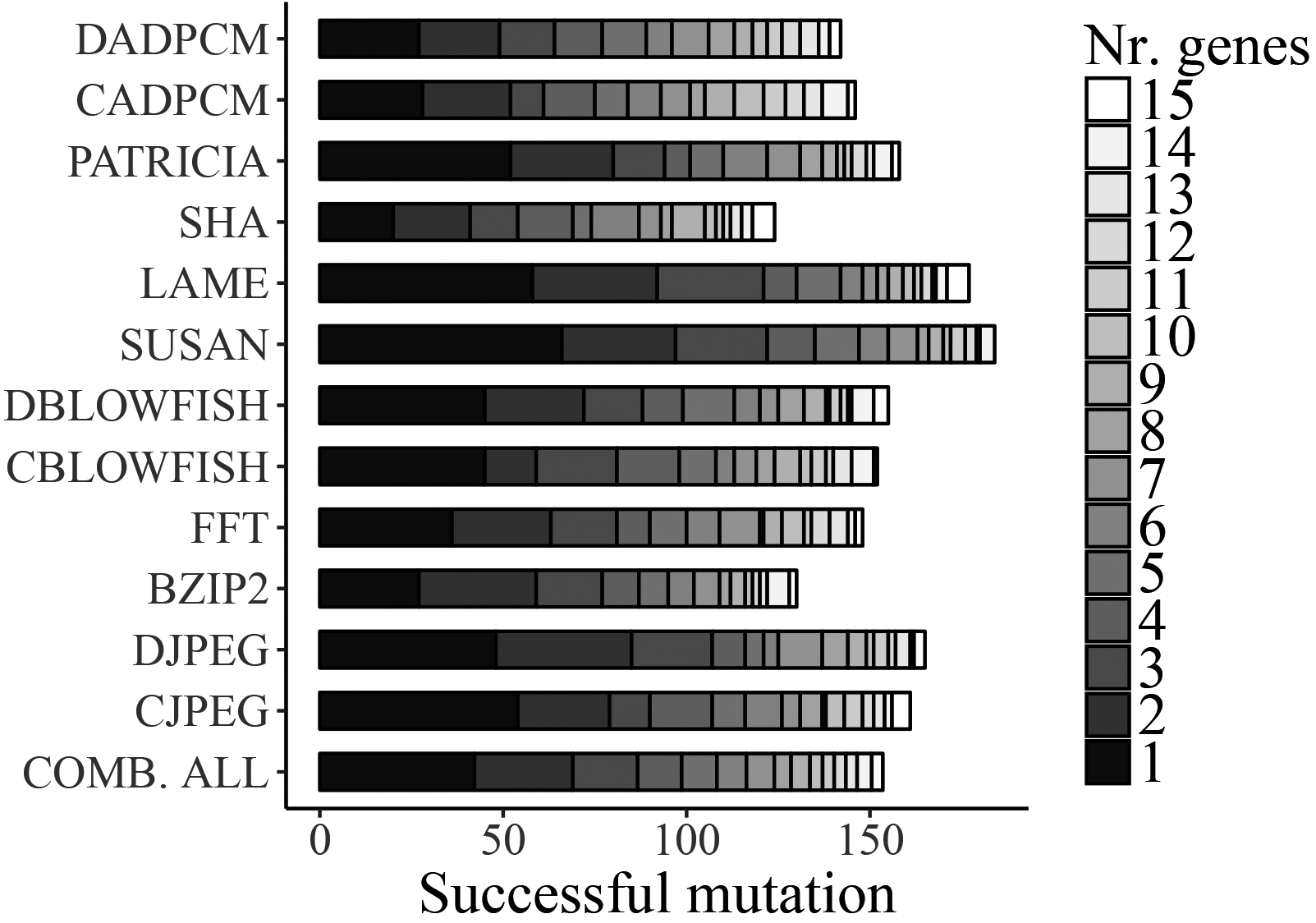
Amount of mutated genetic material that led to improved L1:I cache mappings.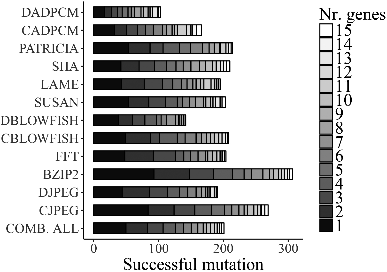
Our strategy for finding well-performing mutation rates is to let the mutation operator sample the amount of mutated genetic material each time freely between 0% and 25%. The mutation rates that created better off-spring candidates during the optimization runs were recorded.
Figures 9 and 10 present stacked distributions for the amount of mutated genetic material for successfully improving L1:D and L1:I cache mappings. The first general observation is that mutating less genetic material is more effective than mutating a lot of genes. The second observation is that roughly half of successful mutations are the consequence of changing up to three genes. Based on these insights, we have defined gene mutation probability distributions of
Evolution of custom cache mappings for a 4 KB direct mapped cache. Normalized median training and test miss-rate reductions (red.[%]) of the best evolved cache mapping of an application. Median absolute and relative numbers of miss-rates during testing (
If an application would like to employ custom cache mappings, it has to evolve these mappings in a preparational step. Once custom mappings are evolved, no further optimization is required. Later, during the regular operation of the application, its custom cache mappings can be activated by the task scheduler on a context switch.
To simulate the lifetime of a custom cache mapping, we subdivide the experiments into two phases. In the first, the training phase, custom cache mappings are evolved and stored along with the application’s binary. The results of this phase are presented in Section 7.2. In the second, the validation phase presented in Section 7.3 the regular operation of an application is simulated. The application is executed under typical conditions, and its performance is measured using the conventional and custom cache mappings.
The experimental system
The overall experimental system consists of a host computer carrying out the EA and distributing candidate cache mapping evaluation jobs to multiple FPGA boards. When the client FPGA board receives an application, its candidate cache mapping, and application’s input data vector, the cache mapping circuits are reconfigured on all affected LEON3 cores. Then the client process fork()’s and migrates to the target cores. There, the memory image of the process is duplicated by Linux’s perf, which executes the target application with the according to input vector. Once the execution is finished, perf returns the collected metrics to the host process.
We evolve cache mappings for applications from the MiBench suite. For each application, data and instruction cache mappings are evolved in separate experiments. Three optimization runs are executed for 3000 generations for each application, and the best performing cache mapping out of these runs is selected and tested in the validation phase. During the optimization, the performances of candidate cache mappings are evaluated on four different training- and the best-evolved cache mappings on ten different validation data vectors. In the training phase, an application is executed on a single test data vector up to 12 and in the validation phase on a test data vector 16 times. The performance of a cache mapping is reported as the normalized median miss rate overall execution repetitions of an application and its cache mapping on all of its input data vectors.
Evolution of custom cache mappings for a 4 KB 2-way cache. Normalized median training and test miss-rate reductions (red.[%]) of the best evolved cache mapping of an application. Median absolute and relative numbers of miss-rates during testing (
, rate[%]). Median run-time reductions during testing
Evolution of custom cache mappings for a 4 KB 2-way cache. Normalized median training and test miss-rate reductions (red.[%]) of the best evolved cache mapping of an application. Median absolute and relative numbers of miss-rates during testing (
The training results of best-evolved cache mappings are presented in the “training red.[%]” columns for L1:D and L1:I caches in Tables 2 and 3. The first observation is that the optimization process is always able to find better cache mappings than the standard mapping for data and instruction caches. The improvements lie up to 10% for the data and usually above 10% for the instruction caches. Sometimes, the MPKI improvements are rather large. For CJPEG and RIJNDAEL (L1:D, directly mapped) and DBLOWFISH as well as CRC32 (L1:D, direct-mapped and 2-way associative) the improvements are above 30%. For DJPEG (L1:I, direct-mapped), the MPKI reduction reaches 64.5%. These numbers show the potential for the improvement of cache miss rates.
The second observation is that fetching instructions can be predicted better than fetching data memory accesses. This is even though the L1:D cache usually shows higher relative miss rates than the L1:I cache for many applications and therefore, intuitively, L1:D should have a higher potential for miss-rate improvement (column: testing
Testing custom cache mappings: The validation phase
To investigate how an application with a custom cache mapping behaves in a regular operation mode, we test the best cache mappings on the application’s input data vectors that have not been used in the previous section. We report the absolute cache miss rates (testing
The first observation is that the reduction of cache misses (testing
The next observation is that, similar to training results, the instruction cache accesses can be predicted more accurately than data cache accesses. For data caches, the MPKI improvements lie up to roughly 5% except for the CJPEG benchmark (L1:D, direct-mapped) with 35.2% MPKI improvement, while for instruction caches the improvements are often above 10%.
The final observation is that the run-times can be improved, however, not to the extent reached by MPKI reductions. This is due to the fact that either the data or the instruction cache has been optimized and tested at the same time. I.e., reducing the miss-rate of CJPEG by 35% reduces the execution time only by 16.8% (L1:D, direct-mapped). The run-time improvements for the direct-mapped cache are pronounced for the CJPEG (L1:D, 16.8%), DJPEG (L1:I, 8.7%), DIJKSTRA (L1: I, 9.7%), RIJNDAEL-DE (L1:I, 26.3%), RIJNDAEL- EN (L1:I, 18.8%), and the CRC32 (L1:I, 37.1%) applications. For the set-associative cache, the run-time improvements are, as expected, smaller and lie around the performance of the conventional cache with the exceptions for the CJPEG, RIJNDAEL-DE (L1:I, 9.7%) benchmark.
Conclusion
The trend for more cores on a single die challenges the conventional processor design. Applications with fundamentally different memory access behaviors interfere with each other making it difficult for the cache logic to provide a uniform, coherent and efficient memory model. Shared resources allow for information leaks among unprivileged tasks. The memory bottleneck and caches are becoming one of the popular research and development fields of processor design again.
In this work, we have investigated the idea that a reconfigurable memory-address-to-cache-index mapping that is tailored by a search algorithm to a specific application may outperform the conventional modulo-mapping. We have extended for the instruction and data caches of LEON3 by reconfigurable address mapping functions, interfaced them with the Linux OS Kernel, adopted Linux’ scheduler, and evolved for nine applications for the L1:I and L1:D application-specific cache mappings. For most of the applications, the L1:I miss rates could be improved by more than 10%. Most of the execution times for L1:I and L1:D lie, however, around the performance of systems with a conventional cache. Large run-time improvements have been achieved for the Rijndael-DE (26.3%), Rijndael-EN (18.8%), CRC32 (37.1%), and CJPEG (16.8%) benchmarks.