
Abstract
Power amplifier is a crucial part of the active magnetic bearing system, and its precision characteristic is decisive to the overall systematic performance. The bi-state and tri-state modulations are both widely used in the design of DSPA, and generally there are many approaches to realize the design. DSPA will have different output performance under different modulations. In this paper, we propose a unified design of digital switching power amplifier (DSPA), which can be compatible with different modulations by configuration of hardware only. As many factors will influence the current ripple characteristic of DSPA, an approach based on Fourier series has been proposed to establish the equivalent mathematical model of DSPA under both bi-state and the tri-state modulations. We analyze the approximated theoretical ripple characteristic of DSPA with the unified architecture design discussed, and provide the simulation based on the equivalent mathematical model, then establish the experimental platform to verify the analysis of current ripple characteristic under different conditions. Experimental results show that the ripple characteristic has been influenced mainly by bus voltage, modulation frequency and time constant of load, and the approach proposed in this paper can effectively describe the ripple characteristic of DSPA under different modulations.
Keywords
Nomenclature
Introduction
With the advantages of no mechanical contact, no wear, no lubrication and controllable bearing characteristics, magnetic-levitated actuators are the crucial components of the equipment, such as turbine machine, vacuum pump, high-end manufacturing facilities and attitude control gyroscope of spacecraft [1, 2]. MLPAs (magnetically levitated planar actuators) are the common forms [1, 3, 4] for planar motion, widely used in 6 degrees-of-freedom (DOF) ultra-precision stage [5, 6]; while the magnetic bearings are the other common forms for rotational motion application. Power amplifier (PA) in magnetic bearing system can be regarded as the current tracking control system, which provides the desired current in the electromagnetic coil of the active magnetic-levitated bearings. The performance of the power amplifier affects the stability and dynamic characteristics of the whole system [2, 7].
The current ripple is one of the crucial performance indicators of the PA in the active magnetic-levitated bearings. The excessive ripple will increase the additional copper loss and the eddy current loss [4, 8]. And also, the nonlinear control region of controlled current will be increased [1, 9], leading to the mechanical vibration of the rotor intensified. Furthermore, the intense vibration of the rotor may lead to instability of high speed rotor. Therefore, the low output current ripple characteristics are the crucial point that must be considered in the design of the PA for active magnetic-levitated bearings.
Digital switching power amplifier (DSPA) has been more widely used. Compared with analog control, the digital control provides the ability to decrease the disturbances in the analog signals, and to operate more complex arithmetic, more robustness against aging and environment variation [10]. However, digital control results in inherent time delays simultaneously, and the too-large phase shift even endangers the system stability [10]. Some control strategies, e.g., dead beat control [11, 12], predictive control [13, 14], and repetitive control [15, 16] have been proposed to compensated the delays in digital close loop, and nearly achieve zero current error in theory [10]. However, the control strategies above are sensitive to system parameter variations, which means that the uncertainty in model will cause the uncertainty in output performance.
There are different architectures for DSPA with different modulations (bi-state or tri-state), and due to nonlinearity from switch tube and diode, or dead band, it is difficult to establish an accuracy model to analyze the performance of DSPA, therefore the existing approaches are deficient to guide the design. Zeng et al. [17] introduced the linearized electromagnetic force equations, and according those, the PA can be equivalent to proportional component. Or the DSPA had been seen as a simplified first-order system [18], however, this simplified model above can approximately describe change trend only. The state space of the nonlinear circuit [19] was established but can be used to analyze the DC steady-state characteristics. Power circuit model from the Matlab/Simulink [20, 21] can be used in simulation, but lacks clear physical concepts [22].
In this paper, we propose a unified architecture design of DSPA, compatible with both bi-state and tri-state modulations conveniently, to provide the possibilities for analyzing the performance of DSPA under different topology or modulations. By using the Fourier series [22], we establish the mathematical model and simulation of this unified design. Finally, the experimental platform had been built to verify the accuracy of the approaches in this paper.
Unified design of DSPA in magnetic-levitated bearings
Unified design of DSPA
Magnetic-levitated bearing control system includes position and current feedback close-loop control, as shown in Fig. 1. Position controller output the desired current commands according to the rotor position errors, and then the current controller realizes the output of desired load current following the command, leading to the generation of desired electromagnetic force to maintain the stability of the rotor. The generation of electromagnetic force relies on a current close-loop, which is implemented in one DSPA – its block diagram is shown in the dashed box in Fig. 1. The general active magnetic-levitated bearing system is a 5-DOF (degree of freedom) system, including 10 current close-loops as in Fig. 1, while the magnetic levitated bearing system with redundant supporting structure [8, 23] needs more DSPAs.
Block diagram of general 5-DOF magnetic-levitated bearing system.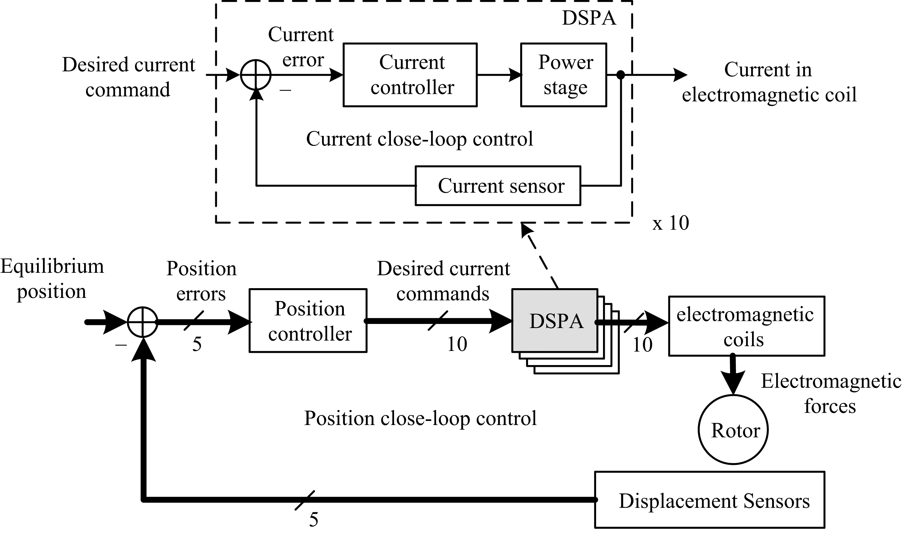
We define DSPA as 3 parts, as the upper in Fig. 2. The difference between bi-state and tri-state modulation in implementation is the phase relationship of PWM modulation signals, which means that we only need to design a unified controller suitable for both modulations and meanwhile select the same power stage and current sensor parts. Essentially DSPA is a current tracking system, relying on the close-loop feedback control to generate desired load current. As in Fig. 2, a digital controller is designed in DSP (digital signal processor) and FPGA (field programmable gate array), and the outputs of the controller are converted into modulation signals through PWM generator, to drive the power circuit. The ratio of modulation signals will affect the change of current in every PWM cycle.
Considering that it is difficult to implement different precise phase shift for a PWM signal according to different application requirement, we add a phase shifter implemented in FPGA. A PWM generator is designed to provide PWM modulation signals CT1 and CT2, with different phase relationship under bi-state and tri-state modulation, which means it only needs to configure the controller by software but not design the new hardware circuits. This style of unified design shows its good compatibility in magnetic levitated bearings system.
The unified design of DSPA.
DSPA has different current ripple performances under bi-state and tri-state modulations. The current flow under bi-state modulation is shown in Fig. 3, where,
The current flows under bi-state modulation, (a) current increasing process, (b) current deceasing process.
In bi-state modulation, CT1 and CT2 can be only enabled or disabled synchronously to turn on or off the power tubes, leading to 2 different current changing process. When CT1 and CT2 are enabled, the current in electromagnetic coil, as the dotted arrow shown in Fig. 3a, increases under the effects of bus voltage and the electromagnetic coil has been charged; while CT1 and CT2 are disabled, as shown in Fig. 3b, the current loop is established by the freewheeling diodes, D1 and D2, and the energy stored in coil feed back to the bus power with the current decreasing.
In tri-state modulation, CT1 and CT2 can be asynchronously enabled or disabled, leading to 3 different current changing process. When CT1 and CT2 are enabled or disabled synchronously as in Fig. 4a or b, the conditions are same as in Fig. 1, leading to the current increasing or decreasing processes; while enabling the CT1 and disabling the CT2, the current flow is as shown in Fig. 4c, there is no energy exchange, leading to a current remaining process. Figure 4d illustrates another current remaining process when CT1 disabled and CT2 enabled.
The current flow under tri-state modulation, (a) current increasing process, (b) current deceasing process, (c) and (d) current remaining process.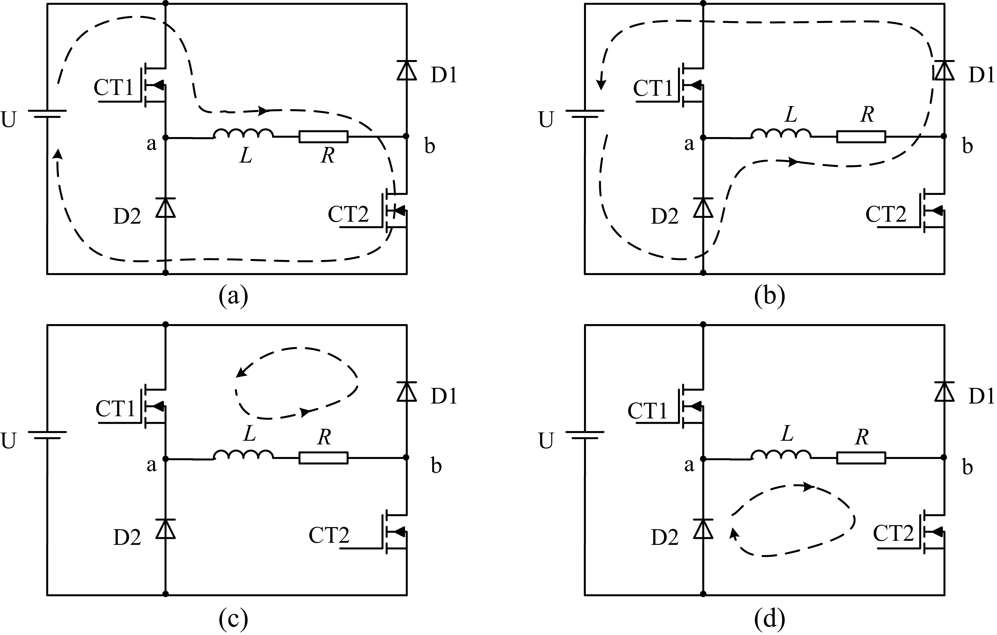
Considering that we need a unified architecture for different application, PWM generator need to provide PWM signals with different modulation frequency and phase shift, which are the key to be compatible with two modulation modes. DSP has the EPWM module, an internal peripheral, can be used to generate desired PWM signal by setting the duty value and period value.
Figure 5 illustrates the principle of PWM generator, which has been divided into 2 parts implemented in DSP and FPGA respectively. In DSP, we can set the period and duty value to generate the original PWM signals, as the upper part in Fig. 5. A phase shifter is design in FPGA to provide the relevant driving signals under both modulations, because it is difficult to shift a changeable phase by DSP only.
Realization of PWM generator.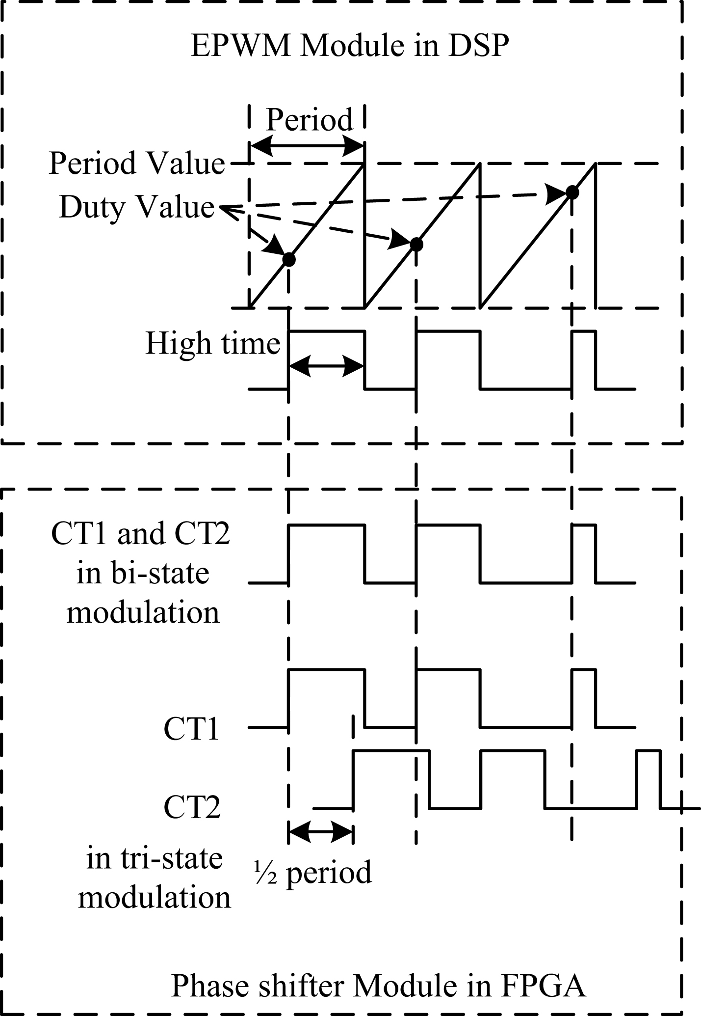
As discussed in Section 2.2, in bi-state modulation, CT1 and CT2 can be same with the original PWM signal, the duty radio in every PWM cycle is decided by period and duty value in every control cycle. While in tri-state modulation, CT2 is the signal with 180 degrees’ phase shift of CT1, as in Fig. 5, which is very easy to be realized in FPGA through shifting register. By adopting synchronous system clock, every shifting register work in the same time domain, and has a fixed delay, corresponding to a fixed phase in fixed modulation frequency, as in Fig. 6. Therefore, we can calculate the number of shifting register to finish the 180 degrees’ phase delay. Although we can design the phase shifter by logic gates. However, the phase shifter in FPGA can be configured by setting the registers in DSP without changing the hardware design, to be more suitable for a unified architecture.
Block diagram of phase shifter.
Current ripple under bi-state modulation
Essentially, the current ripple is the fluctuation in the PWM cycle, and we investigate the ripple characteristic when setting the value of output current as constant. As in Fig. 7,
Coil voltage and current under bi-state modulation.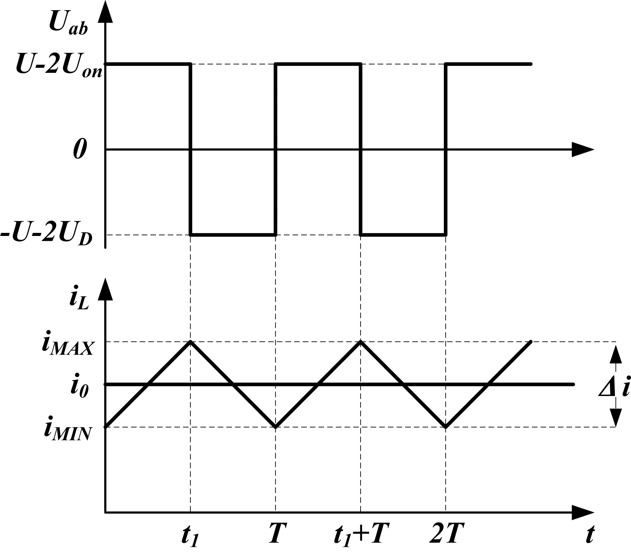
We can get,
Ignore the
Since the time constant of the electromagnetic coil is usually much larger than
Therefore,
Taking the duty radio of 50%,
Then,
From the Eq. (6), it is known that the magnitude of the ripple current is proportional to the power supply voltage of the bus, and is inversely proportional to the switching frequency and the inductance of the electromagnetic coil. In order to reduce the ripple current, it is effective to reduce the bus voltage, but will decrease the dynamic response bandwidth of the DSPA at same time. We must understand how to find the reasonable bus voltage in actual application by effective simulation.
Compared with under bi-state modulation, there is another current remaining process exists under tri-state modulation when
Coil voltage and current under tri-state modulation.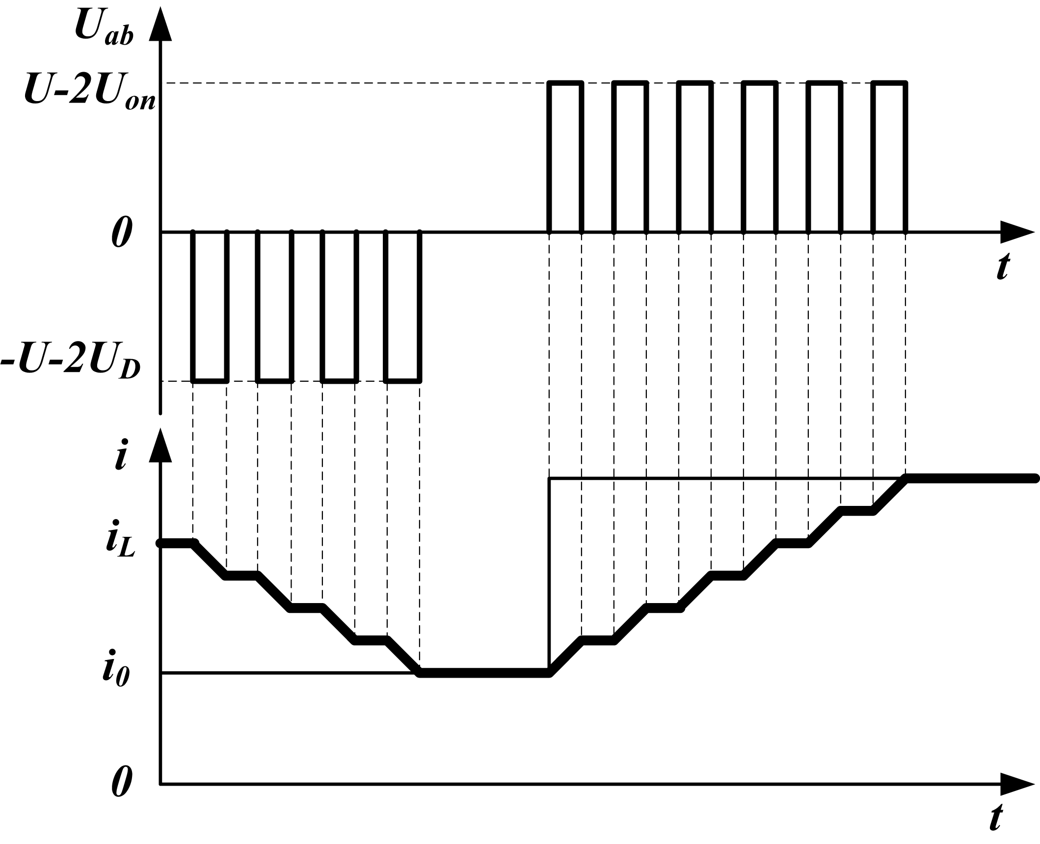
In order to analyze the current ripple, by setting the value of output current as constant, the coil voltage and current are shown in Fig. 9.
Current ripple under tri-state modulation.
The voltage equation of the circuit can be obtained according to the electrical characteristics of the coil, as shown in the Eq. (7).
Where,
We can get:
Then,
According to the Eq. (12), compared with the bi-state modulation, the magnitude of the ripple current of the three state modulation is not affected by the bus voltage of the power supply, but is inversely proportional to the inductance of the coil and the modulation frequency.
But this style of analysis is the ideal condition when constant current outputs, it is only an approximated model, and can only express the ideal condition but not the current ripple performance during dynamic output current in actual application. We developed the simulation approach to describe the current ripple performance during dynamic output current.
From Fig. 7 and Eq. (2), the load voltage is
Where,
Where,
Simulation under bi-state modulation.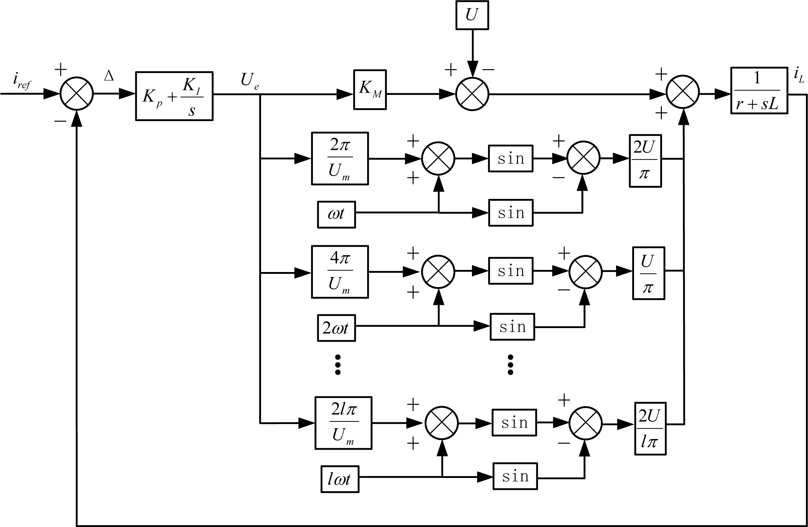
Then,
Simulation under tri-state modulation.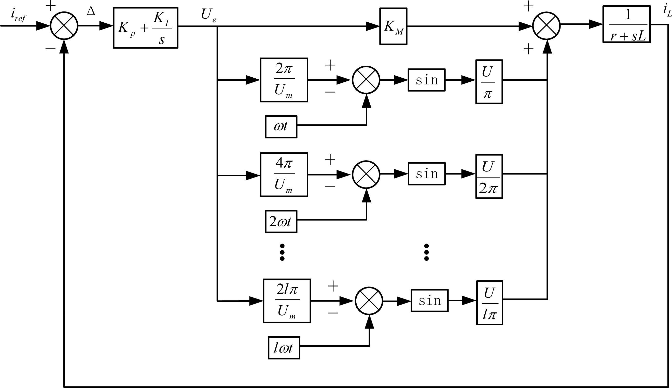
Simulation of load current, (a) desired current commands, (b) load current under bi-state modulation, (c) load current under tri-state modulation.
The relationship between the load voltage and current is
Where,
Parameters in the simulation
Simulation of load current, (a) desired current commands, (b) load current in bi-state modulation, (c) load current in tri-state modulation.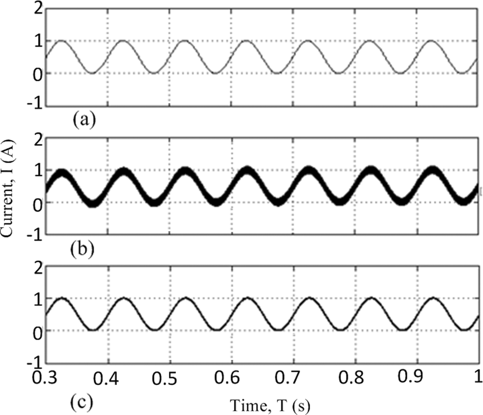
It is very similar to deduce the load voltage expression, from Eq. (7) and Fig. 9,
By Fourier series expansion in Eq. (15),
From Eqs (15), (23) to (25), can get
According to the Eq. (26), the simulation model of DSPA under tri-state modulation was established, as shown in Fig. 11.
Experimental platform.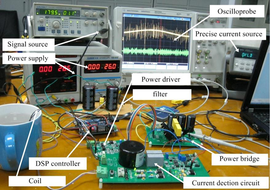
Measured current ripple of 72 mA under desired pulse command, when bus voltage was 20 V, load coil was 6.5 mH, 2.1 ohm, and PWM frequency was 20 kHz, under bi-state modulation.
Current ripple under bi-state modulation with different load coils, modulation frequency and bus voltage: (a) 4.5 mH, 1.6 ohm, 20 kHz modulation frequency, (b) 6.5 mH, 2.1 ohm, 20 kHz modulation frequency, (c) 4.5 mH, 1.6 ohm, 50 V bus voltage, (d) 6.5 mH, 2.1 ohm, 50 V bus voltage.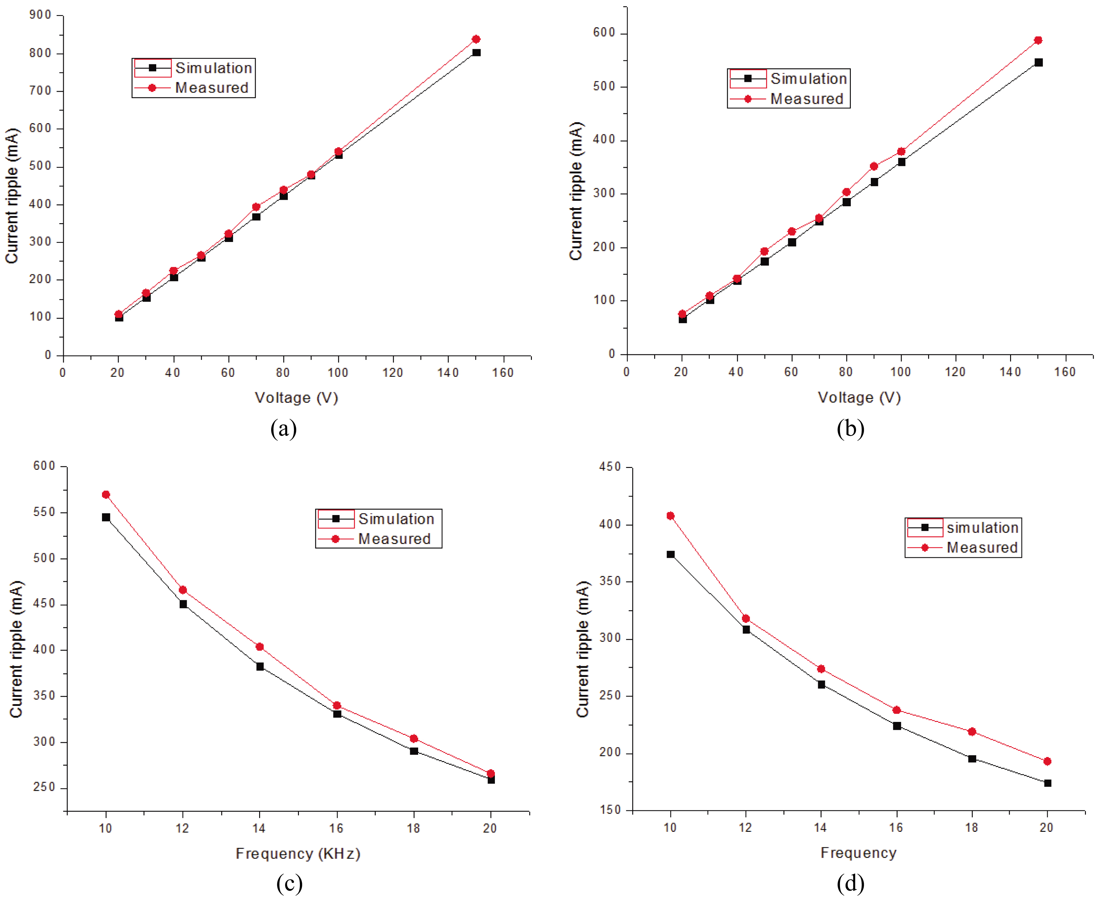
The parameters in simulation are in Table 1. By using step signal and sine signal with peak value of 1 A as the desired current commands, it is easy to verify the outputs following the commands respectively in Figs 12 and 13. Furthermore, it can be seen that DSPA under tri-state modulation has smaller current ripple compared with under bi-state modulation.
To verify the actual ripple performance of DSPA, experimental platform was established to measure the actual ripple value. The experimental platform is shown in Fig. 14, where power supply adopted programmable power, and a power filter was designed to maintain the bus voltage stable and prevent switching noise transmitting into the power supply. Current controller was designed based on TI TMS320F28335 and Altera EP3C25Q240. The whole DSPA structure was based on the unified design in Section 2.
Simulation in Figs 12 and 13 can illustate the current waveform under different condition, and we have measured the actual current ripple, compared with the simulation to verify the effectivity of simulation model, as shown in Fig. 15.
According the relationship in Eqs (6) and (12), Figs 16 and 17describe the compare between measured value and simulation under different bus voltage, modulation frequency and load coils under bi-state and tri-state modulation respectively.
Current ripple under tri-state modulation with different load coils, modulation frequency and bus voltage: (a) 4.5 mH, 1.6 ohm, 18 kHz fixed modulation frequency, (b) 6.5 mH, 2.1 ohm, 20 kHz fixed modulation frequency, (c) 4.5 mH, 1.6 ohm, 50 V fixed bus voltage, (d) 6.5 mH, 2.1 ohm, 50 V fixed bus voltage.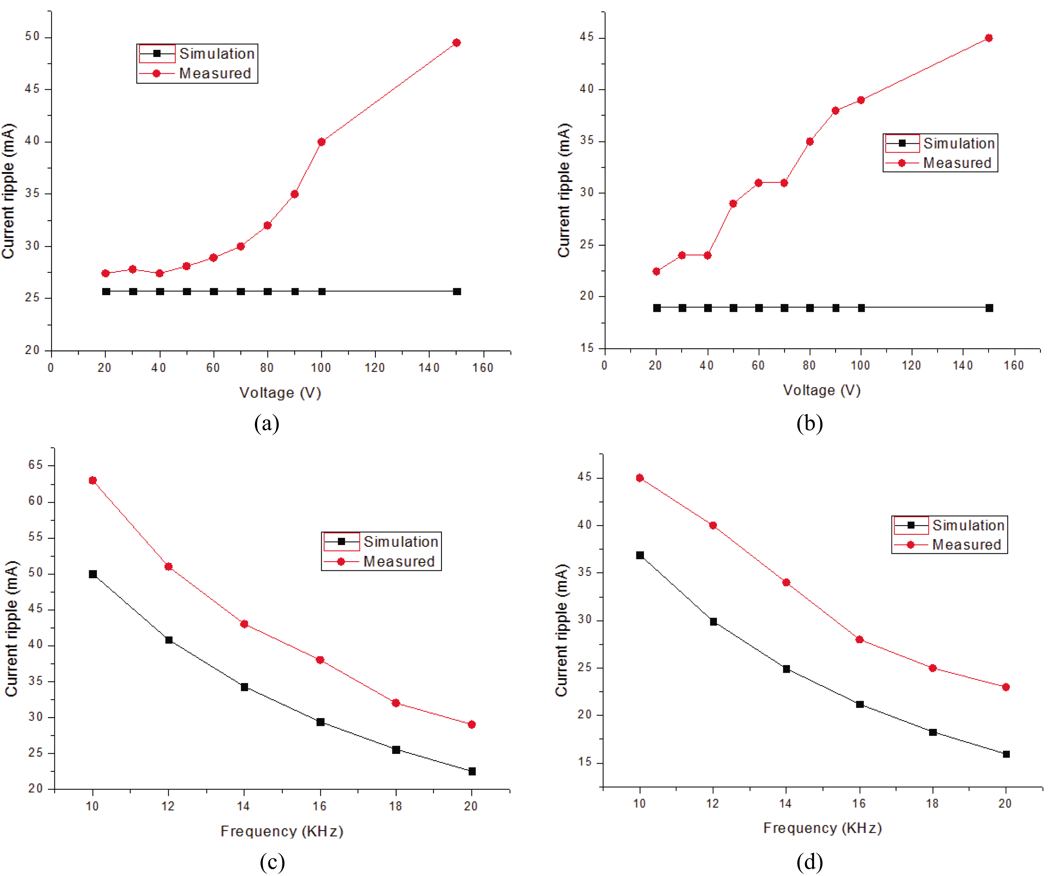
From Figs 16 and 17, simulation can reflect the change trend of the output current ripple, although an error between simulation and measured value is nearly 10 mA magnitude, as in Fig. 17c and d, we believe that the error was caused by the measurement error of actual current measurement process in Fig. 15, for the switching noise will influence the measurement accuracy more with the bus voltage increases. And furthermore, a nearly 10 mA magnitude is relative low and acceptable compared with the requirements in actual application. In general, the simulation and ripple analysis approach is effective in guiding the DSPA parameter design.
In this paper, we proposed a unified design of DSPA in active magnetic bearings, in which the DSPA system can be described as the combinations of the controller, power stage, and the current sensor. By designing a configurable PWM generator, DSPA under bi-state and tri-state modulation can have a unified hardware frame.
A current ripple analysis approach has been proposed. We derive the approximated mathematic express of current ripple characteristic of DSPA under bi-state and tri-state modulation, and design the simulation and experiment. Although a nearly 10 mA magnitude error exists, the general accuracy level is acceptable. The results show approach discussed can effective describe the current ripple characteristic under different bus voltage, modulation frequency and load coils, which can guide the parameter design of DSPA.
Footnotes
Acknowledgments
This work was supported National Natural Science Funds of China (No. 51575411) and the Fundamental Research Funds for the Central Universities (WUT: 2017III046). The authors also thank Zeng Hongyong for his help with theoretical analysis and experimental platform.