
Abstract
At present, the sampling rate in a wireless sensor network is generally low, which does not meet the requirements for high-speed sensor signal acquisition and detection. To address the shortcomings of wireless sensor networks in terms of the design methods and effects assessment, a high-speed wireless sensor network node was designed based on structural health monitoring. Based on the general framework of a wireless sensor node, combined with the requirement of active health monitoring, a test of screws loosening in a reinforced aluminum plate were conducted. The theory of compressed sensing was used to test the effects of compressed sampling for the high-speed acquisition nodes. The results demonstrated that high-speed wireless sensor nodes could complete active excitation, sampling, and processing of the response signal for the application of active structure monitoring with integrated software and hardware and that the system could distinguish the looseness of the screws in the aviation specimens accurately. The nodes also met the requirements of small size, low cost, and low power consumption. The results of the experiment verified that the hardware and software modules for the high-speed wireless sensor nodes functioned and monitored the structural damage effectively. The system solves many key problems of node design in wireless sensor networks in the industrial field.
Introduction
Structural health monitoring (SHM) and wireless sensor networks (WSN) are both hot-spot research topics in the current industrial technology. In recent years, wireless sensor networks have been widely researched in connection with structural health monitoring. To be applied in an active health monitoring system, the features of the wireless sensor node have to include small size, low power consumption, high sampling rate, and active excitation. However, the traditional signal conditioning unit of the piezoelectric sensing element is bulky and inconvenient for the integration of the wireless sensor network into the application system. At the same time, there are also some issues with regard to the physical size and energy consumption of the nodes, which do not meet the requirements of small size and low power consumption. Although some research has been conducted in this area in other countries, the resulting nodes are too large and too expensive, rendering the nodes unsuitable for the requirements of structural health monitoring.
The existing wireless sensor network technology is not suitable for structural health monitoring due to the piezoelectric element. Moreover, the existing methods are not always suitable for many working and experimental environments. In order to explore the application of wireless sensor network technology for structural health monitoring based on the piezoelectric elements, in this study, a high-speed wireless sensor network node was designed and implemented and the function for monitoring the failure of fastening for a reinforced aluminum plate structure was tested. Hence, the design of a special high-speed wireless sensor node was required.
State of the art
Wireless sensor networks have been used to perceive internal structural defects and estimate the damage using structural health monitoring in many fields such as aerospace, shipbuilding, bridge construction, and other fields, and numerous researchers have conducted studies on this topic.
Yuan et al. [1] presented a multiple-channel and multiple-station architecture for continuous real-time data acquisition in wireless sensor networks. Hackmann et al. [2] proposed the MAC Layer Architecture (MLA), a component-based architecture for a power-efficient MAC protocol development in wireless sensor networks and employed a wireless sensor network experiment for a physical beam and in simulations of a truss structure. However, these studies were based on low-speed sampling and high-speed sampling was not considered.
Zhao et al. [3] developed a multi-channel high-speed data acquisition process for a wireless sensor node to monitor actively the responses of a wing structure. Musiani et al. [4] developed high-speed wireless sensor nodes with a sampling rate of up to 10 MPS and demonstrated that the piezoelectric sensor array was effective in their experiment. A design for the multi-channel high-speed sampling for wireless sensor nodes has been developed by the Institute of Computing at the Chinese Academy of Sciences [5]. However, the node power consumption was still high and did not meet the required characteristics of small size and low power consumption.
Furthermore, Musiani [6] originally proposed a high computing power platform. The life cycle of the node was significantly extended by using super capacitors instead of batteries for energy storage. The experiments showed that a 32-bit computational core could run at 100 MIPS for 15 minutes daily. The Chinese Academy of Sciences [7,8] has developed a large volume of nodes. However, these nodes are not suitable for wireless sensors for structural health monitoring applications, and the design of these nodes is relatively unrefined.
The purpose of this study is to solve the shortcomings reported in previous studies. In this paper, specialized high-speed wireless sensor nodes for structural health monitoring, signal testing, and processing were designed and implemented. The theory of compressed sensing was used to test the effects of compressed sampling on the performance of the high-speed acquisition nodes. The test results show that the nodes can be used for active structural monitoring and high-speed signal acquisition, processing, and communication; in addition, the nodes are of small size and have low power consumption.
The remainder of this paper is organized as follows. Section 3 introduces the designs and methods used in this work, Section 4 discusses the tests and results of the paper, and the conclusions are summarized in Section 5.
Methodology
Design of the high-speed wireless piezoelectric sensor nodes
According to the current research status and the demand for structural monitoring, a modular design method was adopted in the design of the high-speed wireless sensor nodes.The modular design was divided into a power module, a stimulating module consist of 555 excitation circuit and DAC circuit, a signal processing circuit, a data acquisition module consist of AD sampling and FIR filtering and processor module consist of external memory and DSP processor, and a wireless communication module [9]. Speak of the excitation module, 555 excitation circuit or DAC circuit is used to generate enough excitation signals for active structure health monitoring. Data acquisition and processing module are intended to monitor the acquisition and processing of response signal actively. The function of the wireless communication module is to send the results of the data acquisition and processing module to the monitoring terminal in the form of wireless network communication [10]. The overall design for the high-speed wireless piezoelectric sensor node is shown as a block diagram in Fig. 1.

Block diagram of the overall design of the high-speed node.
Considering the requirement of active structural health monitoring, the wireless sensor node must have the function of active stimulation [11]. When the customized excitation signal waveform for the structural monitoring application is needed, the incentive method of a DAC (Digital to analog converter) circuit can be used [12,13]. If a higher excitation frequency sine excitation waveform for the structural monitoring applications is required, the 555 incentive method can be considered.
(1) The incentive method of 555 miniaturization
A 555 timer is a device that combines medium-scale integrated analog and digital functions [14]. Figure 2 shows the circuit schematic diagram of a 555 miniaturized excitation circuit. The frequency of the output signal is determined by R
1, R
2, R
A
, R
B
, and C
2 in the circuit, and thefrequency calculation formula is:
The circuit has the advantages of a simple structure, easy implementation, low cost, and low power consumption (about 0.13 W) [15]. It is suitable for the application of wireless sensor nodes and for the research requirements of active monitoring.

Diagram of a miniaturized driving circuit.
The excitation load of the 555 miniaturized driver circuit is a piezoelectric ceramic element with a value of 1.7 nF, which belongs to the capacitive load [16,17]. The circuit can become unstable easily and even generates the phenomenon of self-excited oscillation under the action of a capacitive load. Therefore, in terms of the factors that may lead to circuit instability, two methods were considered to modify and improve to ensure the stability of the drive signal.

Sinusoidal waveform of the output of a miniaturized driving circuit.
a. Buffer the output stage with series resistors
The phase margin of the amplifier is reduced directly by the driving capacitive loads and the phase lag caused by the capacitive loads; the amplifier output impedance will lead to an under-damped impulse response or oscillation. In order to drive the capacitive load directly, the method of cascading resistance at the amplifier output stage to the buffer output level can be used [18]. In this study, we chose to use the operational amplifier CA3140 and the output was buffered through a series resistor. As shown in Fig. 4 and Fig. 5, the burr at the wave crest was smoothed when using the non-buffered waveform.

The non-buffered waveform.

The buffered waveform.
b. Using the AOL curve correction method
In general, the operational amplifier has an internal output resistance of R
0. When it is connected to the capacitive load, an additional pole will be generated in the transfer function of the operational amplifier, which influences the stability of the system. In this study, the internal output resistance (R
0) in the operational amplifier CA3140 is 60 Ω for the capacitance load value of the piezoelectric chip with 1.7 nF. According to Eq. (2), the frequency of the additional pole is 1.56 MHz.
The additional pole, which is generated by the capacitive load has to be a minimum of 10 times higher than the value of the closed-loop bandwidth, otherwise, the system can become unstable [19]. We paralleled a resistor (R L ) between the output and the load to improve the frequency of the additional pole. With this method, the closed-loop bandwidth is 10 times higher. Since the gain-bandwidth of the CA3140 is 4.5 MHz, the frequency of the additional pole must be at least greater than 45 MHz.
Based on Eq. (2) back-stepping, the parallel resistance at the output is 2.2 Ω. Figure 6 shows the schematic diagram of the AOL curve correction method. The following is the formula for the method:
In addition, we joined the level 1:1 isolation circuit between the output stage of the 555 miniaturized driving circuit and the load [20,21], which can also improve the signal. Figure 7(a) and (b) show the output signals of the incentive module with and without the isolation circuit. The output signal stability is improved significantly after adding the isolation circuit.

The AOL curve correction method.

The output signal of excitation module before and after isolation.
(2) The DAC excitation method
The frequency of the waveform for the 555 miniaturized driver circuit has a large range, which can reach 100 kHz. However, only a single sinusoidal waveform can be output, which limits its application for structural health monitoring. In this study, using a DAC circuit resulted in the generation of arbitrary waveforms for the wireless sensor nodes, which greatly expanded the application range of the nodes. Considering the requirement of structural health monitoring and the need for small size and low power consumption for the wireless sensor nodes, the serial DAC chip TLV5618A was chosen in this design.
The TLV5618A is a low-power digital-to-analog converter from Texas Instruments, can operate from a single +2.7 V to +5 V supply, and has a wide dynamic output range. The output voltage of the TLV5618A is obtained by Eq. (4):
The piezoelectric signal conditioning circuit is used for amplifying the sensing signal of the piezoelectric ceramic element and subsequently, the sensor signal is processed by the data acquisition and processing module. The initial piezoelectric sensing signal is small (the positive and negative of only tens of millivolts), while the sampling range of the data acquisition and processing module in AD is 0 V–3 V. Therefore, the piezoelectric sensor signal should be converted into a positive signal first to be amplified with the signal conditioning circuit and the magnification is 50–100 times. The circuit was designed to deal with high-speed signals; therefore, the conversion rate of the op amp should be high enough and the bandwidth should be large enough, but a general-purpose op amp is not suitable for high-speed applications.
In this study, the high impedance operational amplifier CA3140 was selected. The signal conditioning circuit was divided into two stages. The input signal was converted into a positive signal, which was greater than 0 by using an additional circuit.
The circuit is composed of two-stage amplification in order to amplify the weak signal of piezoelectric elements and each stage is based on CA3140 operational amplifier. Firstly, the weak signal is converted into a positive signal in the first stage amplifier; secondly, the converted positive weak signal is respectively amplified g 1 times (g 1 = 10) and g 2 = 1 + R 9∕R 6 times by the first and second CA3140 amplifier; finally, the weak signal is amplified g =10 × (1 + R 9∕R 6) times. The multiplication of g 1 and g 2 is the gain of the two-stage amplifier circuit [22]. The circuit is shown in Fig. 8.

Diagram of the signal processing circuit.

Wiring diagram of the high-speed wireless piezoelectric node.
The data acquisition and processing module is the core of the high-speed node and is responsible for the high-speed sensor signal acquisition, data processing, integration, and communication with the wireless module [23]. Since a large number of high-speed signals were collected and processed through the high-speed node in this application, a DSP (Digital Signal Processing) was chosen as the core component of the data acquisition and processing module because of the superior performance of the DSP in digital signal processing. Table 1 lists some of the parameters of the DSP chips that are commonly used. The TMS320F2812 chip was chosen for the module circuit in the high-speed data acquisition and processing in this study.
TMS320F2812 is a 32-bit fixed-point DSP chip officially launched by TI Company in 2003. It is one of the top-grade DSP in the fields of industrial control and robot control. Compared with the TMS320LF2407A, the performance of the chip has been significantly improved. The chip has not only rich resources, but also a great function to simplify peripheral circuit design.
Its main resources and performance indicators are as follows:
It is the highest performance chip which processing speed is 150 MIPS and has powerful real-time processing ability in C2000 series. It can be applied in many complex control algorithms and its code is compatible with previous DSP models. Therefore, TMS320F2812 DSP has a wide application space. High performance and low power consumption, using 1.8 V internal nuclear power voltage and 3.3 V peripheral interface voltage. The chip which can expand 1M unified address memory and reach 4M addressing space has a 128 K internal FLASH and a 18 K internal SARAM in it. There are three 32-bit timers in the chip. The chip has double event manager EVA and EVB. The chip has two SCI ports and one SPI port, which adds the function of data caching, and the transmission frequency can reach MHz. In addition, the serial communication module also includes enhanced eCAN line and new McBSP, which can meet the demand of a variety of communications. 16 channels of 12-bit A/D. The sampling mode can be set up flexibly. There are 56 programmable and reusable I/O ports can be used.
Comparison of the parameters of commonly used DSP chips
Comparison of the parameters of commonly used DSP chips
The hardware of the data acquisition and processing module mainly includes the DSP and peripheral circuit, the RS232 communication interface circuit, the power circuit and other components [24]. Due to the large amount of data acquired, the high-speed Lamb wave signal, and the inability of the DSP’s built-in memory space to meet the requirements, a static memory IS61LV51216 by ISSI was selected to expand the external memory.
The wireless communication module transmits the data processed by the DSP to the node, which is connected wirelessly to the host computer; the upper computer analyzes the received response signals and monitors the state of the structure [25,26]. In addition, each module of the design of the high-speed wireless piezoelectric node contains three kinds of power supplies (5 V, 3.3 V, 1.8 V). Therefore, a 5-V power supply was used in the node voltage module and the operating voltage of each module was provided by the power conversion chip. Figure 9 shows a high-speed wireless node piezoelectric wiring diagram and Fig. 10 shows a high-speed wireless piezoelectric node object graph.

Physical map of the high-speed wireless piezoelectric node.

Layout of high-speed piezoelectric signal acquisition test.
Test of high-speed piezoelectric signal excitation and acquisition function
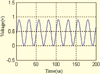
Through the upper section of the design, high-speed wireless sensor nodes can be achieved through the on-chip 12-bit high-speed AD converter to sample and process the high-speed piezoelectric signal. In order to test the high-speed function of the node’s piezoelectric signal acquisition and processing module, a typical aerospace aluminum plate specimen was selected (Fig. 11). The specimen was a 24 mm × 6 mm × 1.5 mm aluminum plate with two piezoelectric plates arranged on the aluminum plate; one was used as the driving element, and one was used as the sensing element. The high-speed node was used to excite the piezoelectric actuator. The piezoelectric sensor received the sensing signal. After the voltage amplification, the piezoelectric sensor was connected to the oscilloscope, and the high-speed wireless sensor node was connected to observe and contrast the results. The high-speed node output (TLV5618A output) excitation signal was 35 kHz and the peak value of the Lamb wave signal was 3.6 V, as shown in Fig. 12 and Fig. 13 for the piezoelectric sensor display of the sensor signals in the oscilloscope.

Output of TLV5618A excitation signal graph.

Piezoelectric sensor signal.
In Fig. 14, the dotted line depicts the acquisition of the high-speed piezoelectric signal in the oscilloscope and the solid line shows the signal collected by the wireless node. The oscilloscope signal and the host computer signal are consistent and the consistency is good in the time domain and the frequency domain.
As shown in Fig. 15 and Fig. 16, the data originating from the SCI serial port was generated to waveform through the upper computer. The upper computer can fully accept the data sent by the SCI serial port, and the serial SCI interface of the node can connect the data collection module and the wireless communication module.

Comparison of piezoelectric acquisition signals in the oscilloscope and the wireless node.
The incentive for the sensor signal for the 40 kHz sinusoidal signals.

The incentive for the sensor signal for the 35 kHz Lamb wave signals.
Wireless sensor network nodes used in structural health monitoring are limited by energy, communication ability, and computing power. In order to reduce the power consumption in the process of high-speed sampling, the theory of compressed sensing was used to test the effects of compressed sampling of the high-speed acquisition nodes [27].
The test signal sequence with a length of 512 was compressed and sampled. Eighty random observations were obtained, and the reconstruction of the signal sequence was realized by using the CosaMP reconstruction algorithm. The process of compressed sampling is shown in Fig. 17.

Compression sampling and reconstruction of signals.
The Test results are shown in Fig. 18 and Fig. 19.

Oscilloscope acquisition based on compressive sensing.

Sine signal acquisition based on compressive sensing.
Based on the results shown in Fig. 18 and Fig. 19, for the 512-point sequence, only 80 points were required to reconstruct the original signal accurately using the method of compression sampling. Therefore, the average sampling rate for the compressed sampling is only 1/6.4 compared to the traditional sampling method [28,29]. In the design of the node, the AD sampling clock is obtained by using the system clock, and the power consumption of the system is shown in Fig. 20.
The power consumption can be reduced by 50% using the method of compression sampling. The purpose of low power consumption is therefore reached, as shown in Table 2.

The relationship between system power consumption and system clock.
Power comparison for traditional sampling and compression sampling
The test results show that the method can be used to reconstruct the signal accurately to reduce the energy requirements of the high-speed acquisition nodes and to improve the reliability of battery life and communication.
In order to test the active structure monitoring ability of high-speed wireless piezoelectric nodes, a typical aviation aluminum plate specimen was selected to monitor the situation under simulated damage. The test specimen was a 24 mm × 6 mm × 1.5 mm aluminum plate, as shown in Fig. 21. Two piezoelectric plates were arranged on the aluminum plate; one was used as the driving element and the other as the sensing element. The miniature excitation circuit was used to generate a standard sine signal with a peak value of 3.6 V and a frequency of 40 kHz to stimulate the driving component and send the signal of the sensing component to the amplifying circuit. The signal was amplified and input into the AD converter and the sampling rate was set to 6 Msps. A digital low-pass filter was used to filter the signal acquisition through the DSP software configuration and the data were transmitted to the wireless module [30,31].

Test aluminum plate specimen.
In the experiment, an absorbing material (sealant) was added between the piezoelectric plate as the driving element and the sensing piezoelectric plate, and the simulated damage of the aluminum plate structure is shown in Fig. 22. Previous experimental experience has shown that the sensing signal amplitude prior to simulation of the damage should be slightly higher than a plus simulation amplitude after injury. The aluminum plate underwent the simulated damage test using the 555 small excitation circuit and the DAC circuit. Figure 23 and Fig. 24 show the results with and without the simulation damage for the 555 circuit excitation sensing signal of the aluminum plate. Figure 25 and Fig. 26 show the respective results for the DAC circuit excited sensor. A comparison of the sensor signals of the two circuits before and after the simulated damage indicates that the peak value of the sensor signal is reduced after the simulating damage, which is consistent with previous experimental results.

Simulated damage of aluminum specimen.

Sensing signal without simulation damage.

Sensor with simulated damage.

Lamb sensing signal without simulation damage.

Lamb sensing signal with simulated damage.
According to the characteristics and demands of active structural health monitoring and the combination with the characteristics of the wireless sensor network, an active structural health monitoring verification experiment was set up based on high-speed wireless piezoelectric sensor nodes. This experiment was composed of a front-end sensor network subsystem and the PC monitoring subsystem. The monitoring structure was a reinforced aviation aluminum plate using piezoelectric ceramic sensors as structure incentives and sensing elements [32,33]. The loosening of the fastening screws on the aluminum plate was monitored. Using high-speed wireless piezoelectric sensor nodes, the data processed by the nodes was transmitted to a computer, facilitating the remote monitoring of the objects by the nodes [34,35]. The software and hardware design of the experimental system are described below.
(1) Arrangement of the testing system
The monitoring object of the front end sensor network system was a reinforced aluminum plate structure (28 mm × 38 mm × 2.0 mm) with screws connecting the reinforcing rib and the aluminum plate [36,37]. On both sides of the aluminum plate reinforcing rib, four pieces of piezoelectric patches (1,2,3,4) were arranged and used for monitoring the identification (1,2,3,4) screws. The experimental setup is shown in Fig. 27.
Based on the amplitude of the sensing signal as the characteristic parameter, a pattern recognition method based on the Euclidean distance was used to monitor the possible non-health factors in the aerial aluminum structure in real time [38,39]. The Euclidean distance calculation formula is:
S ij is the j-th characteristic of the i-th sample in the training sample, S j is the j-th characteristic in the test sample, and D i represents the Euclidean distance between the test sample (S) and the first i-th sample in the training sample.

Experimental monitoring of aviation aluminum plate.

Block diagram of the monitoring system for aluminum plate fasteners.
The system block diagram of the experiment for monitoring the aluminum plate fasteners is shown in Fig. 28. First, the signal generated by the excitation module of the high-speed node in a certain range of frequencies stimulates the piezoelectric sensor arranged on the surface of the aviation aluminum structure, which is actively monitored [40,41]. The response signal of the piezoelectric sensor is received by the node’s piezoelectric signal conditioning module, and the signal acquisition and processing are carried out by the signal conditioning module which is fed into the high-speed DSP module after being adjusted. Next, the processed data is output to the wireless transmission module through a serial port. Finally, the data is transferred to the host computer monitoring the system wirelessly.
The data acquisition and processing module of the high-speed wireless piezoelectric node was polled in turn by the sensor signal of each piezoelectric sensor element, and the data was processed by the wireless communication module for data transmission [42]. The scan module is based on the design of a CD4066 and the chip contains four groups of analog switches. The analog switch is a component that can determine whether an input terminal analog signal can reach the output terminal using the digital signal of the control terminal. The signal at both ends of the switch of the CD4066 analog switch can be used as the input or the output, and this signal has a small conductive resistance, a wide operating voltage range, and small fluctuations in the entire input voltage range. It also has a good frequency response, which can reach more than 1 MHZ. These features of the CD4066 are very suitable for the high-speed sensor signal switching and transmission. Therefore, a CD4066 was used to measure the analog signal of each piezoelectric chip in this experiment.
The scan software program was written in the TinyOS operating system to generate a pulse signal with a pulse width of 50 ms and an amplitude of 3.3 V; the pulse signal was triggered by the analog switch CD4066 [43]. Finally, data acquisition and processing were carried out by controlling the switching-on and switching-off of the CD4066.
The program logic flow of the scan module is:
(1) Initialize Leds, SensorControl, CommControl Interface
(2) Set the generation time of the clock timer
(3) Wait for the timer to generate, if generate interrupts, change the Leds display
(4) Send data, yellow light is triggered, start the counter
(5) PW[0..7] is triggered in turn
(6) Repeat (4), (5)
The logical relationships between the components in the scan module are shown in Fig. 29:

The logic program of the scanning module.

Interface of upper computer monitoring software.
(2) The upper computer monitoring system
The data of the base station node are fused and analyzed by the host computer monitoring system, and the diagnosis of the structure state is obtained [44,45]. Figure 30 shows the interface of the upper computer monitoring software for the port design, Fig. 31 shows the sensing waveform of the high-speed signal, and Fig. 32 shows the flow chart for data processing at the high-speed piezoelectric node.

Sensor signal collected by the host computer.

Flow chart of node work.

The excitation signal of nodes (A) (B) (C) (D) and the sensor signals of the piezoelectric sensors (2), (3), (4).
(3) Experimental steps and results
The specific experimental procedure is as follows:
a. The sine wave (the value of peak-to-peak is 4 V, the frequency is 40 kHZ) was chosen as the active signal to drive the piezoelectric plate when no screws were loosening, and the sensing signal of the piezoelectric patch (2), (3), and (4) were collected and sent to the host computer by using a polling scan.
b. The loosened screws No. 1 to No. 4 gathered the sensor signals of the piezoelectric patches (2), (3), and (4) and sent it to the upper computer; Fig. 33 shows the excitation signal of the node and the sensor signal of the piezoelectric patches (2), (3), and (4). The upper computer took the signal amplitudes as characteristic parameters and the samples were obtained as shown in Table 3.
c. The loosened screws No. 3 and No. 4 (after all the loosened screws were screwed down in step(b)) gathered the sensor signals of the piezoelectric patches (2), (3), and (4) and sent it to the upper computer through the serial port; the computer took the signal amplitudes as characteristic parameters and the training samples were obtained as shown in Table 4.
d. The upper computer calculated the results of the Euclidean distance between the characteristics of the test samples and the training samples using the Euclidean distance method. As shown in Table 4, test samples 1 and 2 respectively represent the loose conditions of the screws No. 3 and No. 4.
The characteristic parameters of the training samples
The characteristic parameters of the test sample
Results of Euclidean distance calculation
In Table 5, test sample No. 1 and test sample No. 2 represent the loose conditions of screw No. 3 and screw No. 4 respectively. The Euclidean distances of the corresponding loose screw No. 3 and loose screw No. 4 are the smallest, which is consistent with the actual situation. The experimental results show that the software and hardware modules of the high-speed wireless sensor nodes are complete and can monitor the damage of the structure effectively.
In order to improve the physical size, the energy consumption, and the low sampling rate of traditional wireless sensor networks, specialized high-speed wireless sensor nodes were designed and implemented for structural health monitoring and for signal testing and processing. The theory of compressed sensing was used to test the effects of compressed sampling of the high-speed acquisition nodes. The conclusions drawn from this study are summarized as follows.
The test results show that the nodes can be used to monitor the active structure, and the described method is convenient for later debugging and maintenance. By using the method of compressed sensing, the signal can be reconstructed accurately, which can reduce the energy requirements of the high-speed acquisition nodes and improve the battery life and the reliability of the communication. When used for active structural monitoring and high-speed signal acquisition, processing, and communication, the system has the characteristics of high sensitivity and good dynamic performance. It can also meet the requirements of small size, low cost, and low power consumption.
The system solves some key problems of traditional wireless sensor networks, such as physical size, energy consumption, and performance, which are significant in the study of wireless sensor networks. However, there are still some aspects that require improvement. A 555 miniaturized driving circuit was used in the design of the stimulating module circuit, which led to the output of a single waveform. In addition, the energy consumption and size can be reduced further. These topics are the focus of future research.
Footnotes
Acknowledgements
This research was financially supported by National Natural Science Foundation of China (Grant No. 51105209, 61401211, 51175267, 61672290), Key University Science Research Project of Jiangsu Province, China (Grant No. 15KJA460004), China Postdoctoral Science Foundation (Grant No. 2012M511760 and 2013T60540), Fundamental Research Funds for the Central Universities (Grant No. 30915118804), National Key Research and Development Plan(Grant No.2017YFF0207200).