
Abstract
We investigated the effects of DC bias current applied directly to the elements on the inclined easy axis thin-film magnetoimpedance element indicating a discontinuous impedance jump. We clarified that the DC bias current contributes to changes in the configuration of domain structure, which induces modification of impedance profiles on the 20 μm-wide element. On the other hand, 40 and 80 μm-wide elements did not show the apparent changes on the magnetoimpedance profiles. The influence of DC bias current on jumping point is not so much, which is attributed to the small bias magnetic field generated by the current; the limited bias level is not high due to Joules heating by the current.
Introduction
Typical magnetoimpedance (MI) sensor is commercially applied as compasses in mobile phones [1], and a number of researches enhance its sensitivity still continue [2–5], to apply it for biomedical applications. In many cases, an easy axis of ferromagnetic material are aligned perpendicular to a high frequency current applied directly to the element, i.e. magnetizing easy axis of the element with small AC field generated by high frequency current, and an external field for detection is applied parallel to the longitudinal direction, the hard axis of the element [7]. On the other hand, discontinuous impedance jumps are obtained when an MI element of thin-film with a uniaxial anisotropy has an inclined easy axis relative to the width of the element, especially when the easy axis angle from the width direction becomes over 50° [8,9], the discontinuous jump becomes significant. This phenomenon is well explained by the simplified domain structure model [10] and discontinuous jump occurs due to magnetization reversal in one domain [9]. This element is expected to be applied for a novel magnetic field sensor like switching elements for detection of a threshold field and the sensor with memory functions [11,12]. For such applications, it is preferable to control a jumping field of impedance. Since a jumping field depends on an easy axis angle and a dimension of an element, it is difficult to control its property after fabrication of the element. A DC bias current applied directly to the element may be a possible way to control a MI profile. The effects of DC bias current on MI profiles with a spiral anisotropy on amorphous wires have been reported [13–15], however, we adopted thin-film elements for compatibility with integrated electronic devices here, and the effects of DC current on thin-film MI elements have less reported [16]. Therefore, we investigated the effects of DC bias current on the discontinuous MI profile of thin-film elements with inclined easy axis and also discussed a potential for controlling jumping point with related to the domain configuration.
Experimental procedure
The rectangular thin-film element using an amorphous Co85Nb12Zr3 film was micromachined by photolithography techniques and sputtering processes. The dimension of sensing parts were 20, 40 and 80-μm wide, 2-μm thick and 3-mm long. The elements were annealed at 400 °C in vacuum with 3 kOe of magnetic field to control their easy axis directions. The sensor element shows a discontinuous impedance jump when the easy axis are oriented from 50°–70° or 75° relative to the width direction. Since our previous studies on the elements showing discontinuous impedance jump was mainly done on 60°-axis element, the easy axis direction was also oriented from 60° relative to the width axis in this study. After annealing for controlling the easy axis of the elements, a Cu/Ti electrode, 2-μm thick, was formed by almost the same way as the fabrication of sensing part, and then the impedance of the elements was measured using a network analyzer (HP8752A) and a wafer probe (Picoprobe 40A-GSG-150-LP) with a 100-MHz AC current and DC bias current applied through a bias tee. Figure 1 shows the dimensions and structure of the fabricated element and the measurement circuit. The centre section of 1 mm was used for the impedance measurement to avoid the effects of demagnetizing effect [17]. The incident AC power was −10 dBm. During impedance measurements, a DC external magnetic field was applied to the element along the longitudinal direction by a Helmholtz coil. The applied DC bias current was altered from −2 to 2 mA for 20-μm wide element and −4 to 4, −8 to 8 mA for 40 and 80-μm wide element, respectively.
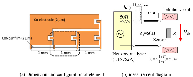
Configuration of fabricated element (a) and measurement diagram for impedance (b).
Figures 2 and 3 show the impedance and inductance profile against an external field when the bias DC current I b applied directly to the element with 20-μm wide. When I b = 0 and the magnetic field changes from −2 Oe to 2 Oe, the impedance is Z = 40 Ω at −2 Oe, and increases gradually with increasing field then drop at around 0.4 Oe. After that, it jumps up at 0.7 Oe, and then decreases gradually with increasing field and becomes 40 Ω at 2 Oe. When the field changes from 2 Oe to −2 Oe, its profile shows a symmetric property with the result when the field changes from −2 to 2 Oe with respect to the axis of impedance Z (Z-axis) on the graph. On the other hand, when I b = 0.5 mA, the symmetric property disappears; for example, at the negative field region, the impedance is almost constant, 38.5 Ω, against the applied field, though the impedance shows higher values in the positive field region. If we apply I b = −0. 5 mA to the element, its profile is symmetric with the results of I b = 0.5 mA with respect to the Z-axis. Inductance also shows similar behaviour; the inductance is L =15 nH at −2 Oe, and increase gradually and then have a broad peak at around −0.2 Oe, then drop at 0.4 Oe. After that it jumps up as same as the impedance jump at 0.7 Oe. When the magnetic field changes in the opposite direction, the profile is a symmetric property with the result when the field changes positive direction.

Applied field dependence of impedance with dc bias current for 20-μm wide element.
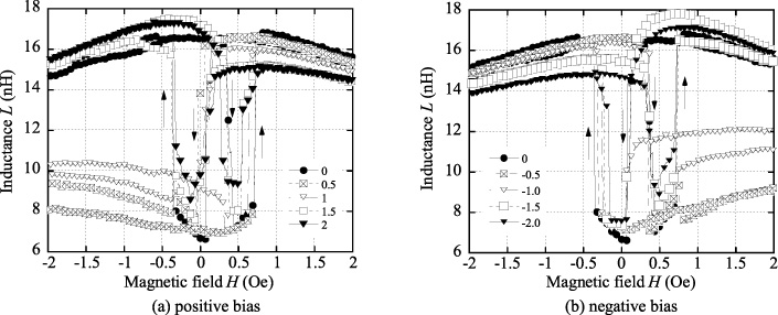
Applied field dependence of inductance with dc bias current for 20-μm wide element.
Figure 4 shows the impedance profile against an external field when the bias DC current I b applied directly to the elements with 40 and 80-μm wide. Compared to the case in 20-μm wide element, the impedance profiles on the 40 and 80-μm wide elements do not change apparently with DC bias current; the profiles do not show asymmetric properties due to DC bias current same as the profiles observed in the 20-μm wide element. (Therefore, the only profiles for negative bias DC current were shown here.)
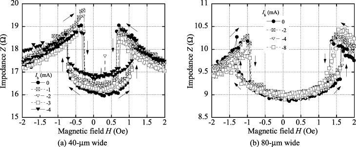
Applied field dependence of impedance with dc bias current.
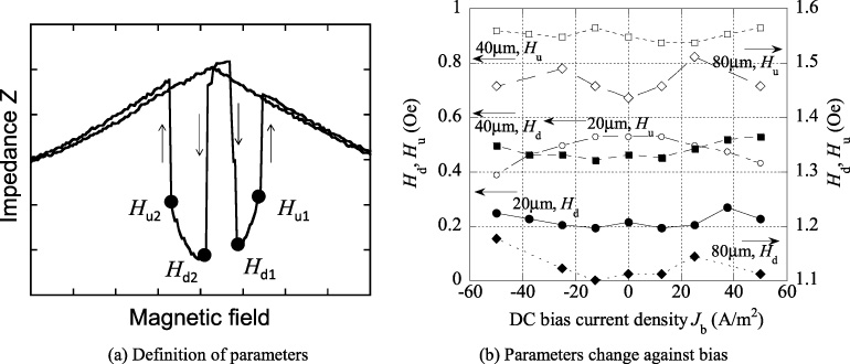
Definition of parameters for jumping field and parameters dependence on dc bias current.
As we are interested in the jumping point in the MI profile of the elements, here, the parameter is defined as shown in Fig. 5(a), and the evaluating parameter is defined as follows:

Domain structures change for 20-μm wide element with and without dc bias current. Applied field alters from −2 to 2 Oe.
In the results of 20-μm wide, the interesting properties were obtained. Therefore, to investigate the relation between domain configuration and impedance changes, the domain changes with applied field and DC bias current were observed with a Kerr-effect microscope. Figure 6 shows the results of domain observations for 20-μm wide element under various applied fields and without bias and with DC bias of 0.5 mA. For the results without bias current, when the magnetization almost saturated and the impedance value is high, the domain shows single domain structure (See (1), (3), (1) ′ and (3) ′ in Fig. 6(a)). We confirmed that the domains become multi domain when the impedance relatively low values (See (2) and (2) ′ in Fig. 6(a)). For the results with 0.5 mA bias current, when the magnetic field is −2 Oe, the impedance is relatively low and domain shows the multi domain, which is completely different from the case without DC bias current. Then, as the applied field increases, the impedance maintains low values, though it shows a small jump around 0.3 Oe, and domain configuration keeps multi domain until the large impedance jump occurs. After the large impedance jump occurs, the impedance becomes high values and the domain shows single domain, which means magnetization almost saturates. The impedance behaviour shows quite different properties between with and without DC bias current, and the discontinuous property strongly depends on the domain configuration. Additionally, further interesting matter is if there is no DC bias, the multi domain parallel to easy axis, i.e., tilted from the width axis, however, multi domain becomes parallel to the width direction around −0.5 to −2 Oe with DC bias of 0.5 mA. We also confirmed that the multi domain appears at lower impedance region and the single domain appears at higher impedance regions in the case of applied DC current of 1 and 2 mA. Although the phenomenon is a bit complicated, further investigation is required for better understanding of this kind of MI phenomenon. As to the jumping point, it slightly deviates due to the DC bias current; this is because several mA of DC current generates very small bias field, which does not contribute to accelerate switching of the magnetization within the domains. On the other hand, the possible current level is limited due to the Joule heating.
The effects of DC bias current on the impedance profile of the thin-film MI element having inclined easy axis were investigated experimentally. The DC bias current modifies the behaviours of impedance changes against the applied field, which is attributed to the alternation of domains configuration. Contrarily, the jumping point shows slight changes; this is because the field level by the current is very small. The acceptable level of DC current is not high due to the heating by the current.