



Abstract
A double differential D-dot overvoltage sensor is proposed based on the D-dot principle for the purpose of faster and more accurate measurement of overvoltage signals. The proposed sensor is a new D-dot sensor structure consisting of four electrodes. It is applied together with the double differential input structure. This structure allows the sensor to operate in self-integration mode and achieve a wide frequency response characteristic while has a stronger anti-interference capability. The simulation demonstration and parameter design are carried out by using the Ansoft Maxwell. A test platform is constructed and used in the steady-state performance and lightning impulse transient-state test of the sensor. Test results demonstrate that the double differential D-dot sensor has satisfying steady-state performances, manifested by small measurement phase and amplitude errors. It can be applied to internal overvoltage measurement of power system. Moreover, the double differential D-dot sensor is equipped with good transient characteristics. The relative error of the lightning wave rise time which is measured by the double differential D-dot sensor is controlled in the range of ±1.7% and the relative measurement error of lightning wave peak is smaller than ±2.0%. It can measure external overvoltages effectively.
Keywords
Introduction
Power grid overvoltage is an important factor that influences safety running of the electric system. Many researchers proposed a lot of calculation models and protection methods for this issue [1–4]. These existing theoretical studies on analyzing the overvoltages of power system are comparatively complete, but over-dependence on simulation datas and lack of measured overvoltage waveforms and parameters, leading to the scientificalness and optimality of research work can not meet the current development requirements of smart power grids. Therefore, there is an urgent need for an easy-to-install sensor for obtaining effective measured datas to promote the development of overvoltage protection research.
Currently, the acquisition of the overvoltage signals of power system mainly depends on the traditional electromagnetic and capacitive voltage dividers [5–8]. These measuring devices are vulnerable to complex electromagnetic and cannot guarantee the authenticity of the signal acquisition due to the limitation of measuring frequency range. Moreover, it has to connect with the primary equipment. A new optical voltage sensor is proposed to realize non-contact overvoltage measurement based on signal transformation [9–12]. Although this sensor has high measurement accuracy, free from electromagnetic disturbance, and has fast response, it fails to improve long-term operation stability, reliability and temperature sensitivity comprehensively and has nonlinear problems during photovoltaic conversion. The authors of [13] studied the non-contact overvoltage sensor that acquires voltage signals through coupling capacitance. However, the coupling capacitance is an energy storage element and is apt to cause oscillation at high frequencies and reflects poor transient response. With the acceleration of smart grid construction, traditional contact overvoltage sensors and optical voltage sensors are difficult to ensure the reliability and economy of overvoltage measurement because of performance defects and cost problems.
The D-dot probe is generally used for electric field measurement and can realize non-contact installation [14,15]. The voltage measurement method based on the D-dot principle has been studied in references [16,17], and the D-dot sensor consisting of three electrodes is designed and improved to a coaxial assembly of three identical copper toroids. It can track fast front-edge transient waveforms, but with small measurement bandwidth. In addition, the inner component of the integrator may cause waveform distortion. The D-dot sensor was also used to measure high-voltage nanosecond pulses [18], and transient voltage waveforms of the pulse power accelerator with a voltage level of 3 MV [19], however, particularly for voltage signals at specific high frequencies. In order to expand measurement bandwidth, the authors of [20,21] improved the traditional D-dot sensor by introducing a method for differential input and multiple parallel electrodes. It can transmit the steady-state voltages at lower frequencies precisely, but often can’t capture high-frequency transient signals which occur quickly. It can be known that there are few studies that apply the D-dot principle to overvoltage measurement, and the sensor that has the proper frequency-response characteristic within a wider frequency range is required to realize the effective measurement of various grid overvoltages.
Therefore, this paper proposes a new D-dot sensor based on the principle of D-dot measurement. The designed sensor is composed of four electrodes and cooperates with the principle of the double differential input method. The symmetric assembly of four arc-shaped electrodes not only has a simple structure and a low manufacturing cost, but also can capture overvoltage signals in a larger spatial range and improve measurement sensitivity. The structure of the double differential input can make the sensor be operated in the self-integration mode with the advantage of large measurement bandwidth, and has a strong anti-interference capability. It has the high accuracy and rapidity to measure the steady state signal and the rapid transient signal without making contact This sensor can satisfy the development requirements of digitization, miniaturization and convenience of the measuring device of smart grids which is suitable for practical applications.
Working principle
Measuring principle of D-dot sensor
The D-dot sensor measures voltage signals by measuring change rate of electric displacement vector. Measuring principle of the D-dot sensor is shown in Fig. 1. Part 1 of Fig. 1 is a metal electrode of any shape and its external surface is A, dA shows the closed gauss surface. Part 2 of Fig. 1 is the grounding insulation, in which the metal electrode is installed. The metal electrode is connected with the grounded equivalent measuring resistance R m through coaxial cable.
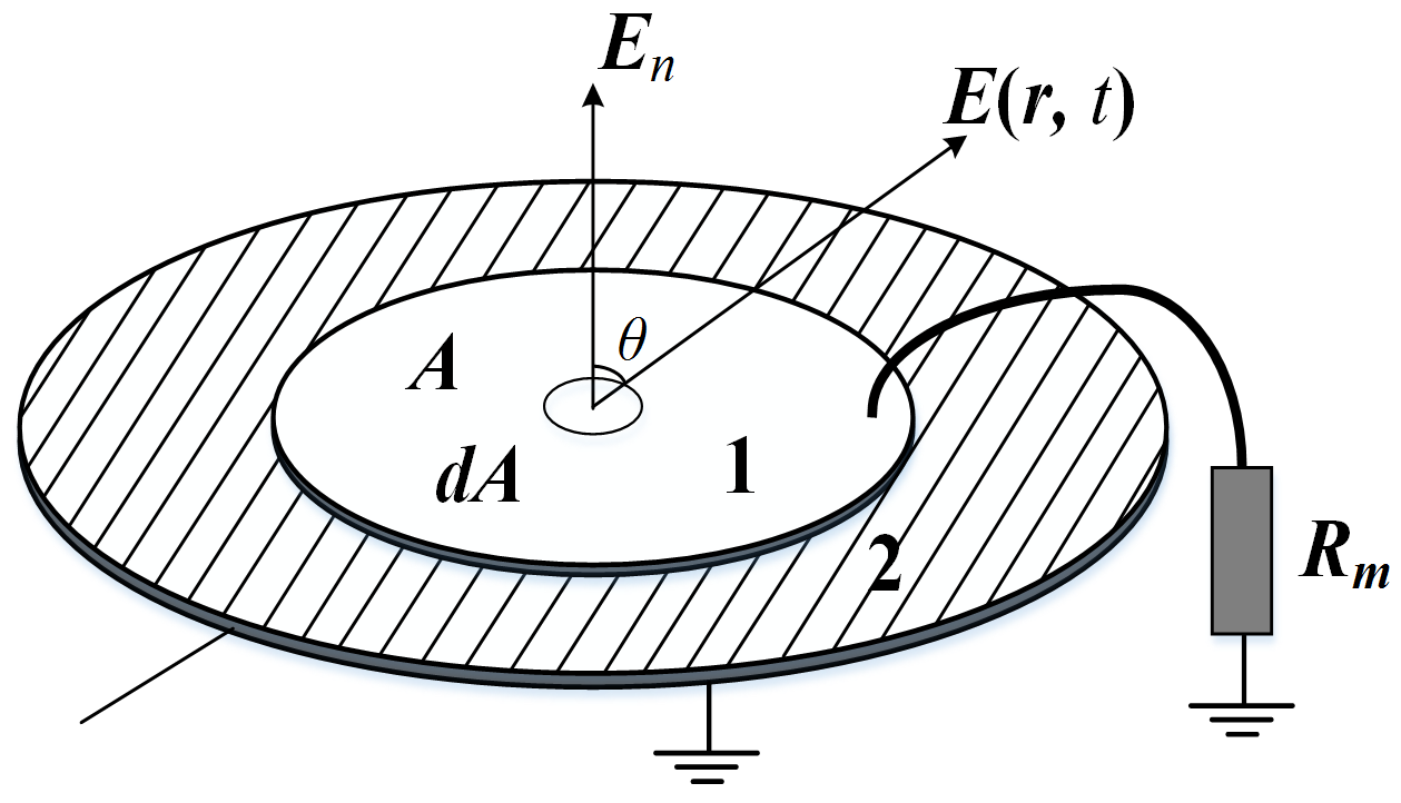
D-dot sensor electric field induction.
In Fig. 1, the sensor is put in a space with the electric field intensity of E(
Most of the voltages of power system are usually in the 50 Hz fundamental frequency range, but the transient voltage frequency may reach the MHz level. To ensure that the sensor can measure the internal and external overvoltages of power system, a broader bandwidth of the sensor is pivotal to reflect the overvoltage signals in a wide range of frequency. Hence, sensors working in self-integration mode present an advantageous performance in measuring overvoltage signals. In this paper, based on the principle of the differential D-dot sensor voltage measurement, the double differential D-dot sensor is designed and investigated for overvoltage measurement Its structure is shown in Fig. 2.
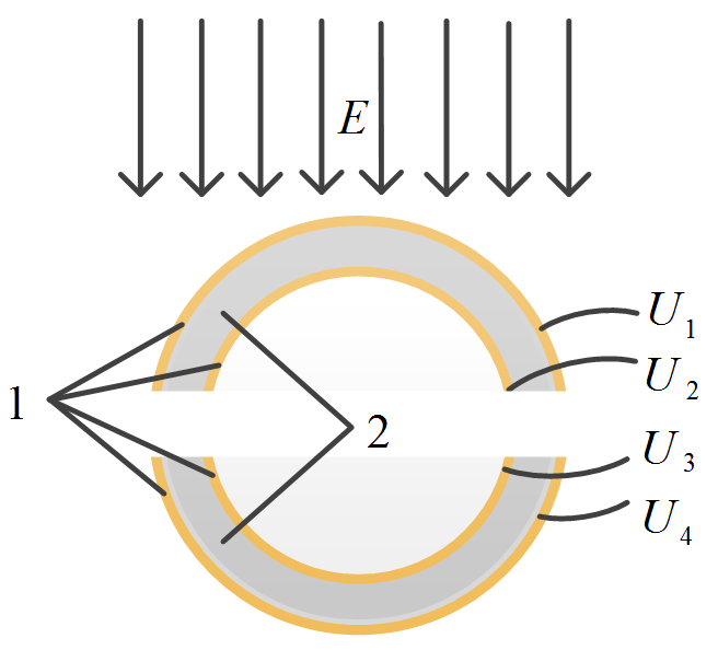
Section view of the D-dot sensor in four electrodes structure.
Part 1 of Fig. 2 shows the section view of the sensor consisting of the four electrodes which are made of copper. The shape of four electrodes are designed as the arc-shaped rectangular sheet. The arc shape is conducive to the Gaussian surface of the outer surface of the electrode being perpendicular to the direction of the conductor surface to be measured, which can increase the equivalent area of the electrodes to improve the measurement sensitivity [24]. In addition, it is similar to the equipotential surface of the electric field around the measured conductor that can make the charge distribution on the electrodes more uniform [25]. The edge effect can be reduced to reduce the electric field distortion caused by the introduction of the electrodes. Part 2 of Fig. 2 shows the insulating material that is filled between the electrodes. Since the sensor is designed to measure the transient signals, in which the lightning overvoltage signal has the characteristics of high frequency, high field strength and high voltage amplitude, the overvoltage measuring device is required to have higher insulation capability. The epoxy resin has a high critical electric field strength, which can make the sensor withstand a higher electric field. On the other hand, it can be used to provide an mechanical support to the whole structure of the sensor owing to its properties, including light weight, wear-resistant and corrosion-resistant [26]. Therefore, the epoxy resin is selected as the insulating medium. To ensure the ease of the sensor fabrication, the inner and exterior electrode sheets are disposed in concentric circles of different radius and fixed on the epoxy resin support. The arrangement of these four electrodes are symmetric around the central cross-section. This also makes it easy to design sensor structure parameters.
The sensor is designed to achieve non-contact measurement by installing under the transmission line, because measuring the voltage of the wire by making the wire go through the center of the sensor will lead to inconvenient installation and bring certain safety risks to operation and maintenance. When the lightning strikes the wire directly or the ground near the wire, each electrode of the sensor can realize overvoltage measurement by measuring the rate of change of the electric displacement vector. In comparision with the differential D-dot sensor, the structure of four electrodes increases capture and reaction capability to overvoltage signals. The output signals of four electrodes are processed by the two-level differential amplifier, as shown in Fig. 3.
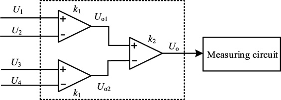
Signal measuring principle of the double differential input.
In Fig. 3, U
o1, U
o2 can be expressed as:
In Eqs (2), (3) and (4), R m1 and R m2 are the input equivalent resistances of two first-level differential amplifiers, respectively; A eq1 to A eq4 are the equivalent area of the four electrodes from the top to the bottom; k 1, k 2, and k 3 are the difference-mode magnification times of three differential amplifiers, respectively.
Equation (4) shows that the difference-mode signal amplifying power is the product of magnification factors of two-level differential circuit. The double differential D-dot sensor can improve the common-mode rejection ratio and signal-to-noise ratio (SNR) significantly, so that the sensor has a greater immunity to interference signals. This makes the sensor more adaptable, which is propitious to the sensor to obtain more effective measured data in the actual installation and operation environment. It also ensures the ability of the sensor to amplify the signal to be measured, which facilitates the monitoring of weak voltage signals and improves the measurement sensitivity of the sensor. Moreover, most of the operational amplifiers can ensure that the input equivalent resistances R m1 and R m2 reach the G𝛺 level or higher, hence, the self-integration condition [20] can be satisfied easily and the introduction of the integrator circuit is avoided. Finally, the signal U o is processed by the measuring circuit. It consists of the data acquisition unit and signal processing unit based on some commonly used technologies.
When the sensor is placed under the wire for measurement, the equivalent circuit parameters of the sensor can be obtained, as shown in Fig. 4.
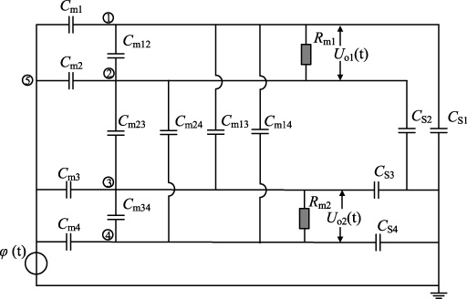
Equivalent circuit of the sensor.
In Fig. 4, nodes ①, ②, ③ and ④ are the four electrodes of the sensor from the top to the bottom in Fig. 2; Node ⑤ is the measured wire potential; C
m1, C
m2, C
m3 and C
m4 are the mutual capacitances between four electrodes and the wire to be measured; C
s1, C
s2, C
s3 and C
s4 are the stray capacitances from four electrodes to the ground; C
m12, C
m34, C
m13, C
m14, C
m23 and C
m24 are the mutual capacitances between the electrodes. R
m1 and R
m2 are the input equivalent resistances of the differential amplifier for measurement. Since the output singals of the ① and ② electrodes are processed to get a differential output U
o1(t) and the output singals of the ③ and ④ electrodes are processed to get a differential output U
o2(t), it can be known from the reference [20] that C
m12 and C
m34 introduced by the differential input method have the significant impact on the performance of the sensor. Although there are C
m13, C
m14, C
m23 and C
m24 under the structure of the four electrodes, their influence on the output of the sensor can be almost negligible. In order to simplify the analysis and more effectively research the sensor performance, the effect of C
m13, C
m14, C
m23 and C
m24 on the sensor output will not be considered. Finally, the expression of the transfer function of the sensor is given by:
Where:
The output of the sensor based on the equivalent circuit can be obtained from Eq. (5), and the performance of the sensor are further quantified, which can provide a design basis for determining the structural parameters of the sensor.
Simulation model
In analysis of the optimization of the sensor, as simulation of the sensor is featured by large field domain but small research entity. What’s used in this paper is finite element method with favorable adaptability in irregular region for more accurate calculation results [27–30]. Therefore, the structure of the sensor is optimizied by using the Ansoft Maxwell, an electromagnetic field finite element computation software. Considering actual installation conditions, the epoxy resin support is designed as a hollow cylinder. Four copper sheets are installed inside and outside the hollow cylinder. The simulation model of the sensor is shown in Fig. 5. Meshes under non-uniform distribution are adopted as units to implement finite element method for calculus of variations [31], and its mesh figure of Y–Z and Z–X plane is shown in Fig. 6.
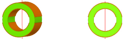
Simulation model of the double differential D-dot sensor.
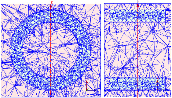
Mesh figures of Y–Z and Z–X plane for sensor model design.
To determine the size of the sensor, the single-phase 3D model is built to research the relationship between the sensor’s capacitance parameters and the structural parameters of the electrodes, as shown in Fig. 7. In Fig. 7, the measured wire is set at the distance of 1.5 m from the ground, and the voltage is set to 10 kV. The measuring points should be in the vicinity of the conductor region due to that the electric field strength decays rapidly along the radial direction of the wire. Therefore, the sensor is placed under the transmission wire at 20 cm from the wire to avert insulation device from being destroyed. The simulation settings are as follows: region size is set 100% of the calculation model, and border region calculation is set zero to simulate the situation wherein the electric field at the infinite point is zero.
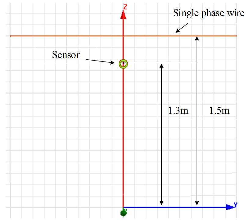
Single-phase 3D model of the double differential D-dot sensor.
To verify whether the structural design and materials of the double differential D-dot overvoltage sensor are satisfying to solve the problems of electric field distortion and insulation, the distribution of the electric field around the sensor at a 10 kV power frequency voltage is simulated, as shown in Fig. 8.
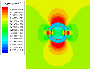
Electric field distribution of the double differential D-dot sensor.
It can be seen from Fig. 8 that the whole model is projected onto the Y–Z plane. The electric flux density between the electrodes of the sensor is about 6907 C/m2. When the sensor isn’t put into the electric field, the electric flux density of the same region is about 7178 C/m2. Then, the electric field distortion rate is 3.78%. Therefore, the placement of the sensor can result in the distortion of electric field under the wire slightly. Moreover, datas in Fig. 8 show that the highest electric field intensity is 10.029 kV/m. The maximum electric field strength that the epoxy resin filled between the electrodes can withstand is about 35 MV/m, which is way bigger than 10.029 kV/m. This finding means that the material and structural design of the sensor will not be broken down by a high electric field.
Based on the simulation model, the specific parameters of the electrodes are analyzed to more effectively design the parameters. Due to the symmetry of the structure, the upper two of the electrodes of the sensor are selected to show the parameters to be designed. Figure 9(a) shows the parameters of the electrode itself. l 1, l 2 are the arc length of the electrodes. d 1 is the thickness of the electrodes. d 2 is the width of the electrodes, which is the main factor influencing the equivalent area of the sensor. The width and thickness of these four electrodes are the same. Figure 9(b) shows the parameters between the electrodes. The inner diameter r 1 of the outer electrode and the outer diameter r 2 of the inner electrode must be determined, which can affect the sensor size and the spacing D between the electrodes. It can be known from reference [20] that the differential input introduces the equivalent mutual capacitance between the electrodes. By freely adjusting the spacing between the electrodes, the phase difference and voltage divide ratio can be adjusted more effectively and conveniently. Therefore, d 2, D are major parameters during the design of the desired sensor.
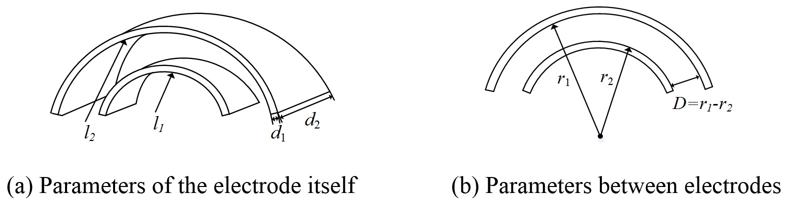
A schematic diagram of the parameters of the sensor.
When a transient voltage of 10 kV is applied to the wire, the peak value of the induced voltage at 20 cm from the wire when the sensor is not placed can be simulated and calculated to be 8.75 kV. The signal processing hardware circuit used in this paper has an input range of ±5 V, so the voltage divide ratio is at least 1750. This can be used as a design basis for the sensor output. The parameters of the sensor are designed by researching the relationship between the capacitance parameters in the equivalent circuit of the sensor and the major parameters d 2, D of the sensor, so as to satisfy the measurement requirements of the overvoltage signals. The mounting position of the sensor is fixed, so that the mutual capacitance between the measured wire and the electrodes is basically unchanged. The variation of the stray capacitance from the electrodes to the ground is almost negligible compared to that of the mutual capacitance between the electrodes. Hence, the mutual capacitance between the electrodes, C m12, is calculated, when the electrodes width d 2 and the spacing D between the electrodes are adjusted respectively. The relationship curves are obtained, as shown in Fig. 10(a,b).
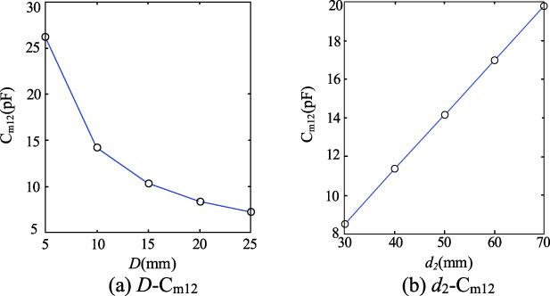
Relationship curve between equivalent capacitance and electrode parameters (a) D-C m12 (b) d 2-C m12.
In Fig. 10(a,b), the trend of the curves illustrate that the smaller spacing and larger width of the electrodes can both increase the mutual capacitance values. The main structural parameters d 2, D of the sensor can be adjusted to change the sensor’s capacitance parameters according to the relationship curves in Fig. 10. Correspondingly, the sensor’s capacitance parameters are calculated through simulation and substituted into Eq. (5) to realize the change of the sensor output. Based on this, the structural parameters are adjusted to make the sensor obtain acceptable partial pressure and good linearity to ensure the output signal of the sensor in the input range of the amplifier for digital measurement. On the other hand, the amplitude-frequency response and the phase-frequency response of the sensor are calculated to ensure that the sensor can work with large measurement bandwidth and high measurement accuracy in a smaller volume. Thus, the structural parameters of the sensor can be determined, as shown in Table 1.
Design parameters for the double differential D-dot sensor (unit: mm)
The datas in Table 2 are substituted into Eq. (5), and the amplitude-frequency response and the phase-frequency response curves of the sensor can be simulated using Matlab software. The results are shown in Fig. 11. As can be seen from Fig. 11, the sensor has a stable gain in the range of 1 Hz to 15 MHz at least and the phase error is close to
Capacitance parameters of the sensor
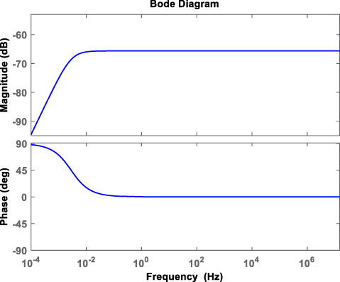
Amplitude-frequency and phase-frequency response of the sensor.
To demonstrate the measurement accuracy of the sensor at the steady state and response characteristics at the transient state, the time domain waveforms of the sensor input and output are simulated at 10 kV, 50 Hz sine wave excitation and 10 kV, 1.2/50 μs standard lightning wave excitation. The results are shown in Figs 12 and 13. In Figs 12 and 13, U i is the measured voltage, whereas U o is the sensor output voltage.

Steady-state simulation waveform of the sensor input and output.
Based on above simulation results:
It can be seen from Fig. 12 that the amplitude error between U
i
and U
o
is smaller than 0.5%, as well as almost no phase delay exists between U
i
and U
o
. In Fig. 13, under the 1.2/50 μs standard lightning wave, the relative error of the lightning wave rise time of U
i
and U
o
is approximately 1.2%, reflecting the response of such sensor to the transient voltage waveform is relatively fast.
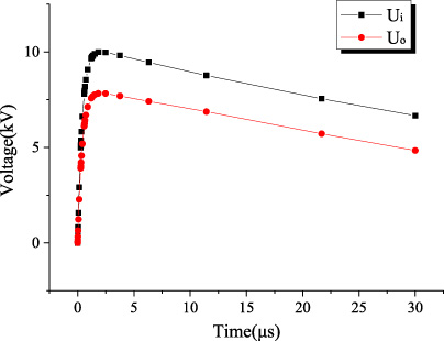
Transient-state simulation waveform of the sensor input and output.
Construction of test platform
After the demonstrations of the design and simulation outcomes, a 10 kV voltage test platform is constructed with the aim of evaluating model performance. The schematic of test platform structure is shown in Fig. 14.

Schematic of test platform structure.
A long straight copper rod with a length of 1.5 m and diameter of 1 cm is taken as the single-phase transmission conductor. According to the position of the sensor and wire in the process of simulation analysis, the copper rod is put at 1.5 m from the ground and the test sensor is installed at 20 cm under the rod. Coaxial cable is used to connect the output terminal of the sensor to the signal processing circuit. The set-up transformer connects to the copper rod. The voltage of the transformer with an output frequency of 50 Hz is adjusted by the regulator to test the steady-state performance of the model. A 10 kV lightning impluse voltage generator is used as a standard lightning overvoltage source for verifying the transient characteristics of the sensor and its type is a SUG255X. This is the impulse voltage test waveform commonly used in the test [34]. The high-voltage probe is applied as a standard device to realize the calibration of the designed sensor and the probe type is a Tektronix P6015A. This probe can measure pulse signals up to 40 kV peak, has a 75 MHz measurement bandwidth and has a rise time of 4 ns, enabling it to capture fast high-voltage signals. Thus, it can be used as standard contrast signal of this experiment. The relative amplitude and phase position of waveforms are compared on a 1 Gs/s, 75 MHz Tektronix oscilloscope (OSC) by measuring the output signals of the high-voltage probe and sensor simultaneously [32].
The test platform scene is shown in Fig. 15. The steady-state test and lightning impulse transient-state test are performed on this platform. The test model of the sensor is manufactured according to the model parameters obtained by the simulation referred before in Part 3. The practical sensor is shown in Fig. 16.
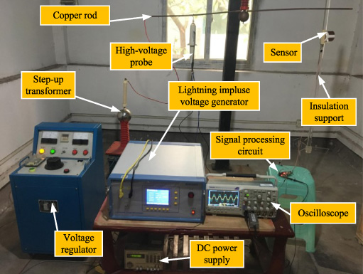
Test platform scene.
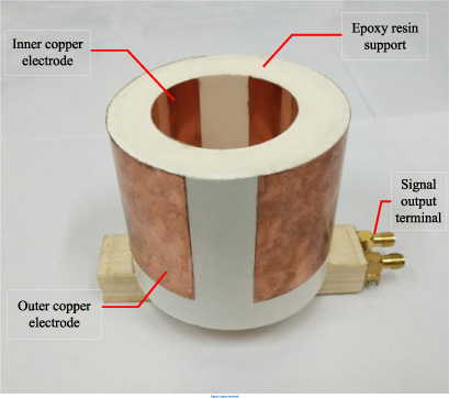
Sensor test physical picture.
On the above test platform, the transformer is regulated by the voltage regulator to raise the wire voltage from 1 kV to 12 kV. The wire voltage is measured directly by the high-voltage probe with the attenuation ratio of 1000:1. The oscilloscope channel 1 shows the output waveform of the designed sensor, whereas channel 2 shows the high-voltage probe. The waveform comparison between the high-voltage probe and sensor when the wire is applied with a phase voltage of 6 kV is shown in Fig. 17.
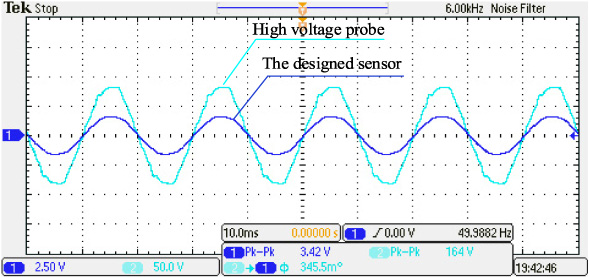
The steady-state measurement waveform when voltage is 6 kV.
It can be seen from Fig. 17 that the error of the waveform phase of the sensor and high-voltage probe is less than
The output voltages of the high-voltage probe and sensor are fitted. The fitting curve is shown in Fig. 18. The U S (CH1) is the effective value of the sensor output and U H (CH2) is the effective output voltage of the high-voltage probe which is converted to the primary side. Figure 18 shows that the output voltage of the sensor has a good linear proportional relationship with external voltage. The linearly dependent coefficient R 2 = 0.9989, indicating the good degree of linearity of the sensor input and output. Based on this result, the sensitivity of the sensor under the steady state operation can be approximated as the slope of the output-input characteristic curve, which is 0.209 V/kV. This sensitivity value can meet the design and use requirements of actual overvoltage measurement [33]. These results demonstrate that the sensor has satisfactory steady-state performance, enabling the detection of internal overvoltage signals.
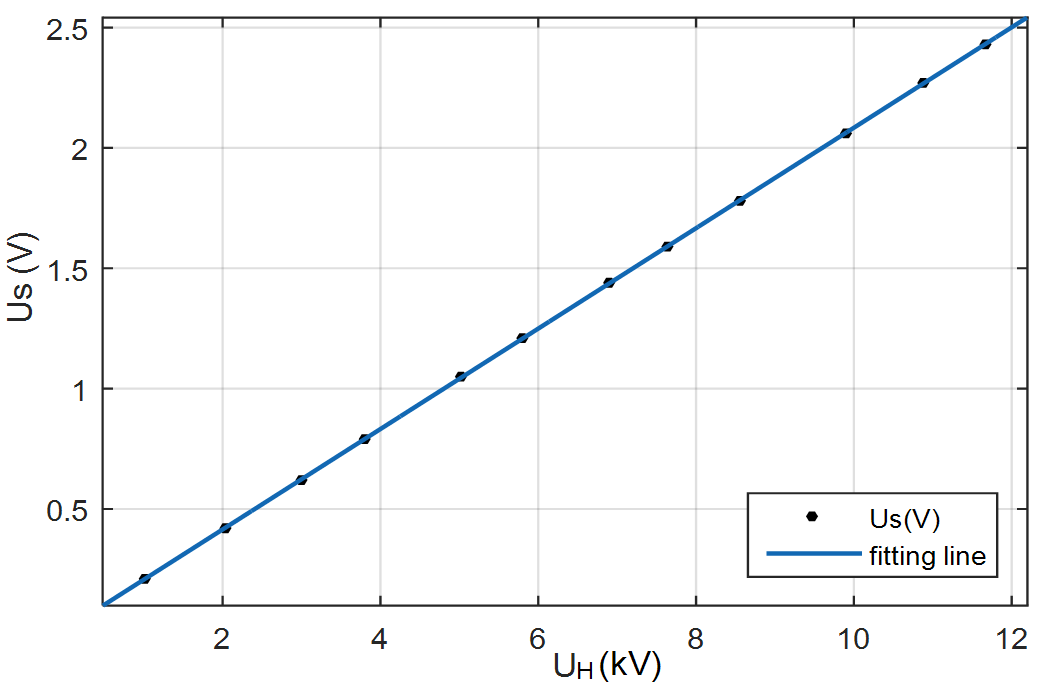
Linear fitting curves between the sensor and high-voltage probe.
A 1.2/50 μs standard lightning wave with a peak voltage of 2 kV–10 kV is generated by 10 kV lightning impulse voltage generator. The lightning waveforms measured by the sensor and high-voltage probe when a peak voltage of lightning wave is 5 kV, 8 kV and 10 kV successively are shown in Fig. 19.
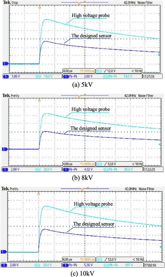
The transient-state measurement waveform of the sensor and high-voltage probe.
The rise time of lightning wave could be observed from the measured waveforms to ascertain transient response speed. The corresponding relative errors can be calculated. The results are shown in Table 3. In Table 3, T S-pk (CH1) and T H-pk (CH2) are the lightning wave rise time measured by the sensor and high-voltage probe.
Test results of rise time of lightning wave measured by the sensor
The peak voltage values are monitored and recorded for analyzing the accuracy of the sensor, as shown in Table 4. The voltage divide ratio of the sensor is approximately 2000:1. It can be obtained according to the ratio of the linear fitting curve of the datas in Table 4. Then, the relative error is calculated. In Table 4, U S-pk (CH1) and U H-pk (CH2) are the lightning wave peak voltage measured by the sensor and high-voltage probe.
\relax\pagebreak Based on above test results:
In Fig. 19, the designed sensor can track the measured waveforms well, and transmits the measured signal without distortion or noise. It can be seen from Table 3 that the relative error of the lightning wave rise time measured by the sensor is controlled within ±1.7%. As stipulated in the IEC61000-4-5 standard [34], the proposed sensor can meet the requirement of rapid response speed to lightning wave. It can be seen from Table 4 that given the standard lightning wave with a peak voltage of 2 kV–10 kV the relative peak error of the output of the sensor and high-voltage probe is smaller than ±2.0%, which reflects the high measurement accuracy of the sensor to the lightning voltage amplitude. The results from the transient-state test show that the measurement bandwidth of the sensor can reach up to MHz, also it can maintain a stable gain in a broad frequency range and avoid the oscillation of high frequencies.
Test results of peak voltages of lightning wave measured by the sensor
A non-contact double differential D-dot overvoltage sensor based on the principle of electric field coupling is designed. A theoretical study and analysis are carried out. Based on that, the sensor structure and relevant circuit are established. The simulation calculation is performed to design the sensor parameters and verify the rationality of the sensor structure. Finally, the experimental platform that is used in the steady-state performance and lightning impulse transient-state test of the sensor is constructed. Results demonstrate that the designed sensor can measure steady-state signals quickly and accurately. Moreover, it owns excellent transient performances, which exhibits rapid response speed to lightning signals and reflects high measurement accuracy. The sensor has a large measurement bandwidth, which can be applied to the measurement of the internal and external overvoltage signals of power system. The proposed sensor achieves miniaturization with a simple structure and a lower cost, as well as non-contact digital measurement that makes the installation of the sensor more convenient. It can satisfy practical engineering demands and the development trends of smart power grids.
In future research, the influence of adjacent electric field will be considered to research decoupling method of achieving three-phase voltage measurement. Futhermore, air temperature, humidity and polluted sensors will be taken into consideration when experiment are carried out to get environmental influencing factors on the voltage divide ratio of the sensor and research the method of compensation.
Footnotes
Acknowledgements
This work was supported by the National Natural Science Foundations of China (Grant No. 51677009) and Chongqing science and technology plan project (Foundation No. cstc2017jcyjAX0181).