



Abstract
Based on the invalidation and damage of the field effect transistors under lightning radiation, we establish the breakdown experiment with open-circuit voltage wave and the protection experiment with TVS as the protection device. The junction field effect transistor and the metal oxide semiconductor field effect transistor are used as material. We draw some conclusions. In the breakdown experiment, the breakdown voltage of the MOSFETs is higher than that of the JFETs as a whole. The MOSFET can be adopted in the amplifier circuit which is expected to get higher input resistance and breakdown voltage. The drain-source resistance can recover to the original resistance value after being placed a period of time, but the gate-source resistance is irreversible. The invalidation of the device under test is due to the breakdown of gate-source. The TVS can protect the FTEs well. The change of pin resistance of the MOSFET is inconspicuous. MOSFETs are more stable for debugging and development of the amplifier circuit. The results provide some significance for the development and improvement of the lightning electric fields change measuring instruments in the future.
Introduction
Lightning is a common phenomenon in nature. The earliest research about lightning can be dated from Benjamin Franklin’s kite experiment in the early 18th century. Over the past 200 years, numerous researchers have been studying the lightning physics. They are trying to make a scientific explanation for the occurrence and development of lightning and making many achievements. However, a mass of phenomena about lightning are not completely understood, which requires great efforts of generations. The spectrum of electromagnetic wave emitted by lightning is very wide; therefore, the detection of electromagnetic wave becomes an important way to study lightning. Using the detection results of the lightning electric fields change measuring instrument, the lightning electric fields waveform can be inverted the characteristics of the lightning electric fields. The lightning detection plays a huge role in the study of lightning. Therefore, the improvement of the lightning electric fields change measuring instrument is significant [1,2].
Field effect transistor (FET) fits in with the requirement of application of electronics for its advantages in noise, thermal stability and radiation. For decades, with the development of new devices and the improvement of the FETs’ technological level, FETs have become one of the most vital semiconductor devices [3,4]. In the article “Optimization of a power mosfet and its monolithically integrated self-powering circuits”, H. Nguyen-Xuan, L. Gerbaud, et al. presented an integrated semiconductor device designed by the power MOSFET, and optimize its physical structure [5]. Robert Coffie introduced the simplified field plate model for field-effect transistors in the article “Slant Field Plate Model for Field-Effect Transistors” and obtained the method of improvement of electric fields management [6]. X. Li et al. expatiated the principle of TVS in the article “Analysis of the Impulse Withstand Performance for Transient Voltage Suppressor”, and analyzed the withstand capability [7]. The above authors made detailed research and optimization on the integrated device and protection device, but did not analyze the damaged reason of the FET itself and the protection measures.
In this paper, we use an open-circuit voltage wave to conduct the breakdown experiment on the junction field-effect transistor (JFET) and the metal oxide semiconductor field effect transistor (MOSFET). Using the TVS protect the field effect transistors. The breakdown voltage of devices and the pin resistance before and after invalidation are processed, and the invalidation reasons of the device are analyzed. It is found that the MOSFET which is more applicable for amplifier circuit. This provides a reference value for the development and improvement of the lightning electric field change measuring instrument in the future.
Theoretical analysis
FET is a kind of semiconductor device which controls the output current by the input voltage. It is the voltage control device which has the high input resistance and almost no current in the input. The insulator layer between the gate electrode and channel of the FET is susceptible to breakdown-voltage. It is easy to cause the breakdown damage between gate and sources due to the external electrostatic voltage, especially the withstand voltage between gate and sources is only dozens of volts. With various testing techniques, analytical instruments and methods, the invalidation process of the FETs can be defined, the invalidation mode or mechanism can be identified, and the final reason of invalidation can be determined, which provides a basis and approach for improving the reliability of devices. There are six invalidation types of FET from mechanism analysis [8,9].
The first type of invalidation is the electrostatic high voltage makes the gate of MOS devices be breakdown which causes the input end failure. Figure 1 is a cross-section diagram of MOS field effect transistor. As seen in Fig. 1, the aluminum gate is insulated by the thin layer of SiO2. Because of the great insulation performance of SiO2, the input impedance of the MOS devices can reach more than 1012 Ω. Such a high input resistance prevents the static charges on the gate from being released via leakage current, but accumulates on the gate. As can be seen from the figure, actually, it constitutes a parallel-plate capacitor between the gate and channel. Since the input capacitance of the MOSFET is small, the accumulative micro charge can make the voltage rise to a high level, which creates a problem whether the SiO2 thin layer can withstand voltage. Exceeding the withstand voltage limit, the SiO2 thin layer will be broken. The result of the breakdown is that pinholes are formed on the oxide layer, which makes the gate and the channel to connect and causes the device to damage.
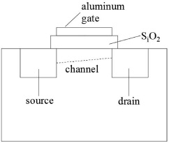
Transverse section of the MOSFET.
The second invalidation is the discharge between adjacent aluminum strips, which causes short-circuiting or open-circuiting between adjacent leads (aluminum strips) of large-scale and very large-scale circuits. The voltage between adjacent aluminum strips may overstep the air breakdown voltage of gap to generate the electric spark in the presence of static electricity. This phenomenon is more likely to occur when the edge of aluminum strips have burrs. The aluminum strips melts which causes short-circuiting or open-circuiting after the discharge occurs. The third condition is that the static high voltage makes the dielectric breakdown between the circuit layers of the multilevel metallization, which causes the lead (aluminum strips) to short-circuiting or open-circuiting and damages the devices.
The fourth condition is that the PN junction melts due to the electrostatic discharge current, which leads the device parameters to degrade or invalidate [10]. The area of the PN junction is shrinking because of the decrease of the integrated circuit component size. The current allowed to flow is correspondingly decreasing, while the current caused by static electricity is sometimes large. The paper carries out quantitative analyses to the emitter junction as an example. When a current pulse flows from the emitter through the emitter junction to the base terminal, the current has power consumption in both the emitter junction and the base region (because the resistance of base region is higher than emitter region, the emitter region resistance is not considered). Since the two regions with power consumption are close together, they have an impact on the temperature rise of nearby silicon. The total power consumption near the PN junction is:
Where, V D is the voltage drop at both ends of the junction, which whether is a reverse breakdown voltage or a forward voltage drop, depends on the direction of the current. R B is the resistance of base region.
If the body is initially charged to some static potential V, which is subsequently discharged through the device, the resulting current flow i will be an exponentially decaying pulse of the following value:
i is the function of time, exponentially decaying with time. Where, I p is the initial (peak) value of current. τ is the circuit time constant in seconds. A sketch of the relationship between the current and time is shown in Fig. 2 [11].
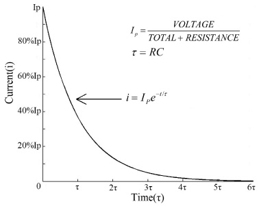
Current and time for a discharge of static electricity.
Substitute the formula (2) into (1).
This is an expression for instantaneous power. Since the power has been consumed approximately 99% during 5τ time, we calculate the average power within 5τ time. To simplify the calculation, we assume that V
D
and R are constants (actually, they are related to temperature).
The average power density is P AV ∕A. Where, A is not the area of emitter junction. Instead of the full emitter junction area carry current, the current essentially flows from the edge of the emitter to the base contact due to the current crowding which takes place during the rapid transient pulse. Therefore, the area to be used for the power density calculation, A should be the cross sectional area of the current path in the base i.e., the emitter length times the base junction depth [11]. A = L E X jB.
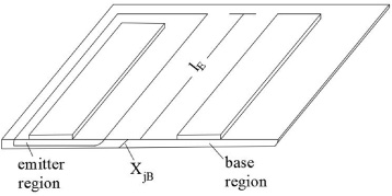
The structural map of emitter junction.
How much power density the PN junction can bear was studied by Winston and Bell. Theoretically, the PN junction damages when the temperature reaches the melting point of silicon. Based on the one-dimensional heat conduction theory, the researchers deduce the following formula:
Where, K is the thermal conduction coefficient, 𝜌 is the density, C P is the specific heat, T m is the actual temperature, T i is the initial temperature, t is the width of time pulse and P/A is the power density of damaged PN junction. We can figure out how much current the device can bear under different pulse widths when the parameters of it can be known.
The fifth condition of invalidation is that the large current fuses the aluminum strips. The electro-static discharge current causes the partial of aluminum strips overheat, which makes the aluminum strips melt and open circuit. The sixth condition is the electro-static discharge current causes the resistance of thin layer fuses or makes the resistance value change and invalidate.
Main parameters of the FETs
According to its structure, the field effect transistors can be divided into the junction field effect transistor (JFET) and the metal oxide semiconductor field effect transistor (MOSFET), among them, MOSFET can be divided into depletion-mode and enhancement-mode. All types of FET are available in N-channel and P-channel [12–14]. The FETs used in our experiment are N-channel depletion-mode JFET 3DJ6F and 3DJ7F, N-channel enhancement-mode IRF620 and P-channel depletion IRF9610 MOSFET. Each device is experimented with 4–8 samples.
The most important parameters of JFET are the pinch-off voltage (V
P
), the drain saturation current (I
DSS
) and the transconductance (g
m
). Refer to the parameter manual to get the parameter indexes of 3DJ6F and 3DJ7F: V
P
< 9 V, I
DSS
= 1∼3.5 mA, 3DJ6F g
m
> 1 mS, 3DJ7F g
m
> 3 mS. The experimental circuit diagram of test parameters is shown in Fig. 4 [15,16]. The test method is to adjust the potentiometer (R
W
) and measure V
G
and V
D
at G and D points with a multimeter. According to the formula
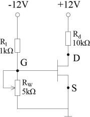
Parameters circuit diagram of JFET under test.
According to the measured JFET parameters, Fig. 5 shows the transfer characteristic curve. From the figure, we can get the parameters of JFET under test. V P ≈ 0.58 V, I DSS ≈ 1.1 mA and the g m is approximately equal to 2.2 mS when the V G is −0.3 V.
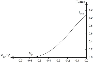
Actual measurements of JFET transfer characteristic curve.
Using the WQ4832 transistor curve tracer, the characteristic curves of MOSFET IRF9610 and IRF620 were measured as shown in Fig. 6. The transistor curve tracer shows that the x axis is 1 V per grid and the y axis is 100 mA per grid.
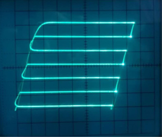
The characteristic curve of MOSFET.
This experiment adopts open-circuit voltage wave to be the voltage source and the GDS 3502 digital stored oscilloscope is used to collect and store the received waveform. The experimental circuit diagram is shown in Fig. 7 [17,18]. Select every kind of model number FET 3∼4, test the quality with WQ4832 transistor curve tracer, and measure the resistance of drain-source and gate-source with the multimeter. Connect the open-circuit voltage wave and the oscilloscope to both ends of the transistor pin. The breakdown experiments of the drain-source and gate-source pins are carried out in two cases. First, the other pair of transistor pin is in open-circuit. The open-circuit voltage is applied from 0.5 kV until the FET is broken down, and the step length is 0.2 kV. When the waveform changes, the voltage value recorded at this moment is the breakdown voltage of pin under test. Second, access 9 V reverse bias voltage to another pair of pins and make it working. Repeat the above experiment and record the voltage value when the pin is broken down. After the breakdown experiment, select 2∼3 transistors of FET again, connect a 9.1 A TVS in parallel at both ends of the pin under test. The other pair of pin is respectively set to open-circuit and applies reverse bias voltage. Connecting circuit, the open-circuit voltage is applied from 1 kV to 5 kV with 0.5 kV step length. After each impact, take off the FET and test to whether it is damaged with the transistor curve tracer. Measure and record the resistance of drain-source and gate-source again. The following figure shows the four measurement conditions with four model number of FET.
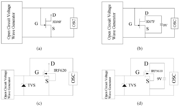
Circuit diagram of experiment. (a) Pin breakdown under open-circuit. (b) Pin breakdown under applied voltage. (c) Under open-circuit, the pin under test in parallel with TVS for breakdown. (d) Under applied voltage, the pin under test in parallel with TVS for breakdown.
The typical waveforms in the experiment are shown in Fig. 8(a), (b) and (c). Where (a) and (b) are the typical waveforms of 1.2/50 μs open circuit voltage when the impact voltage is 0.7 kV and 1.5 kV. And (c) is the waveform when the device is broken down. It can be seen that the waveform is significantly distorted and the FET has been damaged. In the experiment, we use 3∼4 field effect transistors of each model. The breakdown voltages of different pins under different conditions are averaged to process, the results as shown in Table 1. Because the gate of MOSFET is isolated by insulator (such as SiO2), we can be seen from the table, when the same pin is measured under the same condition, the input resistance is higher than that of JFET and can be more than 109 Ω. Therefore, the breakdown voltage of MOSFET is 200∼1000 V higher than JFET. For the same pair of pins, the breakdown voltage under the applied voltage is lower than the breakdown voltage under open-circuit, in which the JFET is little difference. Under the open-circuit condition, the breakdown voltage of JFET is about 50∼100 V higher than that under the applied voltage, and the MOSFET is 200∼600 V higher. According to the operating principle of FET, as the width of depletion layer increases, the conductive channel will be narrowed and the breakdown voltage will decrease. In addition, under the same conditions, the breakdown voltage of the drain-source and gate-source is not much different. It can be concluded from Table 1 that the MOSFET can be adopted in the amplifier circuit when we wish to get higher input resistance and breakdown voltage.
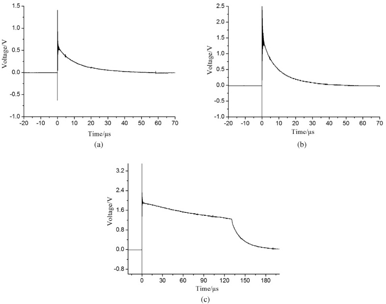
The typical waveforms of FET when impacted and breakdown. (a) Voltage waveform when 0.7 kV. (b) Voltage waveform when 1.5 kV. (c) Voltage waveform when the FET is breakdown.
The breakdown voltage of pin of devices under different conditions
The resistance value of each pin before the test and after the breakdown is measured. Table 2 shows that the resistance value of one of the each transistor before and after the breakdown, where “−” indicates that the resistance value is too large to exceed the range. We deem that the resistance value is infinite.
Resistance values before and after different pins breakdown
In the experiment, we found that the breakdown pin of drain-source recovers to the original resistance value after being placed for a period of time, in which the resistance value of JFET after recovery is slightly lower than that before the experiment, but the resistance value of MOSFET is slightly higher than that before the experiment when the transistor recovers under the applied voltage at both ends of the gate and source. This phenomenon is beyond our expectation. We speculate that the reason might be that the channel layer between gate and drain of the MOSFET is degeneration, which results in the resistance and the breakdown voltage increases. Testing the invalid FETs with the transistor curve tracer, we can found that the drain-source saturation current is significantly smaller than the current of normal device from the I-V curve of the damaged device, as shown in Fig. 9. This also proves from the side that the gate itself is not damaged, but the area between the gate and the drain has a problem.

The characteristic diagram of damaged MOSFET.
It also can be seen from Table 2 that the breakdown between drain and source of the JFETs has little effect on the drain-source resistance, but the gate-source resistance slumps significantly. However, the breakdown between gate and source not only greatly decreases the gate-source resistance, making the region between the gate and drain almost short-circuit, but also considerably reduces the drain-source resistance. The junction field effect transistors of N channel and the metal-oxide semiconductor field effect transistors of IRF620 have the greatest diminution in drain-source resistance. In addition, the breakdown of gate-source is irreversible. Therefore, according to the data in the table, we can deem that the damage of the FETs is due to the gate-source breakdown caused input invalidation.
In order to establish the lightning observation network, we use the FET to amplify circuit, and a new method of lightning electric and magnetic fields change measuring instrument is developed. When the lightning occurs, the vertical electric fields around the metal circular plate change. According to the principle of induction, the induced charge on the metal circular plate will have change accordingly. The variational charge signal obtained by amplifier circuit is transformed into the voltage signal, which can obtain the changes that the vertical electric fields near the ground caused by lightning, thus the lightning in detection range can be located. To prevent the electromagnetic radiation and transient overvoltage from damaging amplifying circuits and FETs, TVS (Transient Voltage Suppressor Diode) can be used as protective devices. Its main parameters are shown in Table 3.
Model number and main parameters of TVS
Model number and main parameters of TVS
The JFET of model number 3DJ7F and MOSFTE of IRF9610 are connected in parallel with the TVS. Figure 10 shows the resistance values of each pin of device under different conditions. The experiment shows that the TVS can provide good protection for FET. We increase the impact voltage to 5 kV, the pins are not broken down basically and the transistors are not invalidation. Figure 10(a) shows respectively the changing curves of resistance value which the pins of drain-source and gate-source after each impact. It can be seen from the figure that the drain-source resistance of JFET is decrease with the increase of impact voltage as a whole. In addition, after applying the voltage at both ends of gate-source, the drain-source resistance tends to a phenomenon that the curve is decrease first and then increase. But the overall trend is decreasing. The reason is that the potential of source side depletion layer increases with the increase of the voltage at both ends of the drain-source, which results in the electric fields of source side enhance. Under the effect of the source side electric fields, the number of current carriers entering the depletion layer rises and the current increases. At this moment, the source side depletion layer extends more towards the source (close to the source side basically), thus the resistance of drain-source decreases. When the gate-sources are applied with the increasing voltage as the measured pin, due to the lower voltage of drain-source, the potential of the source side depletion layer is low. The source side depletion layer is less extended to the source, which causes the resistance of drain-source is large. Because the gate-source resistance of MOSFET exceeds the measurement range of multimeter, we consider the resistance of gate-source to be infinite.

The resistance changing curves of different pins before and after breakdown under different conditions. (a) The resistance changing curves of 3DJ7F pins of drain-source and gate-source after each impact. (b) The resistance changing curves of IRF9610 pins of drain-source after each impact.
Figure 10(b) is the resistance changing curves of the IRF9610 drain-source after each impact. It can be seen that for the MOSFET, the change of resistance value is flat relatively before the pin is breakdown. With the increase of the impact voltage, the increase or decrease in resistance is not significant.
Each model number of FET is tested using multiple transistors. During the protection experiment, minority JFET is damaged, while MOSFET is not. Accompanied by a charred pungent odor, the invalid JFET appears the phenomenon that the pin is melting and the parameters of device are degradation. And both the resistances of drain-source and gate-source are drop to several tens of ohms. Using the temperature gun, we measure the temperature of pin rises to 1450 °C. Considering the edge crowding effect of emitter current, the temperature of the edge part of the source might be higher. This temperature is far more than the melting point of silicon 1413 °C and thus the device is destroyed. This phenomenon of invalidation is the condition that the partial overheating caused by electrostatic discharge current melts the PN junction, which leads the device parameters to degrade or invalidate. Therefore, we deem that the MOSFET is more stable for debugging and development of the amplifier circuit.
In this paper, we use the open-circuit voltage wave to conduct the breakdown experiment on the JFET and the MOSFET. Using the TVS protects the field effect transistors, and the resistance changes of each pin are recorded and analyzed. The following conclusions are obtained through experiments.
(1) Through the breakdown experiment, it is found that the breakdown voltage of the MOSFET is higher than that of the JFET as a whole. In addition, for the same pair of pins, the breakdown voltage under the open-circuit is higher than that of under applied voltage. Therefore, the MOSFET can be adopted in the amplifier circuit when we wish to get higher input resistance and breakdown voltage.
(2) We test the resistance value of the pins of device under test before and after the breakdown, the drain-source resistance can recover to the original value after being placed a period of time. But the gate-source resistance is irreversible. The invalidation of device is due to the breakdown of gate-source input.
(3) The TVS can protect the FTE well. The change of pin resistance of the MOSFET is not significant. MOSFET is more stable for debugging and development of the amplifier circuit.