
Abstract
Flexible cooking surfaces, eg. fully active surfaces, have gained lately an increasing importance in the domestic induction heating. Multi-inverter structures are a cost-efficient solution to develop this technology. However, they add control restrictions that can be solved with a power factor corrector (PFC) stage as proposed in this work.
The proposed converter and modulation strategy work with zero voltage switching (ZVS), decreasing the switching losses, enabling a higher working frequency and, therefore, decreasing the magnetic devices size. The bus voltage is controllable and can be increased, easing the load power control and decreasing current through load and inverter and, so, the power losses. Besides, the switching frequency is constant in the mains cycle and can be modified to synchronize the load inverter and the PFC stage avoiding intermodulation noise. A 3.6 kW prototype has been implemented fulfilling the EMC requirements. The experimental waveforms and efficiency have been measured to prove the feasibility of this proposal.
Keywords
Introduction
In recent years, induction heating (IH) technology has become a reality in our homes [1–5]. This cooking technology has been developed in depth, and it has revolutionized the cooking way. In comparison with typical technologies, such as gas, electric or halogen, IH is more efficient, faster, cleaner and safer [6].
Recently, flexible cooking surfaces have taken importance in the domestic IH technology [7]. There are different types of surfaces with concentric coils or with coils spread along the whole surface, which are denominated fully active surfaces (Fig. 1). These allow heating several pots, no matter the size or shape of these.

Fully active surface [17].
The coils from a typical IH cooktop are supplied by an inverter, usually a half-bridge, which is the most common topology in these applications. However, the development of flexible cooking surfaces has brought an increase of the manufacturing cost due to the increased number of coils and power electronics devices. In order to achieve a cost-effective implementation, some multi-inverter structures have been proposed recently [8–10]. However, these structures add control restrictions and complicate the power control in the induction loads [2].
In order to overcome these restrictions, a power factor corrector (PFC) front-end stage has been proposed. The PFC stage assures a power factor close to the unity, a low harmonic distortion and generates a controllable DC voltage bus. This stage allows separating the mains front the multi-inverter structure, fulfilling EMC requirements [11–16] and making easier the control of the output power in the pot [17–19]. Besides, the bus voltage can be increased, decreasing the current through IH inverter and IH load, and, therefore, decreasing losses in these devices.
Furthermore, having into account that induction heating cooktops with fully active surfaces have usually two isolated electronic board because they are powered from two mains phases, and in order to reduce manufacturing cost implementing multi-inverter structures, it is interesting to join both electronic boards. This idea can be implemented with a front-end PFC to get a common DC bus. In this way, the total board size and several components such as DC-DC, relays, digital electronic components or heatsinks can be reduced.
The paper is structured as follows. The next section presents the topology of the converter and the operation mode, the control strategy section describes how the converter control is performed. After that section, the implementation and the experimental results are shown and, finally, the main conclusions of this work.
Converter topology
The proposed PFC converter is shown in Fig. 2. It is based on the boost converter and it is composed of two half-bridge legs, a and b, which allow short-circuiting the boost inductance, L b , with the mains voltage, v ac , with a period T ac , and/or the bus voltage, v b . Each half-bridge is composed of two switching devices, S h and S l , implemented with IGBTs, T h and T l , and antiparallel diodes, D h and D l . A filter between the mains and the PFC stage is placed, supplying the medium frequency currents and removing the high ripple of the boost coil current, i ac . In the proposed implementation, an inductor, L f , and a capacitor, C f , are used for filtering. Besides, a capacitor, C b , filters the bus voltage, which powers the IH inverter. The set is composed of as many half-bridge branches, Sh, n and Sl, n, as IH loads. Each IH load [20] is composed of the series equivalent resistance, Req, n, and inductance, Leq, n, and the resonant capacitor, Cr, n.
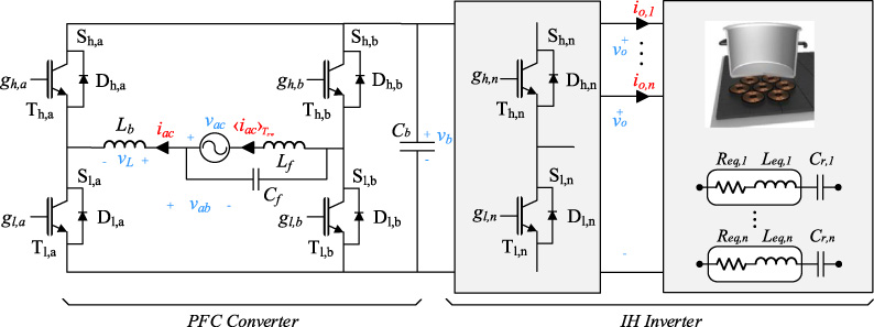
PFC IH topology with n IH-loads [19].
The PFC converter works in full-bridge configuration in order to get Zero Voltage Switching (ZVS) and fixed-frequency Continuous Conduction Mode (CCM) as is shown in Fig. 3. In this way, the Th, a device and the Tl, b device are activated simultaneously, and vice versa. Therefore, the boost voltage, v
l
, according to the activated devices is

ZVS and fixed-frequency CCM modulation strategy [17].
The converter control consists on generating a sinusoidal reference current, if, ref, in phase with the mains voltage and with the desired RMS current value, If, rms. The regulator adjusts the mains current, i f , to follow the reference exactly. The main advantage of using the control of the current managing the duty cycle, D a , is the converter can work at constant frequency avoiding intermodulation noise between IH inverter and PFC stage. This duty cycle must be controlled in order to get a sinusoidal mains current waveform in phase with the mains voltage. In this way, a good power factor and a low total harmonic distortion of the current is achieved.
In order to control the system and to eliminate the stationary error, a proportional, Kp, and integral, K i , regulator is proposed. In typical control schemes, the action calculated by the regulator is directly the duty cycle, D a , applied to the PFC stage. However, this system is difficult to control using this scheme because its non-linearity which depends strongly on the mains voltage, the bus voltage, and the induction load.
To overcome this issue, using the boost coil average voltage, V
L
, as controller output action is proposed, as it is shown in Fig. 4. When the average voltage in an inductance differs from zero, it means a lineal variation of its average current according to the differential equation that models the boost coil behavior. Consequently, the V
L
voltage makes possible to control the boost coil average current, I
b
, linearly and, therefore, the mains current, i
f
, can be properly shaped. Keeping in mind Eq. (2), the duty cycle can be calculated in a second step as

Control scheme where the calculated action is the boost inductance voltage, V L , which is used to calculate later the duty cycle by using the converter parameters [18].
In order to perform this control, the input voltage, v ac , the input current, i f , and the bus voltage, v b , must be measured.
Prototype
In order to prove the feasibility of the proposed topology, a 3.6 kW prototype with one IH load has been designed and implemented. The operating frequency has been set to be higher than 20 kHz to avoid acoustic noise. The final prototype is shown in Fig. 5. It is composed of a three-phase module, FS150R12PT4, with three half-bridges on parallel using 1200-V Infineon IGBTs. A Spartan-6 FPGA from Xilinx is used to implement the control architecture. Besides, the whole system can be managed from the PC through a Wi-Fi module and a PC application has been developed using Visual Basic.
The 150 μH boost inductance, L b , and the 200 μH filter inductance, L f , have been implemented as 10 cm diameter air core toroids with 43 and 50 loops, respectively. The current is measured with the CDS4050 magneto-resistive current sensors from Sensitec and the voltage is measured using resistive dividers. The analog to digital conversion is performed using a 10-bit and 1-MSPS ADCS7477 converter from Texas Instruments.
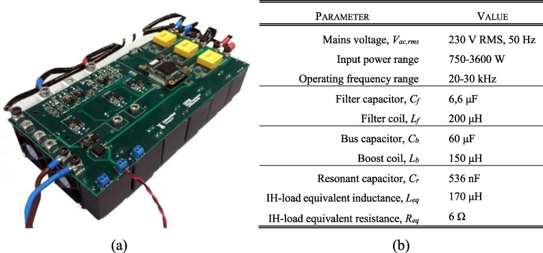
Experimental prototype (a) and converter design parameters (b).
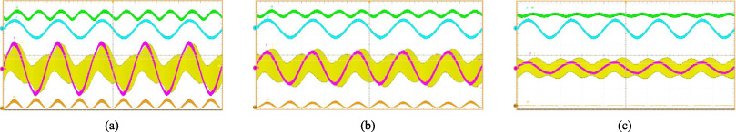
Main waveforms of the converter input and PFC stage delivering (a) 3.600 W, (b) 2.300 W and (c) 750 W: boost coil current, i b , (30 A/div, yellow), mains voltage, v ac , (400 V/div, blue), mains current, i f , (10 A/div, purple), bus voltage, v b , (400 V/div, green), and input power, p in , (10 kW/div, brown). Time: 10 ms/div.
The experimental results proving the proper operation of the converter are shown in Fig. 6 and Fig. 7 at different powers: 3.600 W in (a), 2.300 W in (b) and 750 W in (c), with a 400-V DC bus voltage. The main waveforms of the PFC stage are shown in Fig. 6, including the bus voltage, v b , the mains voltage, v ac , the boost coil current, i b , and the mains current, i f , whereas a zoomed detail of the load and PFC stage waveforms are shown in Fig. 7. The ZVS operation can be seen for both cases.
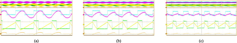
Detail of the main waveforms of the converter output and PFC stage delivering (a) 3.600 W, (b) 2.300 W and (c) 750 W: boost coil current, i b , (30 A/div, yellow), load voltage, vo,c, (400 V/div, blue), load current, i l , (30 A/div, purple), voltage between a and b half-bridges, vo,ab, (400 V/div, green), and output power, p out , (50 kW/div, brown). Time: 20 μs/div.
At maximum power, the converter is working at 20.5 kHz achieving a 92.5% efficiency. The EMC harmonic emissions for A-class devices are below the maximum limit. The achieved power factor is 99.7% while the current harmonic distortion, THDi, is 2.9%.
In this paper, a PFC front-end stage, its operation mode and its control strategy have been proposed to improve the flexible cooking surfaces. This stage allows controlling and increasing the bus voltage, easing the output power control and decreasing the power losses in the IH inverter due to the current through the IH load and inverter is lower.
The proposed operation mode and control strategy work with zero voltage switching (ZVS), decreasing the switching losses, enabling a higher working frequency and, therefore, decreasing the magnetic devices size. Besides, the switching frequency is constant in the mains cycle and can be modified to synchronize the load inverter and the PFC stage avoiding intermodulation noise. Finally, a 3.6 kW prototype has been implemented fulfilling EMC requirements and proving the feasibility of this proposal.
Footnotes
Acknowledgements
This work has been partially funded by the MINECO under the Project TEC2016-78358-R, by the Spanish MICINN and AEI under Project RTC-2017-5965-6, co-funded by EU through FEDER program, by the DGA-FSE, by the BSH Home Appliances Group, and by the Spanish MECD under the FPU grant FPU15/01590.