



Abstract
The contribution of this work is to propose miniaturized trisection bandpass filters (BPFs) using size-reduced substrate integrated coaxial resonators (SICRs). The applied SICRs are operated under a coaxial mode. The occupied circuit area of the SICR developed from its structurally similar one, the substrate integrated waveguide (SIW) cavity, is only 6.2% that of the latter, corresponding to a circuit-area reduction rate of 93.8%. The cross-coupling between the input and output resonators can be either a magnetic or electric coupling for locating the transmission zero near either the upper or lower passband edge, respectively. Sample trisection BPFs with magnetic/electric cross-couplings are built for experimental verification. Agreements between measured and simulated data are observed. These miniaturized trisection BPFs with a freely switchable transmission zero are endowed with the advantage of an excellent circuit-area efficiency in the category of SICR and SIW cavity trisection BPFs.
Keywords
Introduction
Bandpass filters (BPFs) designed using the trisection topology possess the advantage of an asymmetrical frequency response, which is very suitable for applications that require higher selectivity on only one side of the passband. These BPFs are usually composed of three resonators in a triangularly coupling form, in which a cross-coupling always exists between the input and output resonators. This cross-coupling may cause the filter to have a transmission zero (TZ) that can be located near the upper or lower passband edge, depending on the coupling mechanism [1, pp. 337–339]. This property is beneficial when designing a diplexer, in which the low-band (high-band) BPF can be designed to have a TZ around the central operating frequency of the high-band (low-band) BPF. Decades ago, trisection filters were mostly built of microstrip lines, which usually exhibit a low Q value. Recently, the substrate integrated waveguide (SIW) [2–6], an analogy to the metallic waveguide, brought us great attention for its numerous benefits, including lightweight, low profile, low cost, high Q value, good electromagnetic shielding, and high power-handling capacity. These SIWs are sometimes called post-wall waveguides [7] or, if consisting of multiple metal layers, laminated waveguides [8]. Undoubtedly, trisection BPFs formed by multiple SIW cavities have been progressively studied [9–12] because of the aforementioned advantages. In [10], the only TZ is created by the lower passband edge. In [10,11], the trisection BPF with a low-side TZ is cascaded with the BPF with a high-side TZ such that the resulting bandpass functions are sharp, although at the cost of high circuit complexity. In [12], the negatively frequency-dependent cross-coupling was first proposed in the SIW trisection filter design. However, the insertion loss (IL) is considered high, and the upper stopband bandwidth (BW) is too narrow.
Even worse, the SIW (or SIW cavity) was still criticized for its large footprint. This implied that the SIW was no match for its planar counterparts (e.g., the microstrip line, coplanar waveguide, and slotline), thus restraining its commercial applications. Several strategies have been reported to reduce the SIW size. The strategy of deforming the cross-section of the SIW resulted in half-mode [13] and folded half-mode [14] structures, which exhibit the circuit-area reduction rates of 50% and 75%, respectively. The other strategy was to lower the SIW’s operating frequency by loading itself with complementary split-ring resonators (CSRRs) [15,16], or slots [17–19]. In [20], an annular slot is created by etching the top wall of the square SIW cavity, allowing the capacitance to be established between the circular metal disk interior to the annular slot and the ground plane exterior to the annular slot. The circular disk is then connected to the bottom ground plane using a through via-hole. The embedded circular disk and the via-hole emulate the capacitance and the inductance effects, respectively, which together form an equivalent LC resonance circuit. Since the field distribution is more like that of a coaxial resonator, we should refer to the SIW cavity as the substrate integrated coaxial resonator (SICR). In such a prominent configuration, the SICR’s resonance frequency is lower than that of the standard SIW cavity (i.e., the SIW cavity without the extra embedded elements), leading to a circuit-size reduction rate of about 67%. Using the similar concept as that in [20], a novel vertical coaxial stepped-impedance resonator in a circular SIW cavity in [21] was built for a very compact trisection BPF, whose circuit-area reduction rate of the SICR reaches 97%. Clearly, the SICR proposed in [21] occupies a smaller circuit area than does the one presented in [20]. Although the structure in [20] with only one substrate layer, two metal layers, and through vias can be regarded as simple in structure, the capacitance formed by two edge-coupled plane conductors is small, and the inductance comes from the center via only. The resultant structural parameters that can be changed to adjust the resonance frequency are rather limited. In contrast, the structure in [21] is too complicated since three substrate layers, four metal layers, and via holes of through, buried, and blind types are all needed. Later in [22], a new square SICR whose structural complexity is between those of [20,21] was proposed. In [22], only two substrate layers, three metal layers, and vias of through and blind types are required to construct the square SICR. The capacitance required in the LC resonance can be large since it is formed by two broadside-coupled metal patches, and the inductance comes from either a center blind via or a circular array of vias. Many structural parameters can be employed to adjust the resonance frequency, and hence the design is flexible. The circuit-area reduction rate of this SICR is as large as 92.4%. To further reduce the circuit size, half-mode SICRs was employed to design BPFs of balanced types [23].
The SICR presented in [20] but with a circular cavity cross-section was later employed to cleverly construct a diplexer, whose two BPFs are of the trisection configuration [24]. The circuit performances of the trisection BPFs in [21,24] are both excellent. In [25], a new trisection BPF was realized using a single square SIW cavity that houses three resonators. Although more compact than those in [21,24], this new design is considered to be immature. This is because the three trisected patches each associated with a resonator impair the symmetry of the coaxial structure; hence empirical formulas for estimating the resonance frequency are not available. Furthermore, because both the input and output coaxial probes and the three shorting via-holes each associated with a resonator are all inside the same cavity, the magnetic couplings between resonators become very strong and very sensitive to manufacturing tolerance. Although the excessive magnetic couplings can be reduced by constructing a Y-shape slot in the cavity’s bottom wall, unwanted radiation leakage occurs.
For easier deployment of the trisection configuration in this paper, SICRs with a circular cavity instead of the square cavity employed in [22] are adopted. The circuit-area reduction rate of the circular SICR alone when compared with its unloaded counterpart (i.e., the circular SIW cavity without the circular patch and vias) is about 93.8%. The net cross-coupling between the input and output resonators can be either magnetic or electric for placing the TZ near either the upper or lower passband edge, respectively. Sample trisection BPFs of both net cross-couplings are fabricated for circuit verification. Measured results agree quite well with simulated ones. In addition, the nearest spurious band occurs far away from the desired frequency band with the upper stopband bandwidth larger than seven times the center frequency of the desired band.
Miniaturized SICR and sample trisection BPFs
Figure 1 shows the 3-D and side views of the proposed miniaturized SICR trisection BPF and the transmission line model of a single SICR unit. The two realizations of the proposed structure were outsourced to a professional PCB company for fabrication and packaging with good precision, and their dimensions will be presented later. In Fig. 1(c) the susceptance, B(ω), looking from the circular patch is expressed as

Proposed miniaturized SICR trisection BPF. (a) 3-D view, (b) side view, and (c) the transmission line model of a single size-reduced SICR unit.
Figure 2 gives the layouts and dimensions of the metal layers that comprise the BPF circuit. Two tightly stacked RT/Duroid 5880 substrates of thickness 0.254 (top substrate) and 1.57 mm (bottom substrate), dielectric constant (ϵ r ) 2.2, and loss tangent (tanδ) 0.0009 are used to build the filter’s SICRs. In this figure, the through vias forming the boundary of the circular cavity and the blind vias under the circular patch all have a diameter of 0.8 mm, the probe extended from the feeding coaxial cable has a diameter of 1.27 mm, and the circular aperture allowing the feeding probe to pass through has a diameter of 3 mm. The three circular cavities all have the diameter of 20 mm, and the center-to-center pitch between adjacent through vias on the cavity boundary is 2.61 mm. The smallest rectangle enclosing the circuit measures 39.6 × 37.4 mm2. Each circular cavity is loaded inside with a large capacitance formed by the embedded circular patch and the cavity’s top and bottom walls. The patch is also shorted to the cavity bottom wall by the blind vias that form a hollow cylinder (shown in Fig. 2(b)), which provides a loaded inductance. As a result, the cavity resonates at a coaxial mode whose frequency is much lower than the resonance frequency, f 0, of the circular cavity’s dominant TM010 mode.
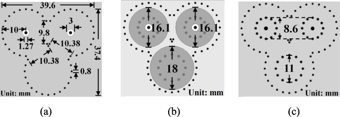
Layouts of the composing cavities with circuit dimensions (in mm) for the BPF in Fig. 1. (a) Top metal layer, (b) middle layer, (c) bottom layer.
Shown in Fig. 3 are the normalized resonance frequency f
r
∕f
0 and the unloaded Q
u
vs. the diameter, D, of the embedded patch and the diameter, R, of the circle constituted by the shorting via-ring. Here, f
0 = 7.74 GHz is the TM010 resonance frequency of the unloaded circular SIW cavity (i.e., the circular SIW cavity without embedded metals inside). The bigger patch (i.e, a larger value of D) and a smaller diameter of the via-ring circle (i.e., a smaller value of R) provide a larger capacitance and a smaller Y
0, respectively, hence leading to a lower f
r
. Equivalently, the smaller f
r
denotes a larger circuit size reduction. This resonance can also be regarded as an LC resonance with the capacitance and inductance given by C
d
= πϵ
r
ϵ0 D
2(1∕h
1 +1∕h
2)∕4 (see Fig. 1(b)) and L = μ0 h
2 ln(R
C
∕R)∕(2π), respectively, where ϵ0 and μ0 are the permittivity and permeability of vacuum, respectively. From the expression of the inductance L, it is of no surprise that, in Fig. 3, a smaller value of R corresponds to a smaller f
r
. It can be verified that the resonance-frequency formula
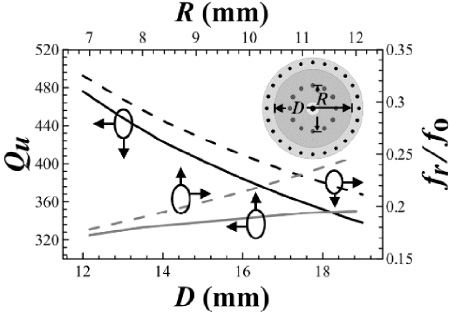
Curves of the normalized resonance frequency, f r ∕f 0, and Q u vs. the patch diameter, D, and via-ring diameter, R.
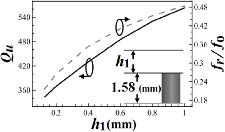
Curves of the normalized resonance frequency, f r ∕f 0, and Q u vs. the top substrate thickness, h 1.
In Fig. 5, we give the measured and simulated frequency responses for the proposed trisection BPF in Fig. 1. To design the filter, the coupling matrix synthesis (CMS) method is applied to obtain the required coupling coefficients between the three resonators in the BPF, and the commercial simulation tool HFSS [26] is then used to approach all the circuit dimensions given in Fig. 2. Note that the couplings between three resonators are all magnetic, as evidenced from the positive values in the CMS matrix. For example, the CMS matrix elements M 12 and M 13 in Fig. 5(b) have the values of 0.9285 and 0.5241, respectively, which are associated with the couplings provided by the open windows between cavity pair (1, 2) and cavity pair (1, 3). Obviously, the coupling window of the former (with the width of 10.38 mm in Fig. 2(a)) must be larger than that (the width of 9.8 mm) of the latter, since the former requires a stronger coupling. The measured (simulated) passband central frequency is 1.86 (1.85) GHz with the measured (simulated) minimum IL and fractional bandwidth (FBW) of 1.7 (0.92) dB and 6.71% (7.6%), respectively. Note that the simulated resonance frequency of 1.85 GHz against that (7.74 GHz) of the unloaded SIW cavity indicates that the circuit-area reduction rate of the SICR is about 94.3%. From Fig. 5(a), we note that the out-of-band −20 dB transmission coefficient occurs at a frequency that is much larger than the displayed upper frequency limit of 16 GHz. This implies that the measured upper stopband BW is much wider than 7.5f r under the condition of signal rejection level greater than 20 dB, where f r . is the center frequency of the measured operating band. Also note that the nature of the trisection filter design is to possess a TZ, as is evidenced in Fig. 5(a). This TZ can be shifted to the passband’s low-end edge if the coupling between the input and output resonators is switched from magnetic coupling to electrical coupling.
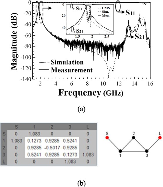
The frequency responses for the proposed BPF in Fig. 2. (a) Measured and simulated frequency responses, (b) CMS matrix and circuit’s trisection topology.
In Fig. 6, we give the layouts of the trisection BPF with a negative coupling between resonators 1 and 3. In this figure, the through vias on the cavity boundary, blind vias under the circular patch, feeding structure, and diameter of the circular cavity all have the same dimensions as those in Fig. 2. The smallest rectangle enclosing the circuit measures 40.8 × 38.5 mm2. From the CMS simulation, the passband’s upper-edge TZ can be shifted to the lower passband edge while the coupling mechanism between resonators 1 and 3 is switched from magnetic coupling to electric coupling. Here, the former is termed positive coupling and the latter is called negative coupling. As shown in Fig. 6(b), the negative coupling structure is implemented by two rectangular-ring slots laid over the patches. The 1-mm-diameter through via between the two rectangular-ring slots helps decouple the two slots.

Layouts and the circuit dimensions (in mm) of the trisection BPF with negative coupling structure. (a) Top metal layer, (b) zoom-in of negative coupling structure, (c) middle layer, and (d) bottom layer.
Figure 7 shows the curve of the coupling coefficient vs. the slot width w. As a fact, the coupling structure in Fig. 6(b) has the combined effect of the magnetic and electric couplings with the former caused by the coupling window between the cavities and the latter arising from the rectangular-ring slots that provide the cavities with an electric coupling. The overall coupling effect becomes an electric coupling while the electric coupling exceeds the magnetic one. In such a case, the rectangular-ring slots with a larger width (w) are preferred for a negative coupling design, and this negative coupling gives the trisection filter a transmission zero by the passband’s low-end edge.
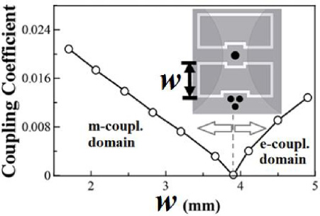
Coupling coefficient vs. the slot width w.
Figure 8 shows the measured and simulated frequency responses for the trisection BPF proposed in Fig. 6. It is evidenced from Fig. 5(a) and Fig. 8 that the TZ is shifted from the upper passband edge (Fig. 5(a)) to the lower passband edge (Fig. 8) while the coupling between resonators 1 and 3 is switched from positive to negative. An additional TZ around 1.5 GHz in Fig. 8 is believed to be caused by the cross-coupling between the input and output feeds. The measured (simulated) passband central frequency is 1.92 (1.93) GHz with the measured (simulated) minimum IL and FBW of 1.8 (0.64) dB and 6.8% (7.9%), respectively. From the simulated resonance frequency of 1.93 GHz, it can be concluded that the circuit-area reduction rate of the SICR is about 93.8%. The measured upper stopband limit shown in Fig. 8 extends beyond the displayed frequency scope of 16 GHz. The photos of the experimental circuits for both the positive and negative coupling sample BPFs are given in Fig. 9. For convenience, important circuit-performance parameters of our designs are summarized in Table 1, in which those of related SICR and SIW cavity trisection BPFs are also shown for comparison. In this table, the circuit size denotes the width and length of the smallest rectangle that can enclose all the cavities of the trisection BPF with the feeding microstrip lines excluded. Obviously, the BPF in [25] is the most compact one. This is partially because the rectangle we just mentioned coincides with the square cavity’s cross-section in [25]. In contrast, for our trisection BPFs, this rectangle also encloses some area that is exterior to the three circular cavities. Nevertheless, the measured circuit performances of the two SICR trisection BPFs presented here are comparable with others in the table. In particular, our BPFs exhibit the largest upper stopband bandwidths.

Measured and simulated frequency responses for the BPF in Fig. 6.
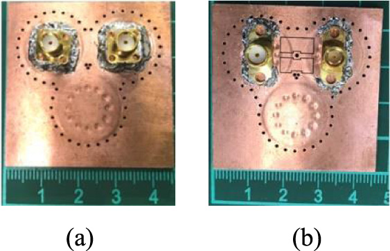
Photos of the experimental circuits. (a) Positive coupling and (b) negative coupling designs.
Comparison of measured performances of our designs and related SICR and SIW cavity trisection BPFs
𝜆 d : the intrinsic wavelength in the dielectric media at the frequency f r ; USBW: abbreviation for upper stopband BW.
Design, realization, and verification of the miniaturized SICR trisection BPF have been presented in this paper. Magnetic and electric cross-couplings are successfully applied to the trisection BPF design for placing the transmission zero near the upper and lower passband edges, respectively, without increasing the circuit complexity and circuit area. Good agreement between the measurement and the simulation is observed. With an occupied circuit area of only 0.36𝜆 d × 0.4𝜆 d , the proposed SICR trisection BPF has achieved an excellent circuit-area efficiency among the categories of the SICR and SIW cavity trisection BPF. In this design, the dimensions of the proposed circuit can be properly scaled up or down to cope with a real application whose operating bands are different from the one achieved in this article.
Footnotes
Acknowledgements
This work is supported by the Ministry of Science & Technology, R. O. C. under grant contracts MOST 109-2221-E-018-018 and MOST 110-2221-E-018-005.