To investigate portable, low power consumption, low cost and green high-performance computing (HPC) technologies which are suitable for industry applications, authors have been working on the development of dedicated computer based on dataflow architecture for electromagnetic field simulations. In this paper, we propose a Finite Integration Technique (FIT) dataflow machine based on BiCG-Stab scheme for 3-D electrostatic field simulations.
The high-performance computing (HPC) technologies have been developing until now, and the peak performance of the latest supercomputer has reached to 1680 pflop/s. However, such the supercomputers are extremely huge system, which consist of over 8 million cores and need 20 MW power consumption. This means that such the HPC technologies are not suitable for product design in industry. We have been working on the development of a dedicated computer to aim to achieve a portable, low cost, low power consumption and green HPC to be used for industry applications [1–4]. In previous works, we proposed a dedicated computer for 2-D magneto-static field simulations [5–7], in which we designed hardware circuit of the BiCG-Stab matrix solver based on dataflow architecture to execute the finite integration technique (FIT) scheme in 2-D grids space. In addition, we proposed a dedicated computer for microwave simulations [8–16], in which we discussed a hardware circuits of finite-difference time-domain (FDTD) scheme based on sliced 3-D dataflow architecture for 3-D grids space. In this paper, we consider to design a 3-D FIT dataflow machine for electrostatic field simulations combing techniques of the BiCG-Stab scheme circuits and sliced 3-D grid dataflow architecture in previous works.
FIT scheme for 3-D electrostatic field simulation
In order to achieve high performance dedicated computer for the 3-D electrostatic fields, the use of FIT scheme is crucial to achieve highly parallel computation based on dataflow architecture. We here summarize an overview of the FIT scheme for 3-D electrostatic field simulation.
In the FIT scheme for 3-D electrostatic field simulation, the following integral form of Gauss’s law is discretized in 3-D grids space, where 𝜌 is the charge density, 𝜙 is the scalar potential and ϵ is permittivity. As shown in Fig. 1, If we allocate the component of the scalar potential 𝜙 at i-th, j-th, k-th grid in all 3-D grids space, ((1)) can be expressed in discretized form as follows: where,
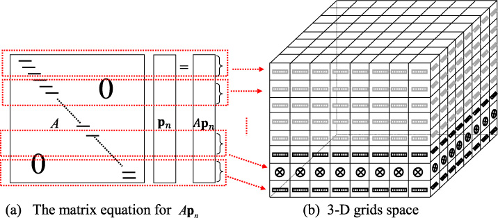
To obtain the distribution of the electrostatic potential 𝜙, which satisfy the FIT discretization (2) for all 3-D grids space simultaneously, we need to construct the FIT matrix equation as shown in Fig. 2 and solve the FIT matrix equation. Then, the boundary condition is taken to be 0 at the outer boundary which is sufficiently far away from the field source.
Hardware circuit of BiCG-Stab matrix solver based on dataflow architecture
For the FIT matrix equation (Fig. 2), we here consider to use the BiCG-Stab scheme which is a relatively stable matrix solver. The detail procedure of the BiCG-Stab scheme for a matrix equation Ax = b is as follows:
1. Set an initial value x0
2. Compute initial residual r0 = b − Ax0
3. Set the shadow residual vector r0∗ s.t. (r0, r0∗) ≠ 0, e.g., r0∗ = r0
4. Set 𝛽−1 = 0, then the search direction vector p0 = r0
5. For n = 0, 1, 2, …, until (ϵ = 10−9)
begin end
In the BiCG-Stab scheme, before the iteration process (i)–(vii) starts, the appropriate initial values x0 and initial residual r0 are set. Then, the iteration process (i)–(vii) of the BiCG-Stab are repeated until the residual rn satisfies convergence condition (ϵ = 10−6 ∼ 10−9). The unit grid circuit of FIT dataflow machine for 3-D electrostatic fields simulation based on BiCG-Stab scheme is designed as shown in Fig. 3. All of unkown values of (pn, Apn, tn, Atn, xn, rn) in the iteration process of the BiCG-Stab and the coefficient values of of ((2)) are stored in the registers of each grids, and these registers are connected each other by arithmetic circuits to execute the iteration process (i)–(vii) in ((4)) of the BiCG-Stab scheme. For example, the circuit connection of pn of the BiCG-Stab iteration process of (vii) in ((4)) is highlighted as shown in Fig. 3, and the logic circuit of other steps of BiCG-Stab iteration process can be implemented as same as the circuit of pn in Fig. 3. In addition, Fig. 3 includes circuits for one row of matrix-vector multiplications Apn and Atn in the BiCG-Stab iteration process (i) and (iii). If the unit grid circuits of Fig. 3 are connected all over 3-D grids space, inner product calculation of (i) and (iii) in ((4)) can be executed in single clock cycle, which is the extremely high-performance computation. However, such 3-D grid circuits will result in a very large size hardware, and it is impossible to be implemented in a single LSI (Large-Scale Integrated Circuits).
Unit grid circuit of BiCG-Stab matrix solver.
Sliced 3-D dataflow architecture for BiCG-Stab scheme
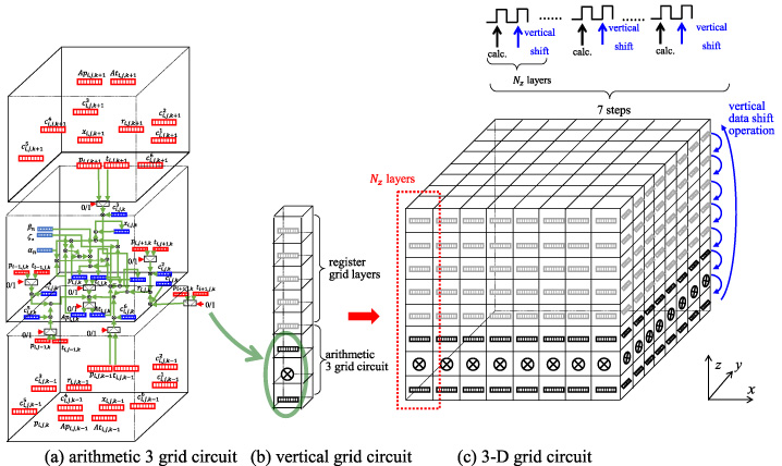
In this work, we consider to use sliced 3-D dataflow architecture, which was used in 3-D FDTD dataflow machine, for implementation of the 3-D dataflow architecture machine in practical hardware size. Figure 4(a) depicts three grid circuits which consist of arithmetic grid circuits of Fig. 3 at the middle and additional two register grid circuits. The upper and lower grid circuits (register grid circuit) contain only registers for storing unknown values (pn, Apn, tn, Atn, xn, rn) of the BiCG-Stab iteration process and coefficient values of (2). We here called these circuit “arithmetic 3 grid circuit”. In Fig. 4(b), additional register grid circuits (which are same as the upper or lower grid circuit in Fig. 4(a)) are connected vertically upon the arithmetic 3 grid circuit. To connect the vertical grid circuit of Fig. 4(b) horizontally, 3-D grid circuit is constructed as in Fig. 4(c). Then, in the 3-D grid circuit of Fig. 4(c), after execution of calculation of (4) for the bottom layer register values, it is necessary to exchange register values by the upper layer register values to do shift-down operation. That is, to repeated the execution of (4) at the bottom layer and shift-down operations, the calculation of (4) can be executed for all 3-D grids. It is known that hot-spot parts of the BiCG-Stab scheme are calculations of the matrix-vector multiplications of Apn and Atn in (i) and (iii) of (4). In the 3-D grid circuits for the FIT scheme, a part of calculations of the Apn for one layer can be executed in a single clock cycle as shown Fig. 5. If we denote the number of layers of 3-D grid circuits of Fig. 4(c) as Nz, the calculation of Apn can be done only by 2Nz clock cycles including vertical shift operations.
Sliced 3-D dataflow architecture.
The matrix equation corresponds to 3-D grids space.
The whole configuration of FIT dataflow machine.
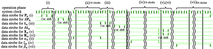
VHDL simulation for MASTER SCHEDULER.
VHDL simulation result for one columon of 3-D grids space.
Configuration of FIT dataflow machine for 3-D electrostatic field simulation
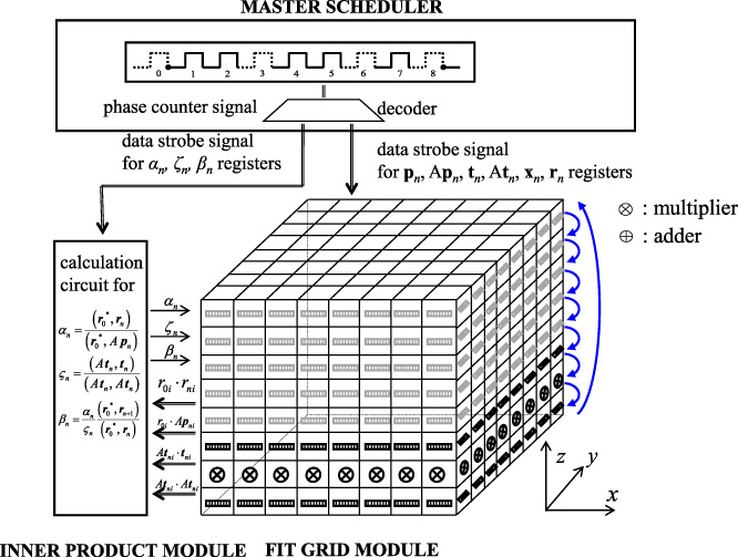
In this section, we construct entire structure of the FIT dataflow machine for 3-D electrostatic field simulation to use the 3-D grid circuit of Fig. 4(c), and described the machine operation in particular for execution of the BiCG-Stab matrix calculation. The whole configuration of 3-D FIT dataflow machine consists of 3 parts as shown in Fig. 6, MASTER SCHEDULER, INNER PRODUCT MODULE, and FIT GRID MODULE. The FIT GRID MODULE executes the BiCG-Stab iteration process (i)–(vii) as mentioned in the previous section. The INNER PRODUCT MODULE collects the multiplications of r0i, j, kri, j, k, r0i, j, kApi, j, k, ti, j, kAti, j, k, Ati, j, kAti, j, k from the FIT GRID MODULE, and inner product calculations of 𝛼n, 𝜍n, 𝛽n are executed to be sent back to the FIT GRID MODULE. These two modules are controlled by the data strobe (DS) signals from the MASTER SCHEDULER. The circuits of the dedicated computer is designed by a hardware description language VHDL. A VHDL logic circuit simulation of MASTER SCHEDULER for single iteration process of the BiCG-Stab scheme of (4) is depicted in Fig. 7. For each calculations of (ii), (iv), (v), (vii), arithmetic calculation at the bottom layer and vertical shift operation are carried out all over the 3-D grids. Accordingly, the single BiCG-Stab iteration process for all 3-D grids space takes (2Nz × 5 + 3Nz + 48) clock cycles.
Numerical example
In Fig. 8, an example of the VHDL logic circuit simulation for the pn of (vii) in (4) in the vertical grid circuit (Fig. 4(b)) is indicated. When the DS signals for pn is high-level, the value of pn in the computation layer is updated. On the other hand, when the DS signals for pn is low-level, the unkown values (pn, Apn, tn, Atn, xn, rn) of the BiCG-Stab iteration process and coefficients value of each layer are shifted-down to the lower layer. We confirm that the calculation of pn is performed normally according to the scheme of (vii) in (4), which means that the VHDL design of the part of the vertical grid circuit in the sliced 3-D dataflow machine is carried out correctly.
Conclusion
In this paper, we have presented the design of the FIT dataflow machine for 3-D electrostatic fields simulations. The detailed logic circuits of sliced 3-D dataflow architecture for the BiCG-Stab scheme is proposed, and a whole configuration for 3-D electrostatic fields FIT dataflow machine is discussed. The logic circuit of the vertical grid circuit of 3-D FIT dataflow architecture machine was designed by the VHDL and it was confirmed by the VHDL circuit simulation that the logic circuits for the BiCG-Stab scheme are implemented correctly. We will proceed to the VHDL logic circuit simulation for the whole 3-D FIT dataflow machine of electrostatic field simulation in near future.
References
1.
PlacidiP.VerducciL.MatrellaG.RoselliL. and CiampoliniP., A custom VLSI architecture for the solution of FDTD equations, IEICE Trans. Electron.E85-C(3) (2002), 572–577.
2.
SanoK.HatsudaY.WangL. and YamamotoS., Performance evaluation of Finite-Difference Time-Domain (FDTD) computation accelerated by FPGA-based custom computing machine, Interdisciplinary Information Sciences15(1) (2009), 67–78.
3.
FujitaY. and KawaguchiH., Development of improved memory architecture FDTD/FIT dedicated computer based on SDRAM for large scale microwave simulation, International Journal of Applied Electromagnetics and Mechanics32(3) (2010), 145–157.
4.
KawaguchiH.TakaharaK. and YamauchiD., Design study of ultra-high speed microwave simulator engine, IEEE Transactions on Magnetics38(2) (2002), 689–692.
5.
WangC.X.OtaS. and KawaguchiH., Conceptual design of dataflow machine for magnetostatic field simulation, in: Proceedings of the 2021 International Conference on Electromagnetics in Advanced Applications (ICEAA), Hawaii, USA, 2021, p. 223, ID:694.
6.
WangC.X. and KawaguchiH., Design study of BiCG-Stab matrix solver circuit for FIT scheme based on dataflow architecture, in: Proceedings of the International Conference on Simulation Technology (JSST 2021), Kyoto, Japan, 2021, pp. 402–403.
7.
WangC.KawaguchiH. and WatanabeK., Study of FIT dedicated computer with dataflow architecture for high performance 2-D magneto-static field simulation, IEICE Trans. Electron.E106-C(4) (2023), to be published.
8.
KawaguchiH.FujitaY.FujishimaY. and MatsuokaS., Improved, architecture of FDTD/FIT dedicated computer for higher performance, computation, IEEE Transactions on Magnetics44(6) (2008), 1226–1229.
9.
FujitaY. and KawaguchiH., Full custom PCB implementation of FDTD/FIT dedicated computer, IEEE Transactions on Magnetics45(3) (2009), 1100–1103.
10.
FujitaY. and KawaguchiH., Development of improved memory architecture FDTD/FIT dedicated computer based on SDRAM for large scale microwave simulation, International Journal of Applied Electromagnetics and Mechanics32(3) (2010), 145–157.
11.
FujitaY. and KawaguchiH., Development of portable high performance computing system by parallel FDTD dedicated computers, in: 18th International Conference on the Computation of Electromagnetic Fields, 2011.
12.
MatsuokaS.OhmiK. and KawaguchiH., Study of a microwave simulation dedicated computer, FDTD/FIT data flow machine, IEICE Trans. Electron.,E86-C(11) (2003), 2199–2206.
13.
KawaguchiH. and MatsuokaS., Conceptual design of 3D FDTD dedicated computer with dataflow architecture for high performance microwave simulation, IEEE Tran. Magn.51(3) (2015), 7202404.
14.
KawaguchiH., Improved architecture of FDTD dataflow machine for higher performance electromagnetic wave simulation, IEEE Tran. Magn.52(3) (2016), 7206604.
15.
KawaguchiH. and MatsuokaS., Implementation of microwave simulation at dispersive material in dataflow architecture FDTD dedicated computer, IEEE Tran. Magn.54(3) (2018), 7202205.
16.
KawaguchiH., Design study of domain decomposition operation in dataflow architecture FDTD/FIT dedicated computer, IEICE Trans. Electron.E101-C(1) (2018), 20–25.