
Abstract
Remarkable progress has been made to understand the chemical vapor deposition (CVD) of two-dimensional (2D) materials over the last two decades. The review summarized the state-of-the-art experimental synthesis and modelling and simulation on 2D materials CVD growth. Firstly, the family of 2D materials, and their CVD growth processes are introduced. Secondly, the experimental synthesis and modelling and simulation on graphene growth are discussed. In particular, the applications of reactive molecular dynamics methods, kinetic Monte Carlo and density-functional theory in 2D material growth are addressed. Then, the CVD growth of hexagonal boron nitride and transition metal dichalcogenides are further discussed, focusing on the effects of reaction conditions (growth temperature, pressure, vapour-phase composition, etc.) on the domain morphologies, edge structures and grain boundaries of 2D materials. Last, conclusions and outlooks are presented.
Introduction
Family of 2D materials
The door for two-dimensional (2D) materials has been opened since graphene was first mechanically exfoliated in 2004 [1]. As a result, increasing number of 2D materials have been obtained by mechanical/liquid exfoliation and chemical vapour deposition. Their unique structures, excellent properties, and potential applications have been investigated experimentally and theoretically [2, 3, 4]. These studies have demonstrated many excellent properties and demonstrated diverse potential applications of 2D materials, in electronics/optoelectronics [5, 6, 7], sensor [8, 9, 10, 11], energy storage [12, 13, 14], surface catalysis [15, 16], biology [17, 18], etc. Besides graphene consisted of C element, there exist other elemental 2D materials of Group IV (Si, Ge, Sn) elements, such as silicone [5, 19, 20], germanene [21, 22, 23, 24, 25], and stanene [25, 26, 27, 28, 29, 30]. Interestingly, these Group-IV-elemental 2D materials exhibit a slightly-buckled structure, which is different from the planar graphene.
Semiconducting Group-V-elemental 2D materials, for example phosphorene [31, 32, 33], arsenene [3, 34], and antimonene [3, 34, 35, 36, 37, 38], except these Group-IV-elemental 2D materials, have also attracted large amount of attentions. For example, phosphorene is appropriate for high-speed optoelectronics and nanoelectronics because it is a direct bandgap semiconductor having a high on/off ratio and an extreme-high carrier mobility [39, 40]. Furthermore, borophene consisted of monolayer boron atoms is a metallic 2D elemental material. Although borophene has some similar free energies phases [41, 42], appropriate substrates could be relatively stable [43, 44, 45].
In addition to elemental 2D materials, compound 2D materials are also of great interest. Morphologically alike to the honeycomb graphene and even with quite similar bond length. Instead of 2.46 Å in C, lattice parameter in hexagonal boron nitride (hBN) is 2.51 Å. The chemical alternation of B and N atoms causes the ionic nature of this distinctly different, insulating crystal [46].
The most popular synthetic 2D materials are transition metal dichalcogenides (TMDs) [4, 47], which are a group of semiconductors with 10
Chemical vapor deposition
Chemical vapor deposition (CVD) is capable to produce large-area 2D materials [54], which has been employed to grow graphene [55, 56], TMDs [57, 58, 59], and hexagonal boron nitride (hBN) [60, 61]. Among TMDs, the representative materials obtained by CVD are MoS
Atmospheric-pressure CVD growth is commonly employed [66, 67, 68], however, researchers have also utilized low-pressure or even vacuum CVD growth of 2D materials [69, 70, 71], using a vacuum pump to maintain the low pressure. On account of whether the vapor-phase precursors are generated inside the reactor or enter the reactor, CVD growth of 2D materials can be categorized into two types: gas-phase precursors get into the reactor (type 1), for example, hydrogen and methane gas for graphene, H
The CVD growth of 2D material involves competing and auxiliary atomistic processes [72], including diffusion/desorption/adsorption of precursors to/from/on the substrate surface, reactants vapor-phase transportation and nucleation of the 2D material, growth/etching of the 2D material involving detachment and attachment of adatoms, the diffusion along the edge of the 2D material [73]. These processes are depicted in Fig. 1. The growth is highly dependent based on the kinetics and energetics during multiplex processes. Theory or model that can be used to make prediction is of great importance. Actually, if the nucleation of another domain is harder/slower than the lateral growth of the 2D material, then large-scale single-crystal growth will occur. Otherwise, island-type growth will take place, leading to the polycrystalline growth.
Atomistic processes during the growth of 2D materials. 
Experimental synthesis
Graphene is the first 2D synthesized material, which has been widely used in many application areas, e.g., water desalination [74], gas separations [75], electronics [76, 77], energy storage [78, 79], and biosensing [80]. Graphene was initially synthesized using mechanical cleavage [81], however, this method is not scalable and results in quantities of small-sized 2D flakes. Therefore, researchers have turned into other techniques to produce large-scale graphene, such as top-down liquid exfoliation [82]. However, liquid-exfoliated graphene’s lateral size is also limited and has some defects because of the vigorous conditions presented by ultrasonication [83].
To overcome these challenges, researchers have developed bottom-up CVD, which can help graphene grow potentially. Multi-layered graphene, was first synthesized via CVD in 2007 [84]. Subsequently, single-layered graphene was further synthesized via CVD in 2008 to 2010 [85, 86, 87]. The CVD growth of graphene utilizes methane and hydrogen gases as reactants. Through theoretical and experimental methods,we understand the mechanism of growth on various substrates and graphene nucleation [88, 89, 90]. For example, Tetlow et al. extensively reviewed the research progress in the growth of graphene [88]. In terms of experimental studies, Girit et al. studied the graphene mechanism of edge reconstruction, by aberration-corrected transmission electron microscopy [89]. Later, Bhaviripudi et al. experimentally researched the importance of the reactor pressure in the growth kinetics of graphene on Cu substrate.
Vlassiouk et al. showed that graphene CVD growth on copper foil using methane as a carbon source is strongly affected by hydrogen [91]. Hydrogen appeared to serve a dual role: an activator of the surface bound carbon that was necessary for monolayer growth and an etching reagent that controlled the size and morphology of the graphene domains. Luo et al. demonstrated that through the rational design of low-pressure CVD of graphene in hydrogen-diluted methane and regulation of the flow rate of H
Control of the stacking angle of bilayer graphene is essential for fundamental studies and applications. Cho et al. observed the rotation of graphene during CVD through experimental results combined with theoretical calculation [93]. The rotation can be blocked or accelerated by controlling the growth temperature, by which highly selective growth of AB-stacked bilayer graphene or 30
Modelling and simulation
On the modelling and simulation, Artyukov and Yakobson performed detailed density-functional theory (DFT) calculations on the graphene edges growth rate, using a step-flow model of crystal growth [90]. The authors simulated the carbon migrating adatoms from the feed, to the Ni substrate surface and their attachment to the growth front. Afterwards, they computed many intermediate states energies, to clarify the sequence of steps in the growth of graphene process. The adatoms were attached to the graphene edges, and hardly form defects in the substrates presence. This work provides good evidence on anisotropic growth process, the complex growth kinetic, and the diverse domain morphologies, thus providing insights into the experimental growth.
Meng et al. investigated the growth kinetics of carbon structures on Ni (111), using reactive molecular dynamics (MD) simulations at various temperature with the ReaxFF potential [95]. This study indicated that higher carbon atoms concentrations, advantageous to form graphene island and lower carbon concentrations cause carbon dissolution into the Ni surface. Thus, continuous growth of single domain are not feasible at a high concentration because of the graphene islands formation, nor at low carbon concentration, for the growth precursors, advising an appropriate carbon concentration can make large-area growth.
Researchers also studied the non-linear graphene growth mechanism using DFT calculations and kinetic Monte Carlo (kMC) simulations on metal surfaces. For example, Wu et al. modelled the supply, diffusion, adsorption of smaller carbon species.(as shown in Fig. 2) Through studying the step sites on the substrate, and attachment of carbon adatoms to the graphene edges, they clarified the mechanism of growth and nucleation [96]. The lattice mis-match between the growth substrate and graphene lead to uneven growth.
KMC model on the graphene growth. (a) kMC model Schematic diagram: standing on the front of graphene growth. (b) Graphene growth rates dependent on C monomer concentration, which obtained by kMC simulations. Reproduced with permission [96].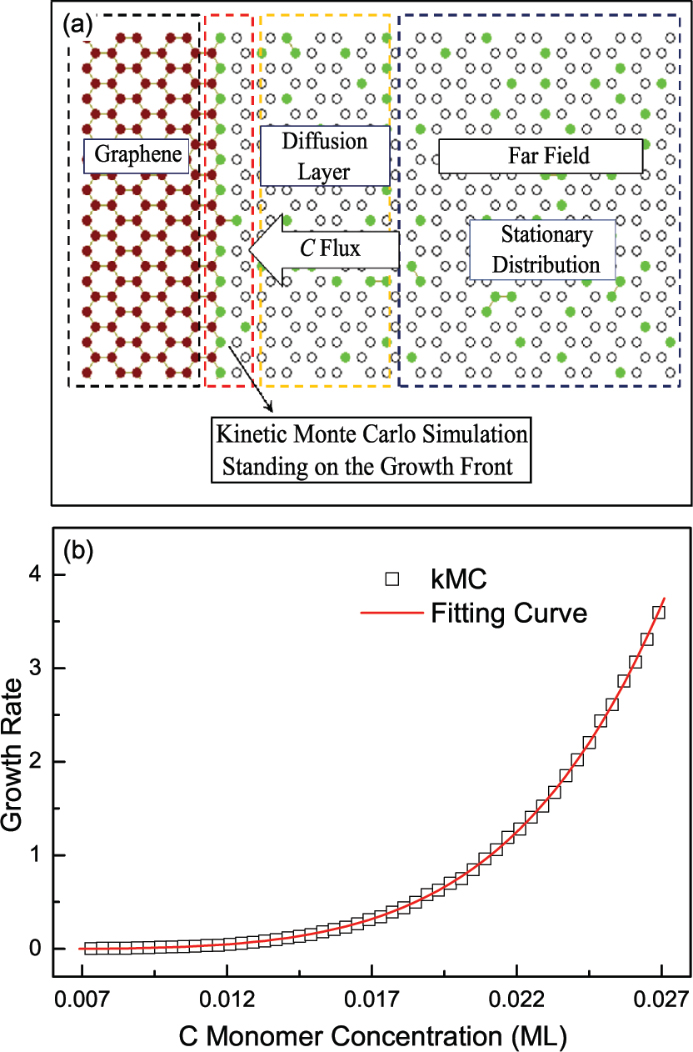
Meca et al. formulated a phase-field model that explicitly accounted for the anisotropies in the energies of growing graphene edges, kinetics of attachment of carbon at the edges, and the crystallinity of the underlying copper substrate (through anisotropy in surface diffusion) [97]. They showed that anisotropic diffusion has a very important, counterintuitive role in the determination of the shape of islands, and present a “phase diagram” of growth shapes as a function of growth rate for different copper facets.
Research efforts to evaluate the theoretical methods accuracy are also crucial to ensure that modelling and simulation predictions are reliable. For example, Shu et al. studied the formation of carbon species using DFT calculations during the CVD growth of graphene [98]. They revealed that both C and CH monomers are dominant on the Cu substrate. On Ni substrate, during graphene growth the number of C monomer is large. C species were stable on Ir and Rh surfaces, driving their CVD growth process. Simulation studies considering the effect of temperature on growth are also essential to understand the graphene growth. In DFT calculations, thermal effects are included in the harmonic oscillator approximation [99].
Experimental synthesis
HBN, is an insulating 2D material, has potential applications in optoelectronic devices,also known as white graphene [100, 101], molecular/ionic separations [102, 103], and osmotic power harvesting [104, 105]. Allendorf et al. investigated the CVD growth kinetics of BN, from BCl
Song et al. studied the thermodynamics and kinetics during the CVD growth of hBN, from solid ammonia borane [109]. The effect of flow rate of carrier gas, growth time, and growth temperature were systematically investigated. Remarkably, the researchers had the ability to manufacture large-scale (80 mm
Tian et al. proposed an in situ CVD growth strategy for synthesizing wafer-scale AAB-stacked single-crystal graphene/hBN/graphene trilayer van der Waals heterostructures [111]. Single-crystal CuNi(111) alloys were prepared on sapphire, followed by the pre-dissolution of carbon atoms. Single-crystal monolayer hBN was synthesized on a plasma-cleaned CuNi(111) surface. Then, a single-crystal monolayer graphene was epitaxially grown onto the hBN surface to form graphene/hBN bilayer heterostructures. A controlled decrease in the growth temperature allowed the carbon atoms to precipitate out of the CuNi(111) alloy to form single-crystal graphene at the interface between hBN and CuNi(111), thereby producing graphene/hBN/graphene trilayer van der Waals heterostructures.
Modelling and simulation
In terms of modelling and simulation, Yakobson et al. first calculated the edge energies of BN and considered both N-rich and B-rich zigzag edges [46], as shown in Fig. 3. The B and N atoms edge energies have been reported, one of edge energies, providing insights on how to control the morphology of hBN domains and determine the resultant properties of BN. A method which at a special chemical potential can evaluate edge energy in any crystallographic direction has been developed. Besides, the Wulff construction method has been applied to predict the balanced forms of a variety of BN clusters, indicating that the balanced BN domains to be triangular, the edges are jagged.
Geometries and energies of BN structures showed above: boron atoms (red circle) and nitrogen (blue circle). (a) Ribbon like armchair. (b) Zigzag ribbon. (c) B-rich triangle. (d) N-rich triangle. (e) Total energy as a function of their size 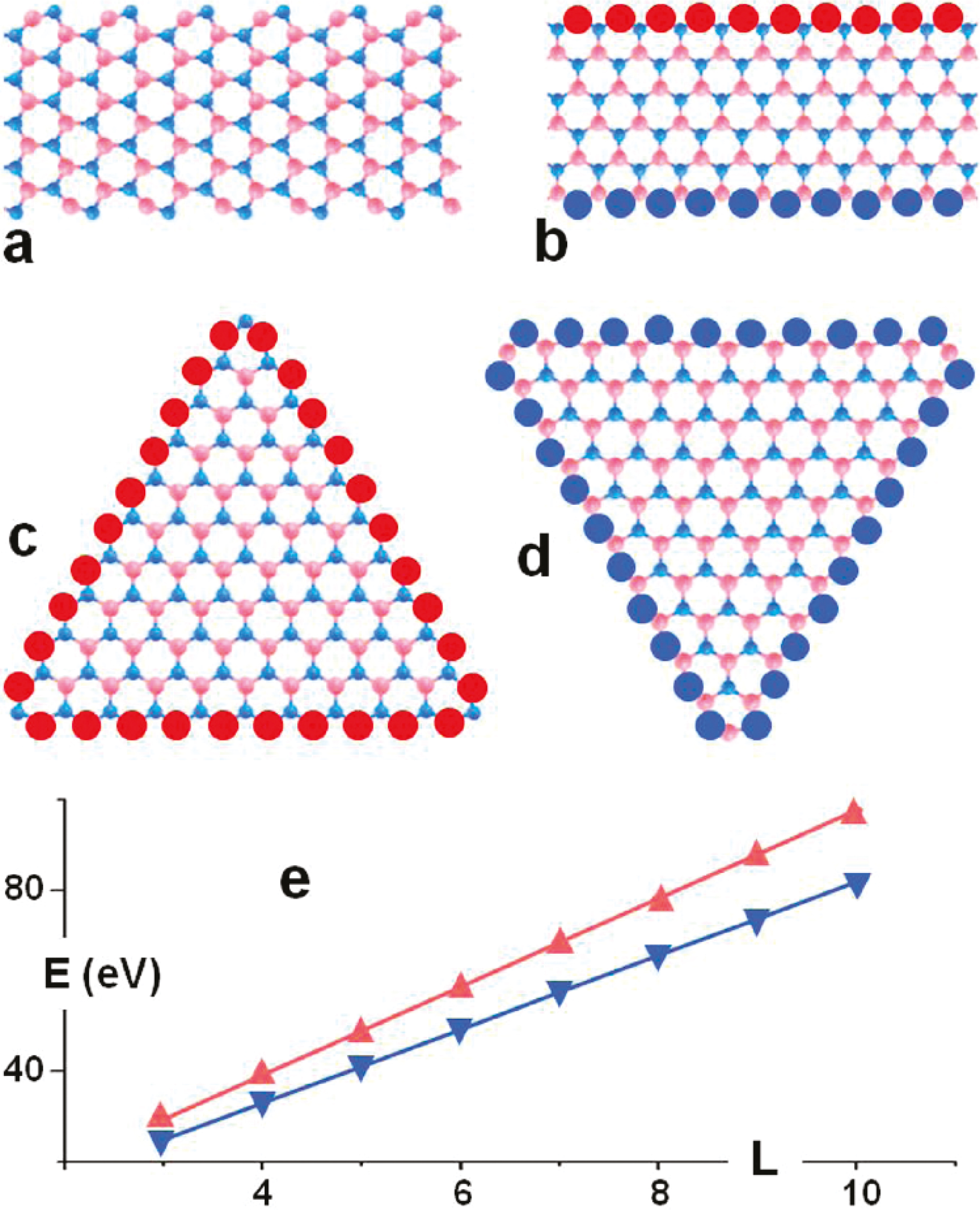
In another work, Liu et al. studied the aline of monolayer hBN on the surfaces of Cu (100) using DFT method [112]. At the initial nucleation stages, total energy calculations and rotational angles, revealed the origin that hBN grew on the surface, in a specific orientation. In the future, investigations on the rotation obstacle could further unveil the rotational directions stability in experimentally-observed structures during CVD growth in more detail. Furthermore, rearrangements of Cu atoms in the lattice were observed, as a result of the Cu substrate and the B/N atoms bonding interactions, thus indicating the effect of non-van der Waal interactions on the domain orientations.
Ding et al. investigated the hBN CVD growth on various substrate (Rh (111), Cu (111), and Ni (111)) [113]. The results indicated that hexagonal domains were energetically favorable than other domain shapes, e.g., heptagons or pentagons. Furthermore, the serrated edge was better than the chair edge for hBN. Calculations of the edge interactions with the bottom metal placode further indicated that the edges winding to the substrate, leading to electric charge shift around them. In the way of Klein edges, between bottom and the edge atoms, electron sharing happened, as well as among the bulk and the border atoms. Because of these trends, the electric charge distribution will be delocalized, leading to energetically-favorable Klein edges.
Song et al. studied the growth of single-crystalline hBN on Cu-foil enclosures and announced the hBN orientation dependence, which facet exposed to the Cu surface [114]. It has been concluded that Cu (111) was the best facet for hBN growth. A promising experimental growth strategy for large-scale hBN monolayers has been proposed by suppressing the nucleation density during the CVD growth. To decline the nucleation sites quantity effectively, the flake and the internal surface was folded, then creating an outer surface of Cu, was used as a base. Actually, precursor’s feeding rate was reduced inside the Cu outer covering, resulting in the monolayers growing on the internal surface rather than enclosure multilayer growing. Song et al.’s DFT calculations proved that weak interacts happened between hBN monolayer and metal substrate, and base-edge interactions can determine the monolayer directions. This comprehensive work provided useful insights in growing large-scale monolayer hBN by suppressing the nucleation density via the precursor feeding rate.
Experimental synthesis
TMDs are a kind of 2D materials, with the common formula MX
In consideration of the TMDs CVD growing, Najmaei et al. compounded MoS
Schematic illustration of the CVD growth chamber of TMDs. Reproduced with permission [120].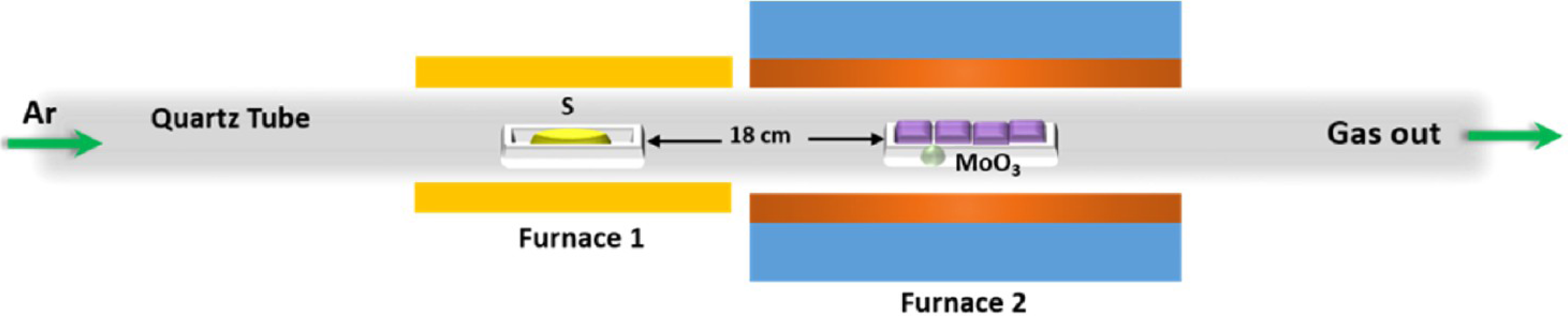
Other TMDs that compounded by CVD contain WSe
Liu et al. examined the CVD growth of WSe
Usually, the synthesis of MoS
The controlled growth of large size single-crystalline monolayer TMDs is still a challenge. Wang et al. achieved the successful epitaxial growth of two-inch single-crystal WS
Liao et al. presented controlled growth of large-area monolayer MoS
Seravalli et al. used gold nanoparticles for CVD growth of MoS
Mechanistic model for the CVD growth of 2D TMD. (a) Hexagonal MoS
Van der Zande et al. researched the monolayer direction, edge morphology, triangular domain crystallinity and grain boundary in a comprehensive study of modeling experiment, during the MoS
Ji et al. investigated the MoS
Cao et al. studied the effect of chemical potentials of Mo and S atoms on the edge structures and domain shapes of MoS
Based on the calculated energies of nucleation and propagation of various MoS
Conclusions and outlooks
In this review, the recent progress on experimental and simulation studies of the 2D materials CVD growth were summarized, including graphene, hBN and TMDs. For each material, the experimental synthesis was initially presented. Then, the theoretical studies by kMC simulations, reactive MD simulations, and DFT calculations were discussed to comprehend the growth mechanisms and the effects of reaction conditions (growth temperature, pressure, vapour-phase composition, etc.) on the domain morphologies, edge structures and grain boundaries of 2D materials. The CVD growth is a tactics which is potential to manufacture high-quality and large-scale 2D materials. Nevertheless, some knowledge-gaps still existed, especially from a theoretical perspective, this hinders the further development of understanding in the growth mechanism and engineering the controlled the 2D materials compounding.
First, the growth of single-crystal monolayer 2D material has been widely studied from a theoretical standpoint. However, the growth of polycrystalline 2D material and the formation of grain boundaries during the 2D materials merge have been rarely modelled. The modeling and simulations on CVD growth of in-plane heterostructures, such as graphene
Second, growth rate of 2D materials is still not fast and synthesis of large-scale single crystal is challenging. One possible solution is to control the domain orientation during nucleation on the growth substrate. Multiple grains with the same domain orientation are able to emerge together to form large-scale single crystal 2D material. Therefore, to predict the effect of the 2D material bottom effect precisely,more simulation and experimental work is necessary, including the effect of surface defects, steps and roughness. The competitive interactions between the layer and substrate and the edge and surface steps can also be examined.
Third, conventional experimental synthesis is time- and cost-consuming. With the development of high-throughput methodology and artificial intelligence, effective and productive experimental synthesis are desirable to establish the database of 2D materials. Using the established database, machine learning is able to further reveal the underlying mechanism of CVD growth. We believe that our review will motivate the use of high-throughput experiments, multiscale modelling and machine learning tools, and simulation to better apprehend and forecast the 2D materials CVD growth.