
Abstract
This work aims to improve the operation of multi-level inverter with reduced switching losses, thereby propose a new structure for an MLI with a reduced component count. A 27-level asymmetric Multi Level Inverter (MLI) with a minimal number of static switches is considered as a test system. The proposed MLI is developed with three input DC sources and thirteen power electronic switches. The hardware prototype is developed for 40 V and 3.5 A output. The control logic is developed in dsPIC30F410 controller. The main objective of this work is to effectively bring down the Total Harmonic Distortion (THD) of the resulting output voltage by analyzing the harmonic spectrum of the proposed MLI configuration with various low frequencies switching techniques and optimizing their switching angles and to choose an appropriate switching state using fuzzy logic controller (FLC). The proposed FLC covers wide range of operating conditions i.e. 10 switching states and variables 9*9 rules to predict the suitable switching angel. The performance metrics of the proposed structure of 27-level MLI has been evaluated upon simulation results and experimental results based on hardware prototype. The comparative study also carried out with the recent MLI topologies.
Keywords
Introduction
Recently, during the span of three decades the development of high power converters has increased in industrial applications to meet power demands and to maintain its power quality at standard level. A multi-level stepped wave based circuitry is proposed as an effective replacement in high power and medium voltage applications and also to ensure reduced distortions caused due to harmonics. Multilevel Inverters (MLIs) are power converters that produce an AC voltage from different DC voltages levels to form a staircase like waveform. Adding each DC voltage source results in the addition of a new step to the synthesized voltage output of AC power. The staircase waveform thus produced from a multilevel inverter, results in reducing the harmonics and synthesize a near sinusoidal waveform that effectively replace the conventional two level output inverter which introduces a large amount of harmonics into the supply lines. A three-phase series connected multilevel structure has employed two series connected inverter with power cells in [1]. The phase shifted multi-carrier modulation technique is employed to test the MLI. The proposed topology is differentiated from cascaded H-bridge inverter (CHB) in inverter legs connection. Both these converters comprises of the equal number of semiconductor switches on each power cell thus the output voltage levels produced in the terminals of MLI remains the same.
A relatively new configuration of a multilevel inverter with a fewer count in power switches is proposed in [2] which use series/parallel DC voltage sources which constitutes of an H-bridge with an inverter which synthesize a stepped level output by connecting the voltage sources as a combination of series and parallel voltages. This topology of inverter can generate increased voltage levels by extending the same using the same methodology. This configuration of inverter is controlled by a hybrid modulation method. A 15-level inverter is proposed which requires 14 switching components and 3 dc voltage sources. Hybrid modulation technique is used for the MLI control has produced voltage THD of 6.80%.
In [3], a new structure of a multilevel converter circuitry utilizing minimal number of power semiconductor switching components is proposed and analyzed the magnitudes of the different dc source voltages. The intended topology is designed to reduce the switches count, its associated gate drivers, clamping diodes and blocking capacitors but still manage to produce maximum output levels. It can be found that the first recommended topology can produce 125 levels output utilizing only 24 IGBTs and the second topology can produce161 levels output indulging 28 IGBTs. The asymmetrical configuration with trinary voltage sources delivers the higher voltage levels with the available quantity of IGBTs. A multi-level inverter topology built on switched dc sources comprising of a lower count of components, adopted for higher output levels is discussed [4]. It includes fluctuating input dc sources connected alternately with one another through power electronic switches. Each input dc comes in to the load independently or combined with other input levels for high voltage step-up. Similarly, [5] discussed about a new configuration of a series connected H-bridge multilevel converters with reduced circuitry for applications that demands high voltage magnitude. The topology proposed is based on connecting single-phase sub-multilevel converter in series with full-bridge converters. When comparing with the other conventional types of multilevel bridges, the count of dc sources, power switches, and the cost of power converter is considerably less when the output voltage level increases. Three methods are projected for deriving the voltage magnitudes of the input dc voltage sources required for the circuitry.
A generalized topology of a cascaded multi-level inverter structure using series connected of sub-multilevel inverters is discussed in [6–9]. A new structure constituting sub-multilevel inverter is thus proposed employing minimal number of switching devices which can be operated equally in modes of symmetric and asymmetric voltage source relation. Obtaining optimal configurations regarding diverse criteria such as the count of switches and dc voltage sources are taken as the key issue.
A cascaded half-bridge along with a multileveled dc link utilizing a fixed dc source voltage is connected accordingly to provide outputs of the required voltage levels in [10–12]. The staircase modulation scheme employing fundamental frequency is adopted to simulate the corresponding switching gate signals and extended for n-levels. A novel hybrid cascade-stack (HCS) converter with a reduced switch count has formulated in [13]. The basic unit employed essentially comprises of two numbers of dc sources with constant magnitude and four main power semiconductor switches which are assisted with an auxiliary unit that employs two IGBTs and a dc voltage source. The circuitry is discussed for both symmetric and asymmetric configurations and the same is verified by simulating the outputs for 11-levels, 23-level symmetric types and 31-level asymmetric mode. In [14, 15], a fuzzy logic controller is more appropriate for lower order harmonics rejection and also to get the expected fundamental output voltage. Various dynamics affect the choice of values for dc voltage sources that are used in MLI. The time varying dc sources as in case of renewable energy sources or battery sources with different charging states are taken as 11- level MLI fed sources whose switching angles has to be modified in tune with the Artificial neural networks (ANN) as explained in [16] which is then applied to generate switching angles analogous to instantaneous values of the varying dc sources.
Problem statement
It is simpler to synthesize a high power level and a high level voltage inverter adopting the MLI topology, where the voltage stress of the semiconductor switches can be efficiently regulated. The voltage level increment in the inverter does not require upgrading the individual devices to a higher rating of the system as mentioned in [17–20]. The exclusive structure of multilevel inverter allows the system to achieve high voltage levels with very low distortions without the use of transformer, by series connection of supply DC sources using appropriate switching devices. The MLI consumes input current with a lower distortion and could be effectively worked in the fundamental frequency ranges of switching and also can be extended to high switching frequency Pulse Width Modulation (PWM) in [21, 22]. Thus, MLI has become an effective replacement as a solution to be operated with medium and high voltage levels with reduced harmonics.
The power quality of the generated output can be substantially improved by increasing the number of output voltage levels. When the number of voltage levels in the output is raised, it results in the harmonic distortion found in the output voltage waveform to decrease significantly but it leads to the usage of large number of power switches and its gate drivers, increasing the complexity, the switching losses thus produced by the switches results in reduced efficiency and reliability
Contribution and problems solution
The main objective of this work is to reduce the complexity involved in the practical realization, reducing the number of switches even with higher levels, without perturbing the power quality. Therefore a novel MLI configuration is investigated to generate 27-voltage levels utilizing a three input DC sources and thirteen power electronic switches. The major contribution is prediction of optimal switching angles between different voltage levels to eliminate the value of output voltage THD. The fuzzy logic controller (FLC)is used to identify the exact positions of switching angles to activate the MLI switches as mentioned in [23–28]. There are 10 sets of fuzzy switching sequences with 9*9 rule base for the prediction of optimum switching angles are developed and presented in this work.
This overview of the paper is organized as follows. The modelling of a novel asymmetric MLI and its various switching level are presented in Section 2. The optimal selection of switching angles using FLC is discussed under Section 3. Results obtained from Simulation and hardware prototype are highlighted under Section 4. Conclusions about the findings are included under Section 5.
Modelling and operation of 27-level asymmetric multi level inverters
In multi-level inverter, the output voltage level reduces when DC source voltages of equal magnitude termed as the symmetric configuration. An asymmetric configuration with unequal voltage sources magnitudes are selected to increase the number in the voltage levels in the output.
The proposed circuitry is synthesized with three input dc sources

Proposed 27-level asymmetric MLI topology.
The necessary dc voltage sources for the proposed MLI configuration can be given by
For an asymmetrical MLI, the magnitude of input DC voltage has a trinary relationship that is expressed as
Where i = 1, 2, 3 ... n, and the magnitude of the dc sources varies by the ratio V
s
, 3V
s
, 9V
s
etc.The number of levels in the output voltage that can be synthesized out of an asymmetrical binary configuration is presented as
The maximum value of the generated output voltage is estimated from Equation (5)
In the proposed MLI, three voltage sources has been considered, they are V s1 = 3 V, V s2 = 9 V and V s3 = 27 V respectively. The total number of power electronic switches required is estimated as 13 from Equation (2). The switches are connected in series with the voltage sources such as S 1, S 2, S 3 and S 4 cannot be turned ON directly, the complementary switchesS 5, S 6, S 7, S 8 and S 9 are connected in parallel to the voltage source so as to avert a possible short circuit.
The switching states of the power switches are utilized to synthesize an output V o . These different switching patterns and all the possible output levels of voltage of an asymmetrical configuration supplied with three voltage sources are presented in Table 1. The switching arrangement are presented for the aforesaid multilevel inverter structure, which will be able to generate a zero state and 13 positive and negative states, producing a 27- level output voltage. The operation in detail of the proposed configuration is examined for its different switching states and different states of the output voltage are presented in the Fig. 2 and Fig. 4. This details the different switching states and their various modes and of operation as stated by Table 1.
Switching states of an asymmetrical trinary configuration
Switching states of an asymmetrical trinary configuration

Various switching states for positive output voltages(a) Vs3, (b) Vs2 –Vs3, (c) Vs2, (d) Vs2 +Vs3, (e) Vs1- Vs2 - Vs3, (f) Vs1- Vs2, (g) Vs1- Vs2+ Vs3, (h) Vs1- Vs3, (i) Vs1, (j) Vs1+ Vs3, (k) Vs1+ Vs2- Vs3, (l) Vs1+ Vs2.
In Fig. 2, the twelve switching states of MLI for positive voltage magnitudes are presented. The switching sequence for 0, + (Vs1+ Vs2+ Vs3) are presented in Table 1. Similarly, Fig. 6 illustrates remaining twelve switching states for negative voltage and -(Vs1+ Vs2+ Vs3) is presented in Table 1 Many researchers have proposed a H-bridge at the output to generate positive and negative sides of the MLI. In this work, the four switches of traditional H-bridge circuit is replaced by three switches namely S11, S12 and S13.on the basis of these voltage levels which are identical and appropriate modulation control of the switching angles, a voltage output waveform similar to a staircase can be generated.
The switching losses reduction in an MLI has to be ensured to realize a more flexible and efficient structure and with structures operating upon lower switching frequencies, low-order frequency harmonics could be observed. Many approaches has been adopted for excluding these low-order frequency harmonics but the most conventional method in widely preferred in MLI for achieving a better THD is the SHEPWM technique which generally adopts solving nonlinear transcendental equations which characterizes its harmonic content for determining the switching angles. The circuitry can be simulated for asymmetrical configuration and the various switching pulses for the circuit from S1 to S13 are generated with suitable angles. The switching angles are optimized using FLC controller. The results obtained through simulation are presented in Section 4.
A 27-level inverter structure as proposed in section 2 is employed for implementation of voltage sources as per Table 1 with voltages ranging from 0, V s , 2V s , 3V s ... 13V s could be employed for different output voltage levels. Figure 3 shows the different switching angles to be calculated for adopting the switching states for quarter cycle of operation or a sinusoid. For operation between 90°, switching angles varying from α1 to α13 are to be calculated which are to be determined to lower the harmonic content in the voltage output resulting in the reduction of the THD and improve the power quality.
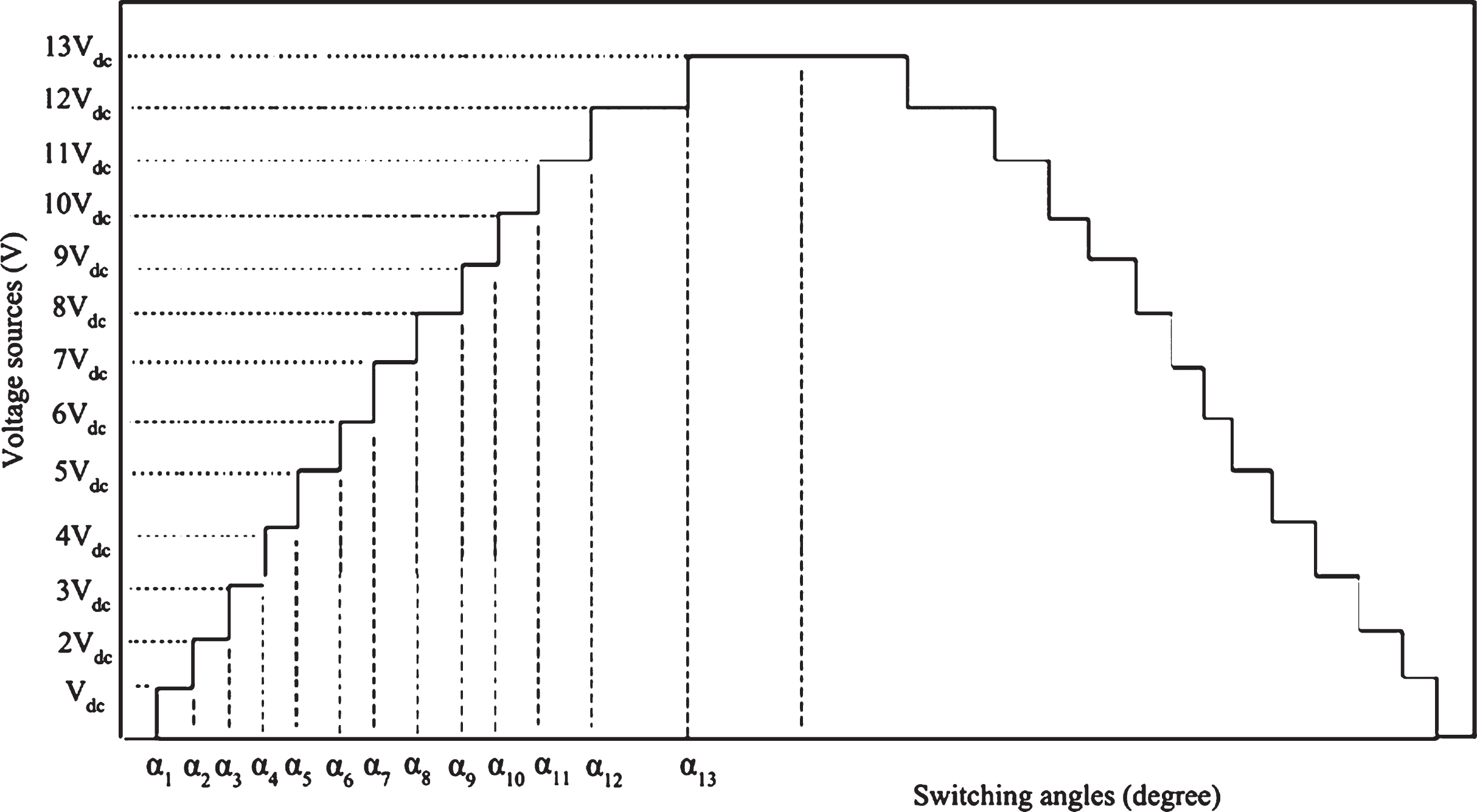
Output voltage waveform at various switching angles.
The fundamental equation for sine waveform is given in Equation (6). Initial generations of switching angles are obtained from the reference signal phase angle θ
i
. The Coordinate Rotation Digital Computer (CORDIC) approximation method which is otherwise known as the Volder’s algorithm is used to generate reference switching angle for fitness value (f
v
) generation and comparison.
The CORDIC approximation method uses Direct Lookup (DLU) and Linear Interpolation (LI) strategies for computing the results. Compared to the DLU, the LI methods have the higher accuracy and reduce the error in the approximation.
Where, N varies between 0 to 255 and “s” denotes the number of switching angles which is 13. Reference/ targeting switching angles are obtained from the following CORDIC approximation Equation (7). The main objective of switching angle prediction is primarily to eliminate harmonics by reducing the content of output voltage THD.
Compared with the selective harmonics elimination (SHE) PWM proposed CORDIC approximated signal with MLT adjusts the switching angle based in THD level from the following equations
Compute f
v
as per Equation (8), when the THD content of an MLI output voltage is not more than 5% and single harmonic content from the fundamental voltage is not more than 3%. The switching angles are generated randomly to satisfy the following constrain as per the Equation (9).
Where, θs → θ1 < θ2 < θ3 … . < θ13 < 900 and θ s is the switching angles and M is the modulation index that varies from 0 to 1.
The normalized switching angle of the aforesaid MLI is presented in Table 2. The quantity of THD content in the output is sensibly reduced by adjusting the modulation index (M).
Reference switching angle from CORDIAC method
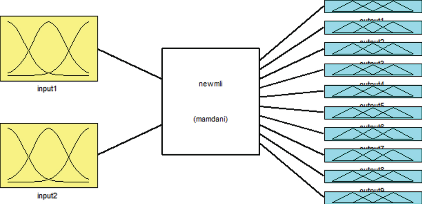
The fuzzy logic controller is implemented for obtaining switching angles for the 27 level MLI, operated in the trinary asymmetric mode with 3 voltage sources of magnitudes Vs1 = 216 V, Vs2 = 72 V and Vs2 = 24 V giving a peak magnitude of 312 V. The FLC has two inputs, one is modulation index and the other is the error taken between the switching angles of a sine wave which is taken as the reference wave based on which the switching angles are generated and the current output voltage. There are ten outputs. The FLC employs a triangular membership functions both for input and output membership function. The Membership function plots of the inputs and the outputs as shown in Fig. 5.
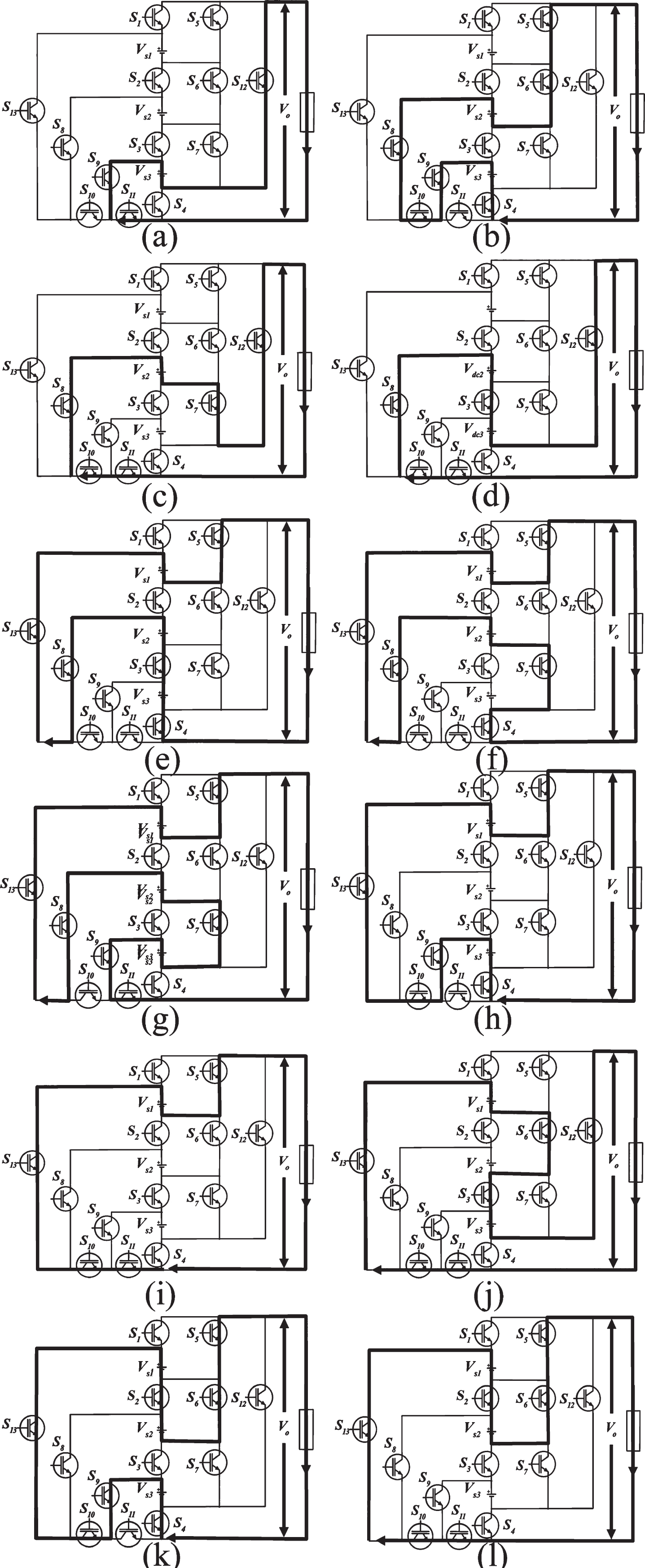
Different possible switching states for negative output voltages (a) -Vs3, (b) -(Vs2 –Vs3), (c) -Vs2, (d) –(Vs2 +Vs3), (e) –(Vs1- Vs2 - Vs3), (f) –(Vs1- Vs2), (g) –(Vs1- Vs2+ Vs3), (h) –(Vs1- Vs3), (i) -Vs1, (j) –(Vs1+ Vs3), (k) –(Vs1+ Vs2- Vs3), (l)-(Vs1+ Vs2).
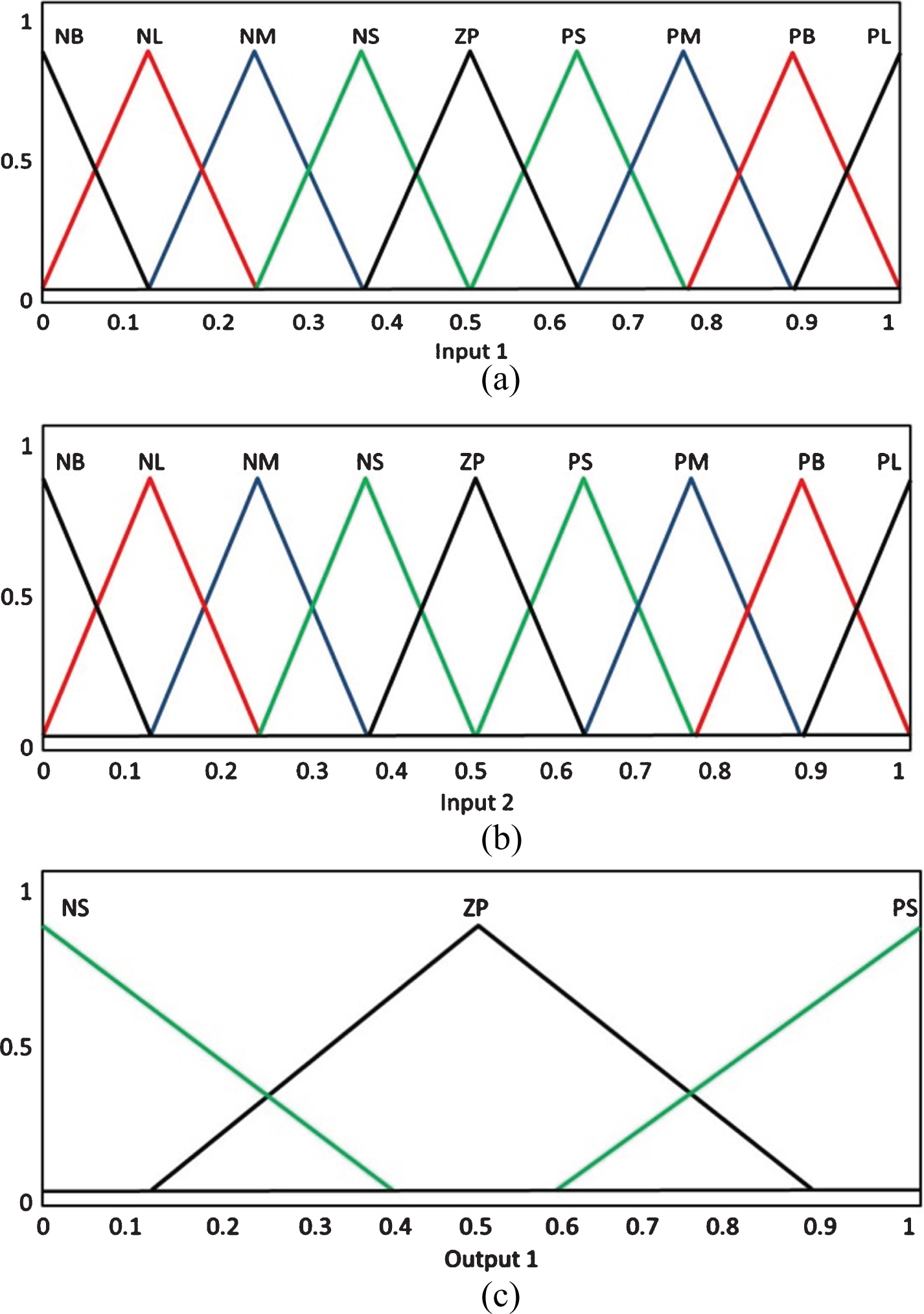
Membership function plot of (a) Input 1 and (b) Input 2 and (c) the Outputs from1 to 10.
The inputs fuzzy partition have nine terms varying from NL to PL. (NL, negative large; NB, negative big; NM, negative medium; NS, negative small; ZP, zero point; PS, positive small; PM, positive medium; PB, positive big; PL, positive large); The output has only three membership functions NS, ZP and PS. Based upon the input values the output changes from the three state NS, ZP and PS in the fuzzy partition. When the output is greater than ZP or ≤ PS then the corresponding switch of the MLI is turned ON or else the switch is turned OFF. With the help of the two input membership functions ten outputs membership functions are taken for controlling 10 switches of the MLI.
The Fuzzy Inference System Editor is as shown in Fig. 7. which shows the inputs and the outputs of the FIS as governed by the rule base.
Fuzzy inference system editor.
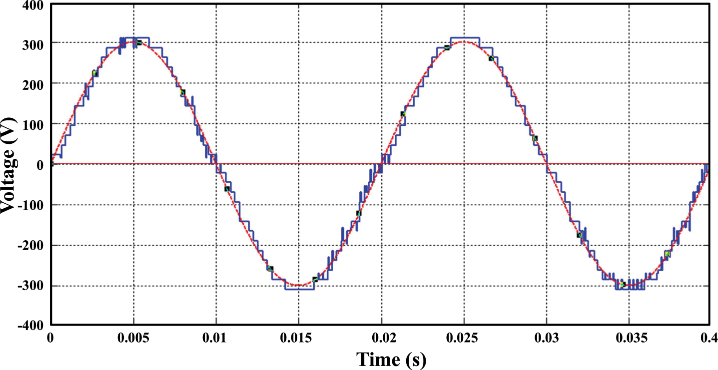
Output voltage of FLC with carrier frequency of 500 Hz and modulation index = 1.
The fuzzy rules are formed using Mamdani rules set and a Matlab fuzzy logic tool box is used for the fuzzy logic control. This tool box aids the input and output variables for the formulation of rules for the fuzzy controller. Accordingly, a 9*9 rule base is derived for the ten output states and is tabulated as a lookup table. The modulation index is varied manually with the input reference sine wave and the THD of the simulated output voltage is observed using the MATLAB simulation model. By doing so the switching angles of these operating switching states gets varied to generate the output with reduced harmonics by performing the above operation based on the lookup table to obtain the desired crisp set of the output. The rule base relating the input membership functions with the outputs while each output represents the state of the 10 corresponding switches can be tabulated and can be represented as tables shown in Table 3. The switching states cannot be expanded beyond these limits. If it is expanded then the MLI has severe short circuit between the switches that leads to switch/circuit failure or caused poor output voltage and THD.
Fuzzy rule base for an asymmetrical trinary configuration

The projected structure can be realized for all these three relationship of symmetrical and both asymmetrical modes pertaining to the dc sources magnitude. It is observed that asymmetric mode of source produces the highest number of voltage levels of the output operating in the trinary relationship of dc voltages and the THD obtained is lesser compared to the other symmetric and asymmetric modes. It can also be noted that, as the number of dc sources increases, adding a few power switches can produce outputs of larger levels. Increasing the number of output levels for increased dc voltage sources requires a complex control but the resulting power quality of the output can be sufficiently enhanced.
Simulation results
The proposed structure of circuitry is synthesized with simulation tools of MATLAB/ Simulink with its timing sequences.
The modulation index is varied manually with the input reference sine wave and the THD of the simulated voltage output is obtained from the MATLAB simulation model. By doing so the switching angles of these operating switching states gets varied to generate the output with reduced harmonics by performing the above operation on the basis of the lookup table to obtain the desired crisp set of the output.
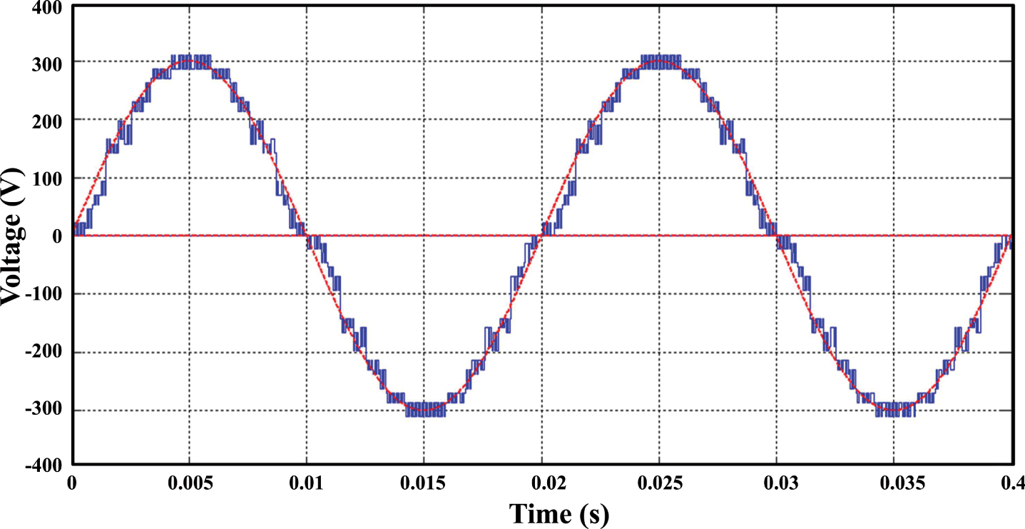
The FFT spectrum of the output voltage with carrier frequency of 1000 Hz and 500 Hz are analyzed with modulation index 1. Overall 20 cycles are observed for THD and corresponding voltage magnitudes and THD spectrum are presented in Fig. 7 to Fig. 10. It is found that the THD obtained for the synthesized output voltage waveform is 5.93% for the first 10 cycles, 5.89% for the next 10 cycles and 5.89% for the overall 20 cycles. The results are taken for this carrier frequency for various modulation indices like 0.7, 0.75, 0.8, 0.85 and 0.9.
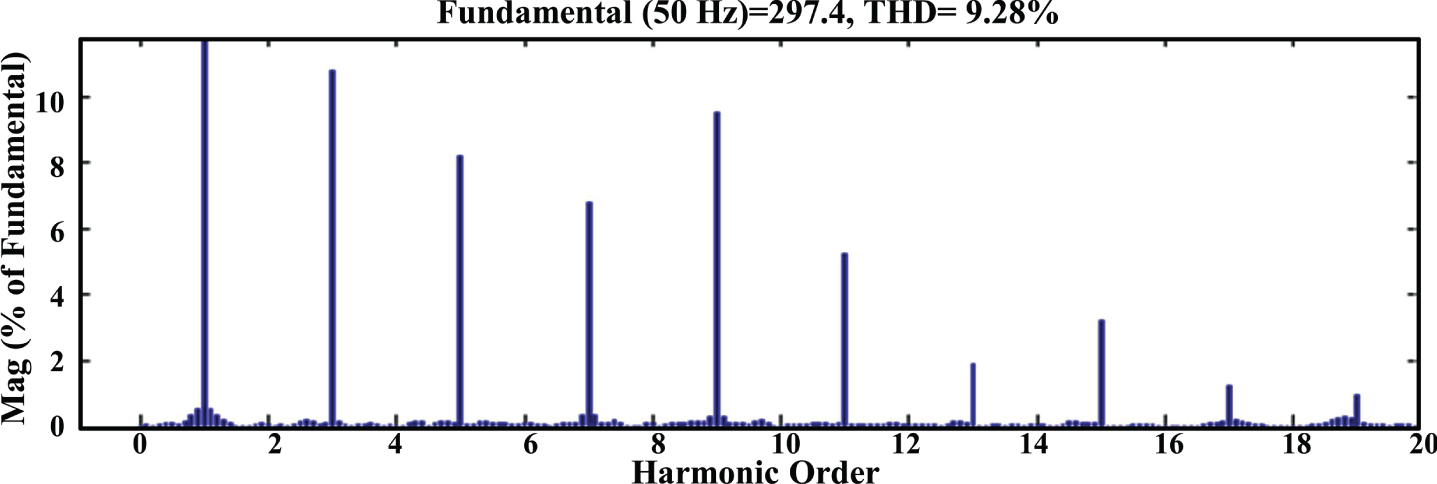
FFT spectrum of FLC output with carrier frequency of 500 Hz and modulation index = 1 for the overall 20 cycles.
Output voltage of FLC with carrier frequency of 1000 Hz and modulation index = 1.
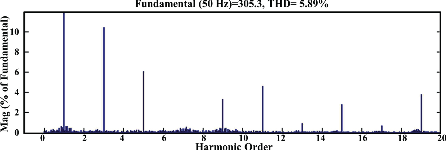
FFT spectrum of FLC output with carrier frequency of 500 Hz and modulation index = 1 for the overall 20 cycles.
To validate the correctness and to verify the projected topology, a hardware prototype for 27 output level multilevel inverter is developed. The hardware setup of the proposed MLI structure that constitutes of 10 power IGBT (GN2470) switches which has a voltage and current rating of 40 V and 3.5A respectively is shown under Fig. 11. The proposed hardware structure utilizes an asymmetrical mode of voltage sources with a trinary relationship having three dc voltage sources.
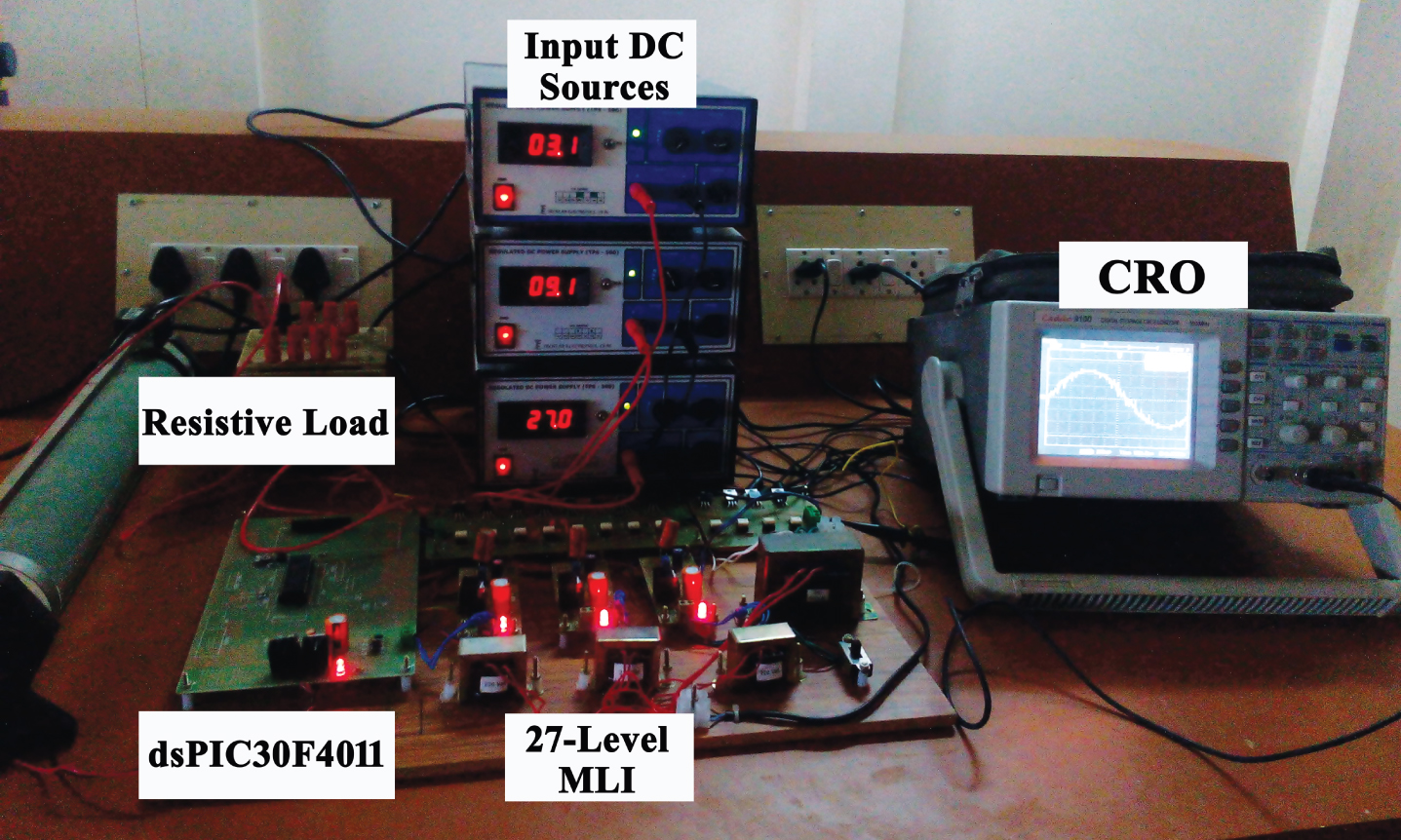
Experimental setup of proposed 27-level MLI.
In the hardware prototype employing a trinary asymmetrical mode of voltage source relation, three voltage sources with magnitudes of 3 V, 9 V and 27 V are taken as voltage inputs. The dsPIC30F4011 controller is used for gate switching pulses generation. The pulses for the various switches ranging from S1 to S13 are shown in figures from Fig. 12(a) to Fig. 12(f) for synthesizing a 27 level output voltage waveform.

PWM pulses of a 27-Level MLI switches(a) S9 (b) S1, S5 (c) S8, S11, (d) S2, S6, S12 (e) S4, S10, (f) S3, S7, S13 .
The output voltage waveform obtained after the implementation of the gate pulses shown in Fig. 13. This is obtained when an asymmetrical trinary input dc voltage relationship is employed with three dc sourced used yields a 27 level voltage output.
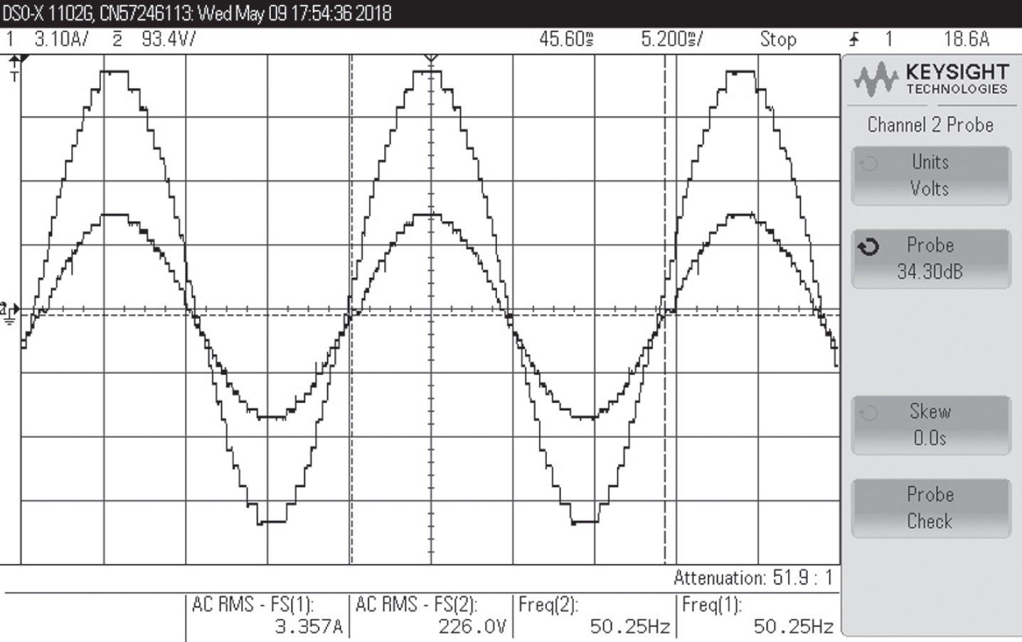
Output voltage and current of 27-Level MLI.
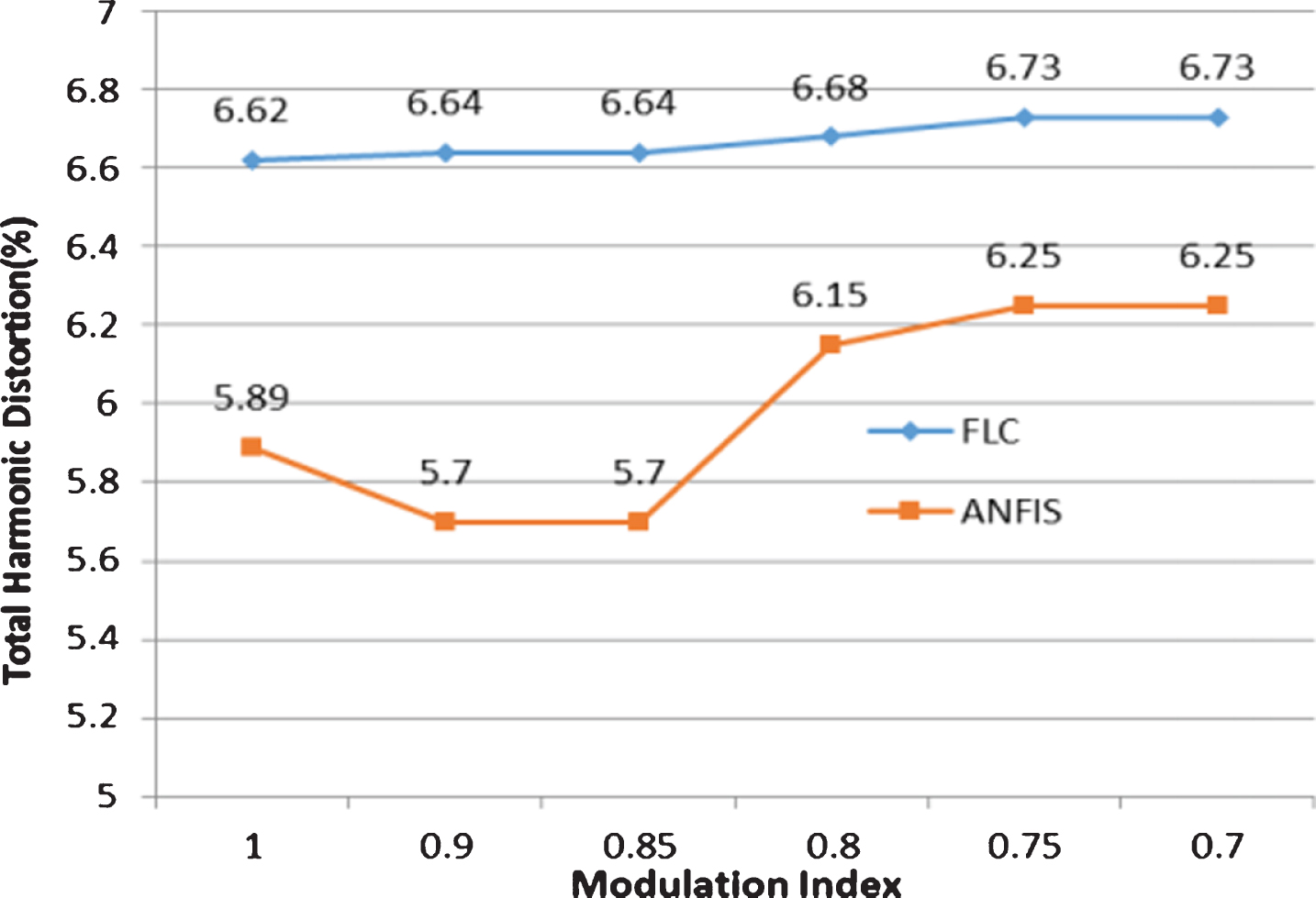
It can be found from Fig. 14 and Fig. 15, the comparison of the THD obtained for different modulation indices, at 500 Hz and 1000 Hz respectively by the FLC and ANFIS controller. FLC controller has obtained better power quality confirming that it has yielded optimized switching angles that has resulted in bringing down the harmonic content in the output voltage.

Modulation index (M) vs FLC and ANFIS at 500 Hz.
Modulation index (M) vs FLC and ANFIS at 1000 Hz.
The proposed multilevel inverter structure can be extended to any output level of voltages with positive and negative levels at the output terminal. In the proposed work, a new 27-Level MLI without H-bridge is introduced and it uses 13 switches to generate positive and negative cycles of output voltage. The projected converter is analysed by MATLAB Simulink and validated using hardware prototype. The ten switching states developed in FLC for switching angles prediction of the converter reduced the THD content with in 5%. The hardware setup is developed for 40 V, 3.5 A output using dsPIC30F4011 controller. The simulation results along with the experimental results are clearly presented. In future work, the number of switches used in the proposed MLI topology can be less than 13. This may provide a chance for increasing more switching states in FLC which results in higher voltage levels in the output. The improved MLI can be used for the shunt active filtering application to maintain the power quality of single-phase distribution line. It can also be used as a dynamic voltage restorer or variable AC voltage regulator for single phase induction motor drive application. Based on the results, it is observed that the proposed structure of MLI will provide a better performance for getting higher voltages with less number of power switches in the circuitry.