
Abstract
In this paper, the design and simulation results of a general-purpose fuzzy logic controller (FLC) with mixed-signal (analog and digital) inputs and digital outputs are presented. Based on a new strategy, it provides simplicity and high speed from the analog prospective and a total digital system advantages with unchanged digital system properties. A novel and reliable structure with respect to other topologies for the fuzzifier section is designed which enhances the accuracy and the velocity. In order to detect minimum and maximum of the input currents at the same time, an inference engine consisting of a min & max circuit is an addition. The benchmark for the defuzzifier in the proposed design is simplicity and through a simple approach, the center of area (COA) is attributed to the defuzzifier. The proposed controller circuit consists of two inputs, sixteen rules and one output designed in 0.35μm CMOS standard technology and simulated with MATLAB systematically. The total controller circuit is simulated with HSPICE simulator (BSIM3v3 parameters) and the layouts were extracted with Cadence Virtuoso v 5.1. The inference speed of the controller is about 41.3 MFLIPS (fuzzy logic inference per second) and power consumption is 3.2 mW.
Introduction
Nowadays, fuzzy logic is extensively used in designing systems. This logic has a great deal of flexibility and it is close to human mind so it makes the process of controlling systems easy. The applications of fuzzy controllers have been significantly grown in many areas such as wind turbine, traffic light controller [1] robotics, mobile devices, advanced human-machine interfaces, smart sensors, home applications and antilock-braking system (ABS) of vehicles and smart machines that can analyze and diagnose issues without the need for human intervention [2].
The major advantage of fuzzy logic controller is that it admits imprecision of data, thus, is able to model reality better than the traditional digital logic. In other words, traditional digital logic only describes black and white, while fuzzy logic describes interval between black and white as well. In real life, situations are often described by linguistic terms. Fuzzy logic controller can represent and process data and generate results in these linguistic terms as well. Hence, fuzzy logic rules are more powerful in data processing. However, due to demand for higher speed and more compact hardware, analog VLSI is becoming more and more important in the design of fuzzy logic controller technologies [3].
There are two general approaches for using fuzzy logic in control systems, software, and hardware. Software-based fuzzy controllers are limited to a slow-speed operation and so they are not efficient for real-time applications. In comparison with software, hardware approach is faster, which can be made as discrete or integrated circuits. Fuzzy chips are the most ideal form of hardware solutions for fuzzy controllers.
In fuzzy controllers three realizations of analog, digital and mixed analog and digital are possible. A digital or analog fuzzy controller is well defined through its connections and internal structure. Digital fuzzy controllers can connect to digital sensors and their remarkable benchmark is their ability in processing digital signals. Providing a reliable connection to other counterparts, besides the ability of saving and keeping data in digital systems makes them robust over noise and distortion. Analog fuzzy controllers on the other hand are able to process analog signals and the output voltage or current which is produced in sensors or other electronic devices is becoming the input data for these controllers. For any of these structures there have been lots of applications including [3– 5, 18] which are analog samplers and [6, 7] which are topologies in VLSI. Mixed analog-digital fuzzy controllers include digital interfaces which have analog circuitry inside their structures [8, 9]. In order to have a reliable structure with the optimum performance, we proposed a new CMOS integrated circuit to implement fuzzy controller chip with mixed-signal input and digital output, while the internal blocks (Fuzzifier, Inference and Defuzzifier) are realized by current mode analog circuits. The proposed controller circuit consists of 16 rules which illustrate the relation between controller’s inputs and outputs. Controllers can be used for different purposes by changing the value of the rules. The digital output of this controller can be easily used wirelessly with other circuits, sensors and machines for industry 0.4 that is already seeing factories become increasingly automated and self-monitoring as the machines within are given the ability to analyze and communicate with each other [2]. The proposed fuzzy controller with its new Fuzzifier can obtain four different types of S, Z, Trapezoidal and Triangular membership function shapes and it is possible to program it to change suitable slope of shapes. The reminder of the article is as follows: section 2 is attributed to explaining the main idea of the fuzzy controller, new and improved Fuzzifier, Min– Max operators, Multiplier/Divider, current mode A/D converter. System simulation, circuit layout and control surfaces which provided by Hspice simulations and Matlab software are presented in section 3. Finally, the conclusion and comparison part is in section 4.
Proposed fuzzy controller
Main block diagram of system
Figure 1 shows the complete block diagram of proposed FLC with 2-inputs (each input has 4 language terms) and one output with 7 singletons (VVS, VS, S, M, L, VL and VVL) using COA for defuzzifying, Min & Max circuit for combining antecedents of each rule, and product– sum inference method for performing system deduction.
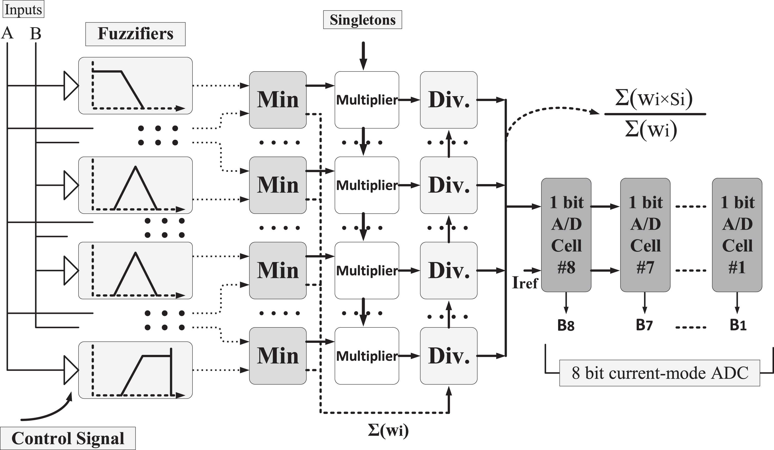
Main blocks of proposed controller.
In this article, a novel fuzzifier is illustrated in which the output and the input are in current mode. The circuit includes digital and analog parts that mean we have a mixed mode fuzzifier. This fuzzifier is capable of producing S, Z, triangular, and trapezoidal shapes and it is programmable for slope and height altering and horizontal shifting through 7 switches. The advantages of this membership function generator (MFG) are high speed, low power dissipation, and low error.
The proposed circuit is depicted in Fig. 2 and as you can see, the input current equals Iin-Ix in which Ix is exploited to shift MFG’s output horizontally. Transistors Mx1 and Mx2 act like a diode and accompanying with PMOS current mirror, they have the responsibility to rectify Iin-Ix. According to Fig. 2a, if the value of Iin-Ix is positive then transistor Mx2 remains in cutoff region and transistor Mx1 turns on and consequently the value of output current equals Iin-Ix. On the other hand, if the value of Iin-Ix is negative then transistor Mx1 remains in cutoff region and transistor Mx2 turns on. This time the current pass through a PMOS current mirror and the output current equals -(Iin-Ix). In addition, the current of transistors Mx1 and Mx2 are controlled by switches S0 and S1 and with the proper condition of these two switches, Z-shape and S-shape outputs will be available.

The proposed fuzzifier.
The digital programmable current mirror (PCM) block is shown in Fig. 2b in which the input current is the output current of rectifier. Table 1 is attributed to the size of the transistors.
Transistor proportional size
Current IS is subtracted from input current of programmable current mirror block and it determines the upper width of the trapezoid (if IS = 0 then the output will be triangle). For better understanding, the output current of PCM is reflected on equation (1).
It is worth noting that Iref is added to the circuit in order to control the height and the reference point of output shape (trapezoid or triangle). Hence the total output of the circuit can be shown in this equation.
The used min– max circuit is depicted in Fig. 3. Operation of the circuit is based on the modified-Wilson current mirror in bottom of the Fig. 3 which produces equal current in the branches under nodes A and B. If we assume one of the input currents (I2) increases and (I1 < I2), this rise causes a voltage increase at the node B in comparison with the node A. As a result of this difference, M13 will turn on and M14 will turn off, hence an extra current equal to I2-I1 is conveyed to the other current mirror through M13 and it will be added to the minimum current of inputs (I1) to produce the maximum output of the inputs which in this case is I2. In other words, to obtain maximum of the inputs, the absolute difference between two inputs (|I1- I2|) is added to the minimum current value of them. Similarly, if (I1 > I2), then node voltage of A increases in comparison with the node voltage of B. So, M13 will be off and M14 will be on and the extra current (I1- I2) is transferred to the current mirror through M14 and will be added to the minimum current of the inputs to produces the maximum value of the two input currents. Considering that the input currents are equal, two node voltages of A and B will be equal and both transistors M13 and M14 will turn off. In this case, both output currents of the circuit, minimum and maximum, are equal. Using this structure, both minimum and maximum of the inputs are simultaneously detected.
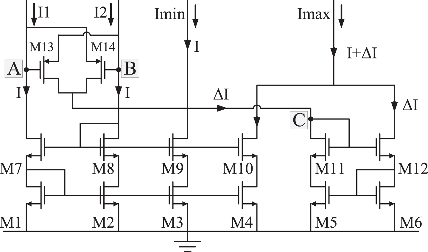
Min & max circuit.
The outputs coming from inference engine section is fuzzy data which describes the performance of the controller in fuzzy mode. For scientific applications, processing crisp data is easier than processing fuzzy data. So an interface, named as defuzzifier is needed for converting fuzzy data into crisp data. Here the center of area (COA) is exploited because of its flexibility and low error. The COA equation can be seen in equation 1 as follows:
K is the number of independent fuzzy elements and μc (zi) is the weights of rules (currents) which is produced in inference engine. In order to implement a circuit based on equation 1, a multiplier/divider circuit is needed to perform the currents multiplication and division actions. It is not required to use adder circuits since this is a current mode defuzzifier and the adding process is accessible through connecting wires.
Before talking about the main circuit, the structure in Fig. 4 is described. It acts simultaneously as a squarer and divider. If there is a current with the value of Iin coming out of node X, then we will have:
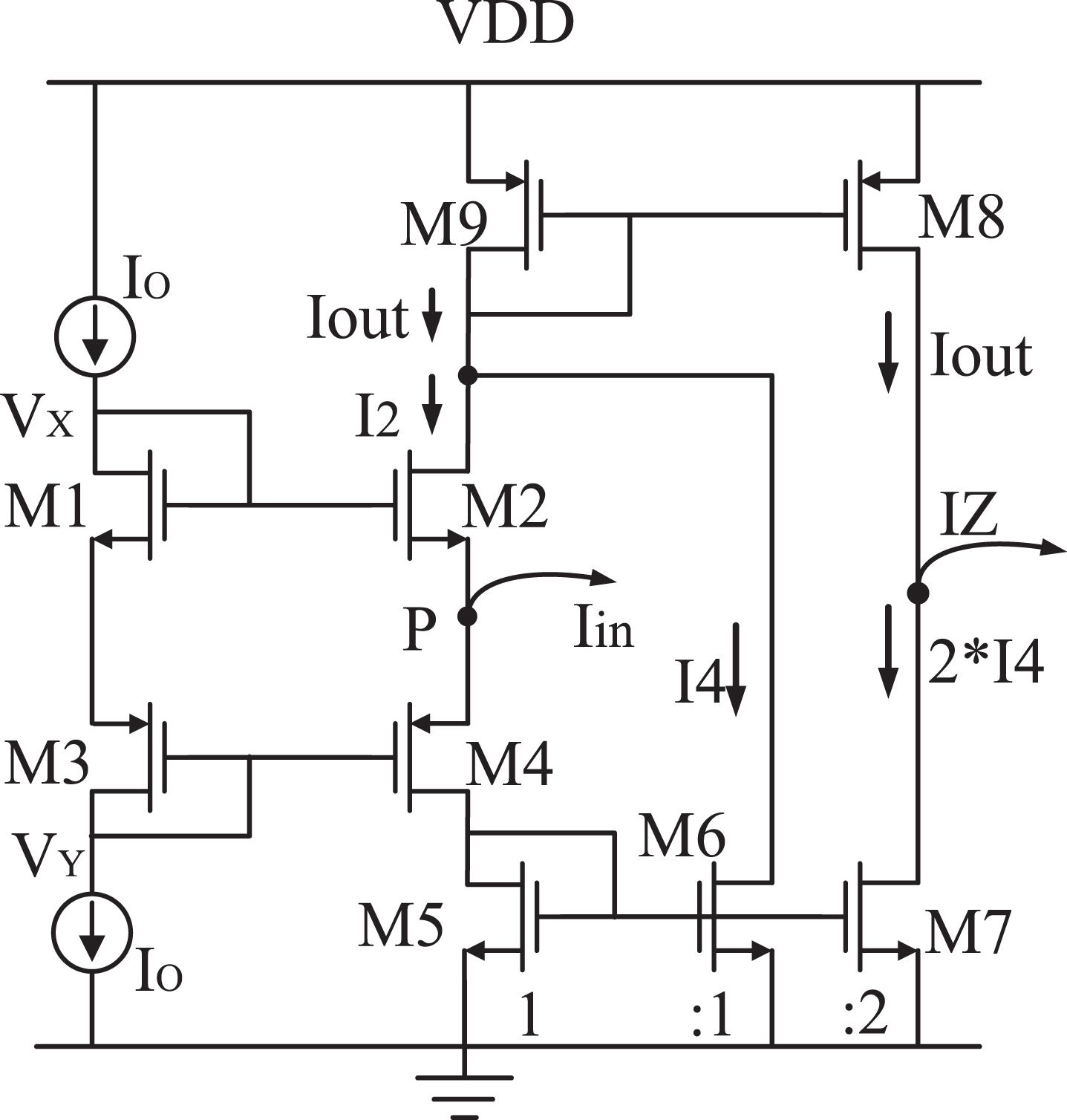
Squarer circuit.
In order to implement the multiplier/divider circuit, two squarer circuits are used which can be seen in Fig. 5. If the addition and subtraction of two currents Imin and Isi comes out of nodes X and Y, respectively, we will have:
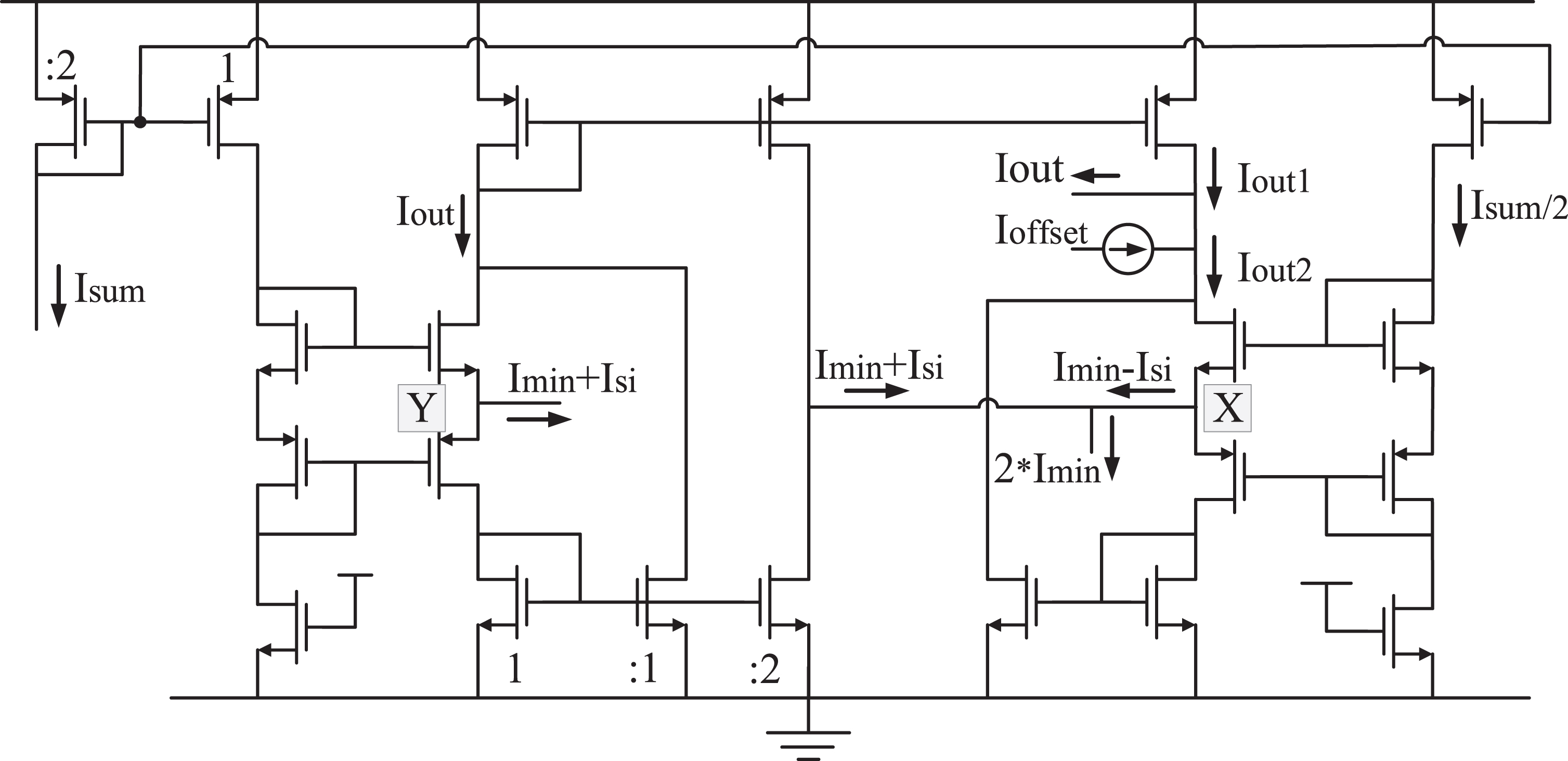
Multiplier/divider circuit.
The subtraction of these two values in node OUT will be as follows (with a little offset):
In equation (7), Imin is the result of min & max circuit from inference engine section, ISi is the singleton current related to the weight rules, and Isum is the total of weight rules or in other words it is the total of all min & max circuit’s currents. Hence, the COA approach which is reflected in equation (3) is achieved.
Considering the advantages of having digital outputs for controllers, we proposed an improved circuit based on successive approximation technique that provides a current mode A/D converter with 8bit resolution accuracy. According to the Fig. 6, two currents of I (obtained by multiplying two currents of Imin and Isi and divided by the current Isum in Fig. 5) and Iref are applied to the MSB cell. This structure employs continuous time algorithm data converter whose input currents of IIn and IREF are compared to each other and digital outputs are defined. The current of Iref is mirrored in all cells and having condition of (IIn < Iref), transistors M1 and M2 double the current of Iin to provide mentioned condition. At node A, 2Iin and Iref or in other words Iin and Iref/2 are compared.
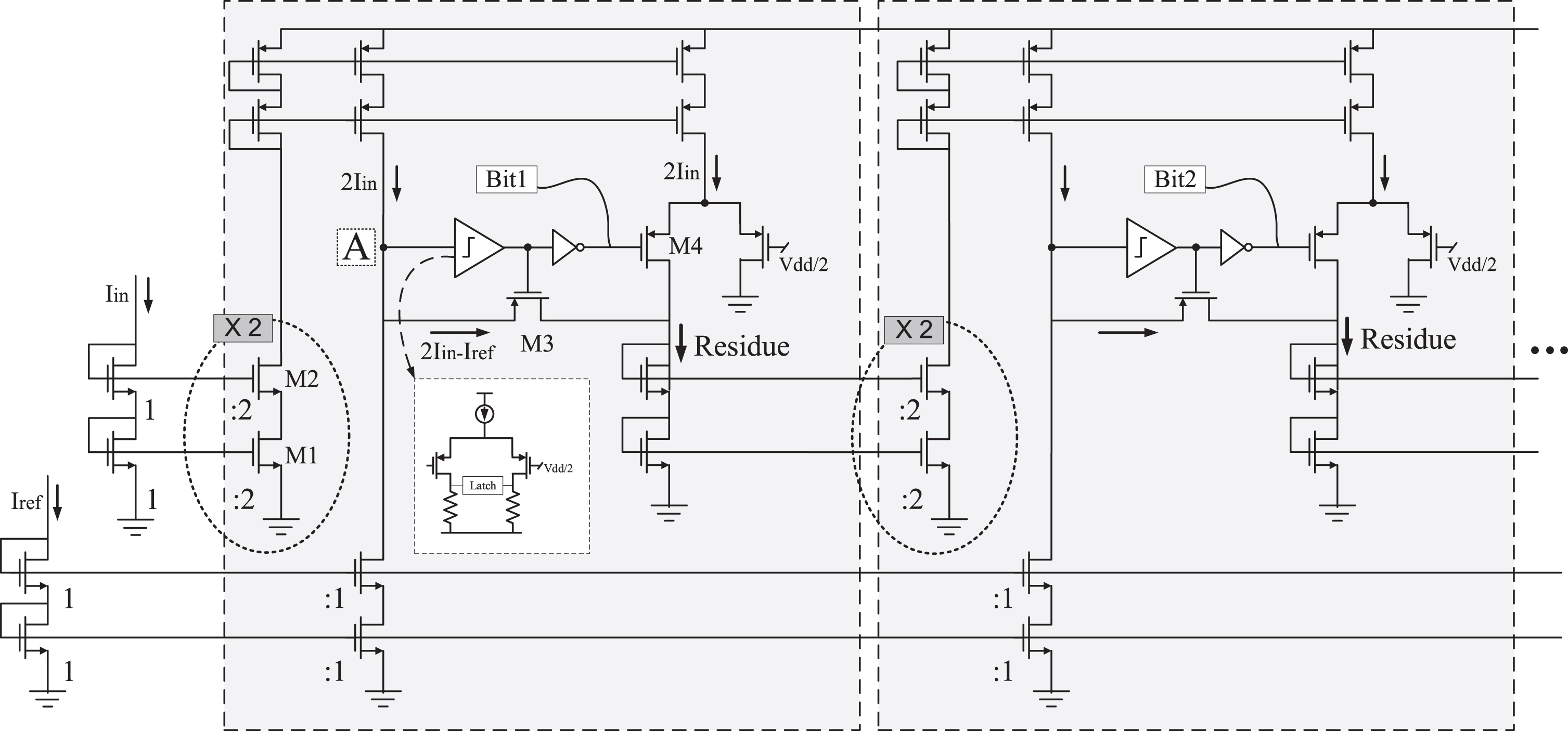
The bit cell circuit of current mode A/D converter with applying currents of Iin and Iref in two most significant bits.
(1) If Iin > Iref/2, the voltage of nod A will be high and using simple current comparator, the output of nod Biti results logic “1”(Biti = “1”); in this state, the residue of (2Iin – Iref) enters next stage input via M3.
(2) If Iin < Iref/2, the voltage of nod A goes low and then logic “0” will be obtained in output of nod Biti (Biti = “0”) and residue = 2Iin. Therefore the transistor M4 is conducting and the current of 2IIn enters the next cell.
The proposed employed continuous time algorithm data converter bit cells are better than other previously reported works [10, 11], because the residue is multiplied by gain 2 in each stage, then the comparator performs the comparison task more accurately. In this design, to achieve 8-bit accuracy, it only needs to have a mirror miss match of less than 1/64, which is easily achieved by common centroid lay out method.
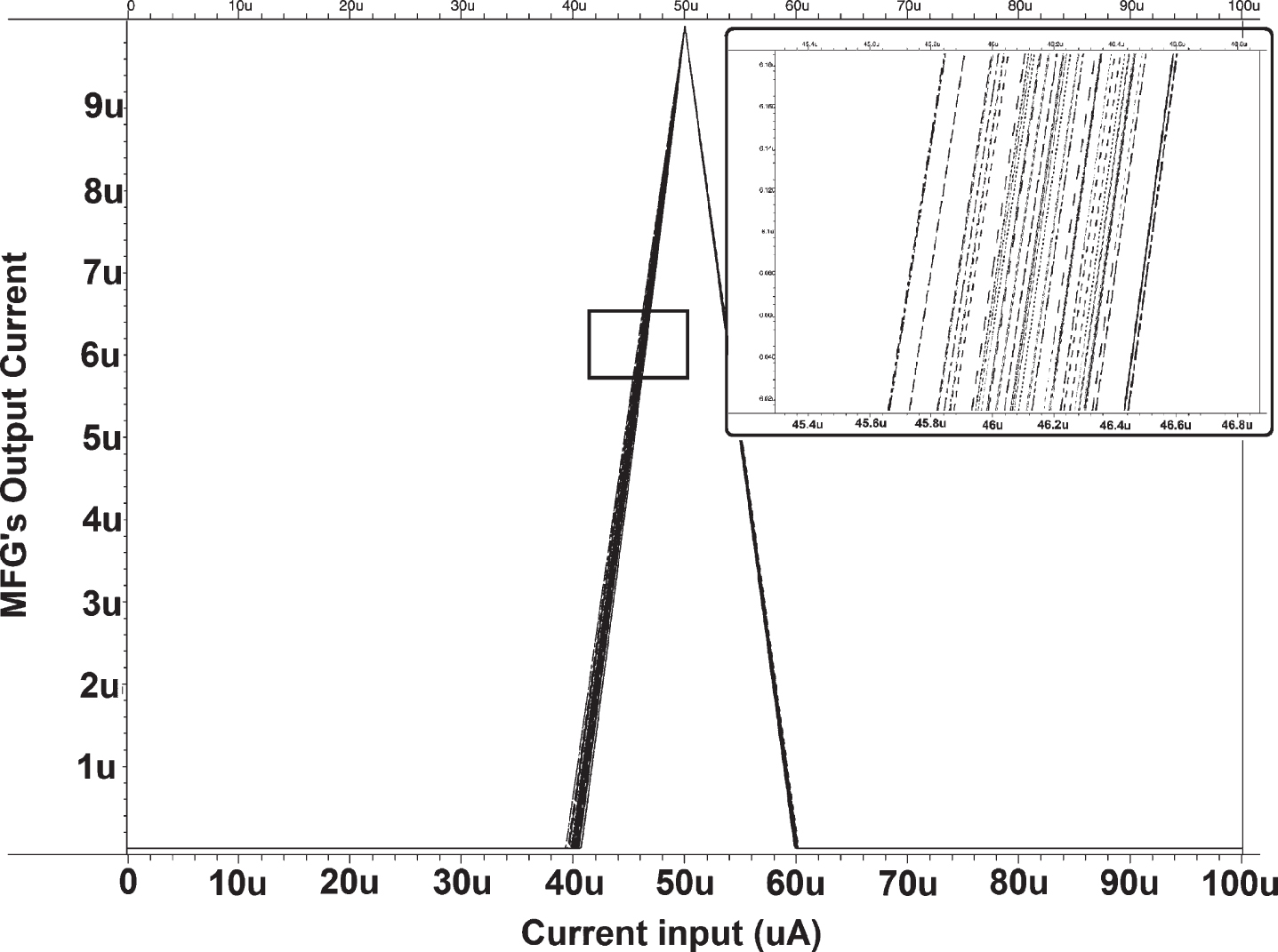
First, we move to the simulation results of the fuzzifier section. As it can be seen in Fig. 7, for a sample trapezoidal output, the upper width of the trapezoid can be changed with the variation in the value of IS.
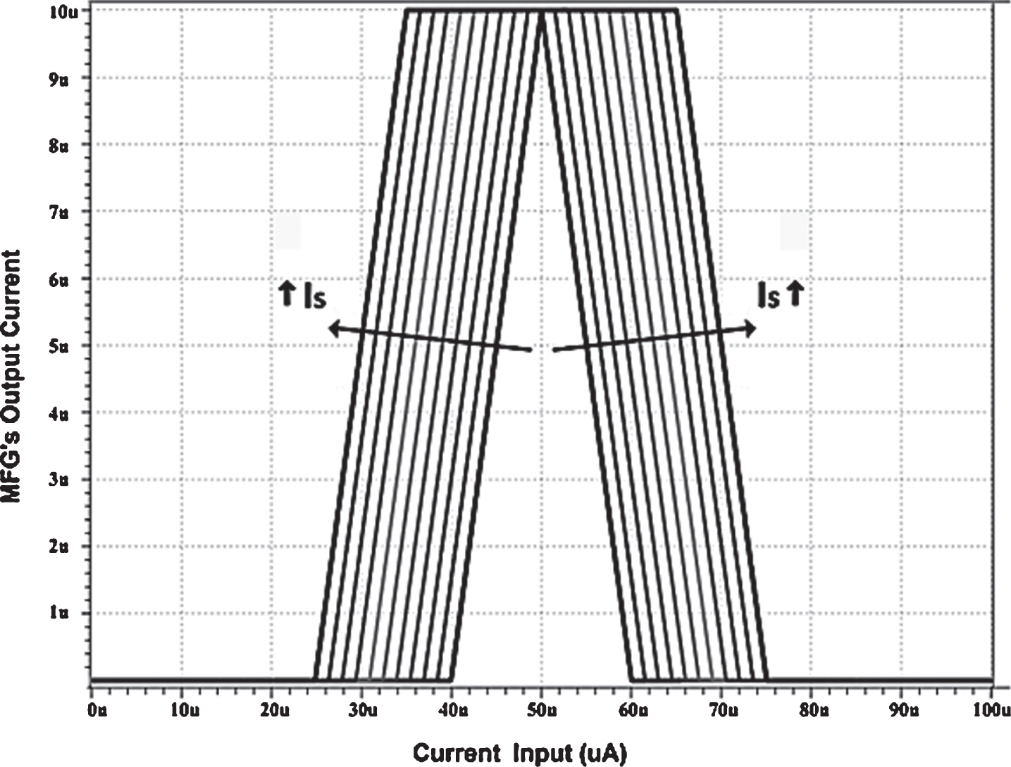
Width altering for a trapezoidal output sample.
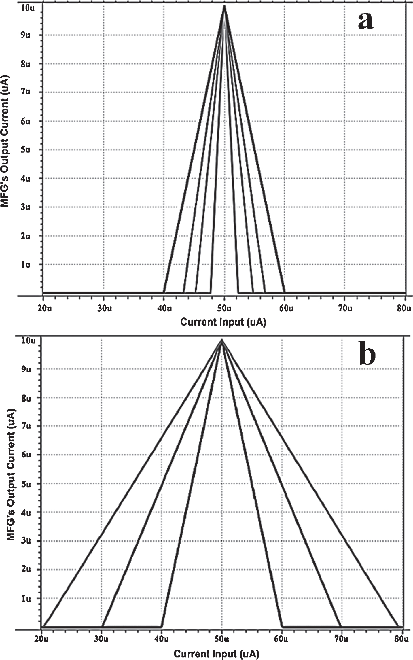
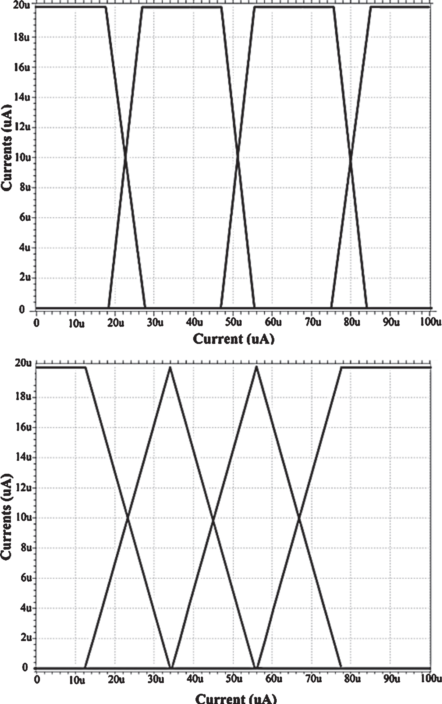
Figures 8a and 8b are S-shape and Z-shape outputs, respectively, in which the starting point of the ramp-like output can be changed by varying the value of Ix.

Changing the ramp-like output’s starting point for a S-shape output and a Z-shape output.
The slope of the ramp-like outputs for sample Triangular outputs can be altered by changing the values of S2-6, which can be seen on Figs. 9a and 9b.
Increasing and decreasing the slope of the waveform for a sample triangular output.
A sample triangular output is shown in Fig. 10 in which the total shape location can be transferred horizontally by changing the value of parameter Ix.
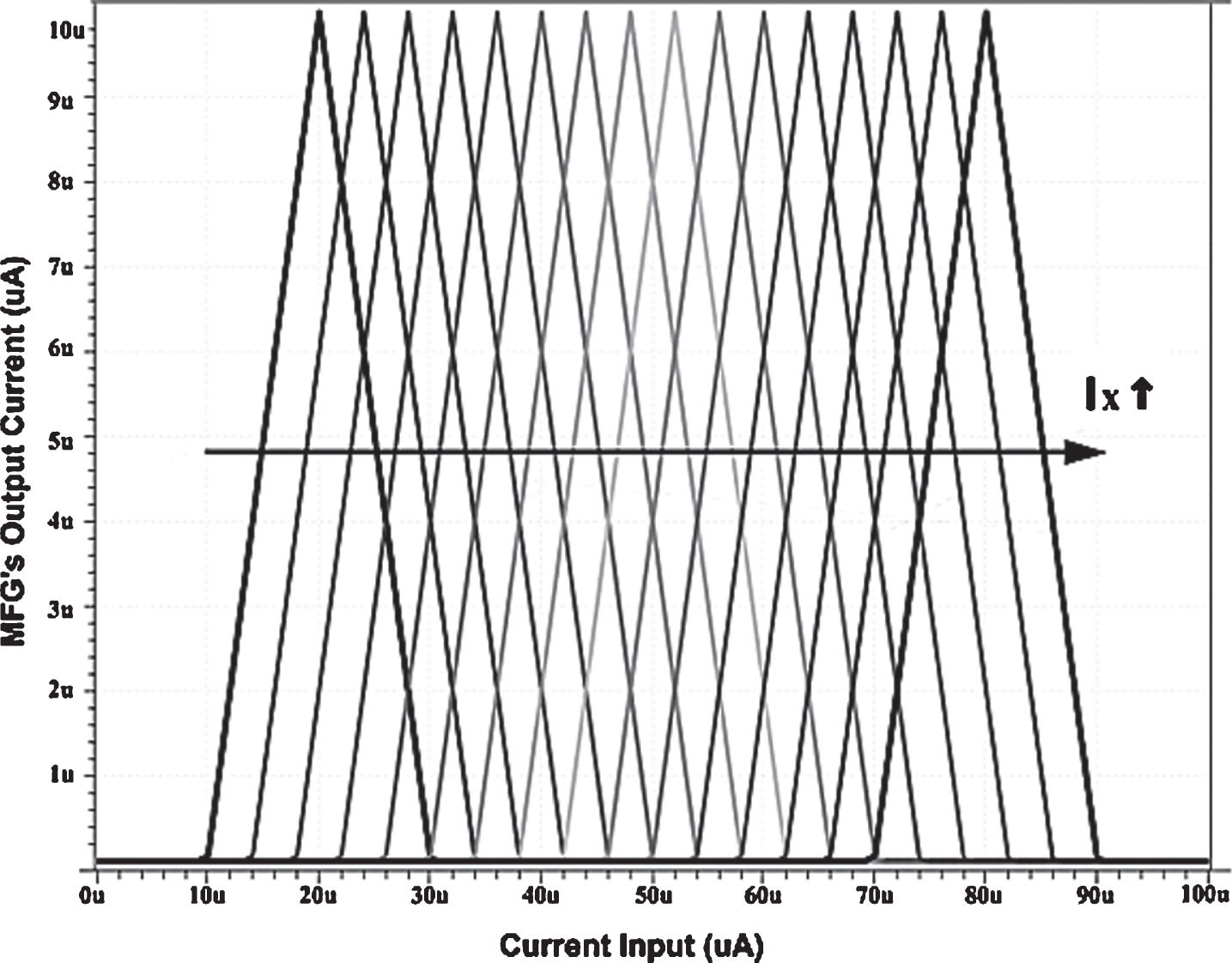
Horizontal transferring of the total shape for a sample triangular output.
To study the effect of small random process variations and device mismatches on circuit behaviour, Monte Carlo simulation is carried out. By assigning random values to the device parameters for each sample of Monte Carlo analysis, a series of results are produced. The proposed membership function has been examined for 50 iterations. Figure 11 confirms that device mismatches do not significantly affect the performance of the circuit.
Monte Carlo analysis.
Power dissipation for the proposed circuit is less than 160μw and it is less than 120μw for most conditions of MFG. The power dissipation for the circuit is shown in Fig. 12 with the parameters below:

Circuit’s power consumption for different values of the input current.
Now, we get your attention to the Min & Max circuit’s simulation results.
Transient analysis with two different types of inputs is accomplished. Sinusoidal inputs with different frequencies and amplitudes are applied to the inputs as I1 and I2, respectively and results are shown in Figs. 13.
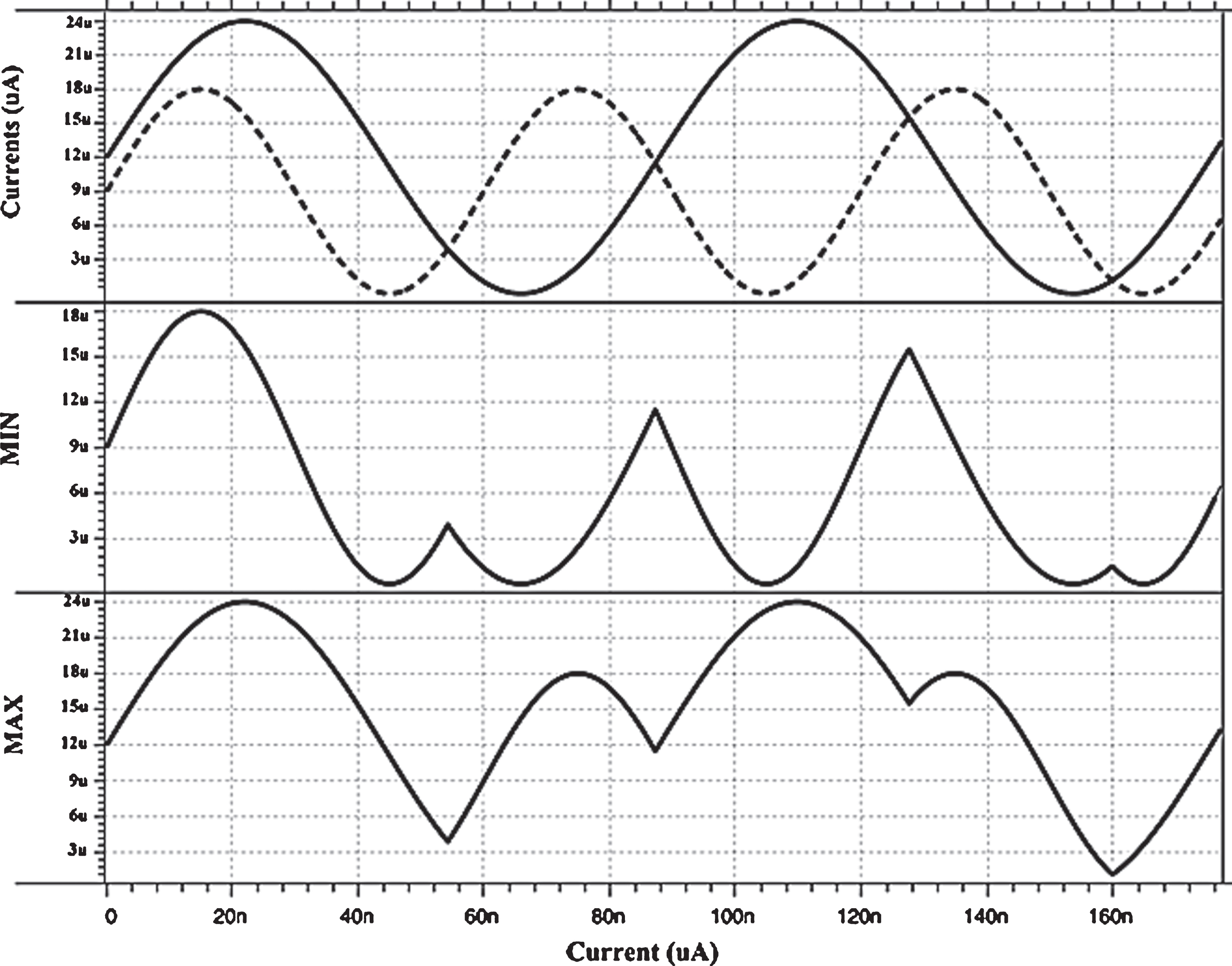
Simulation result of MIN & MAX circuit for two different inputs.
As a conclusion for Min & Max circuit, we can say that high speed and precision are features of the proposed circuit.
This section deals with the simulation of the controller’s total circuit with MATLAB software. The systematic model of controller is analysed with MATLAB software. Two crisp inputs of A and B, in the defined input membership functions model, are assumed to have four language terms (Positive Large, Large, Small and Negative Small) with the shapes as shown in Fig. 14. Figure 15 shows the systematic control surface obtained using MATLAB software.
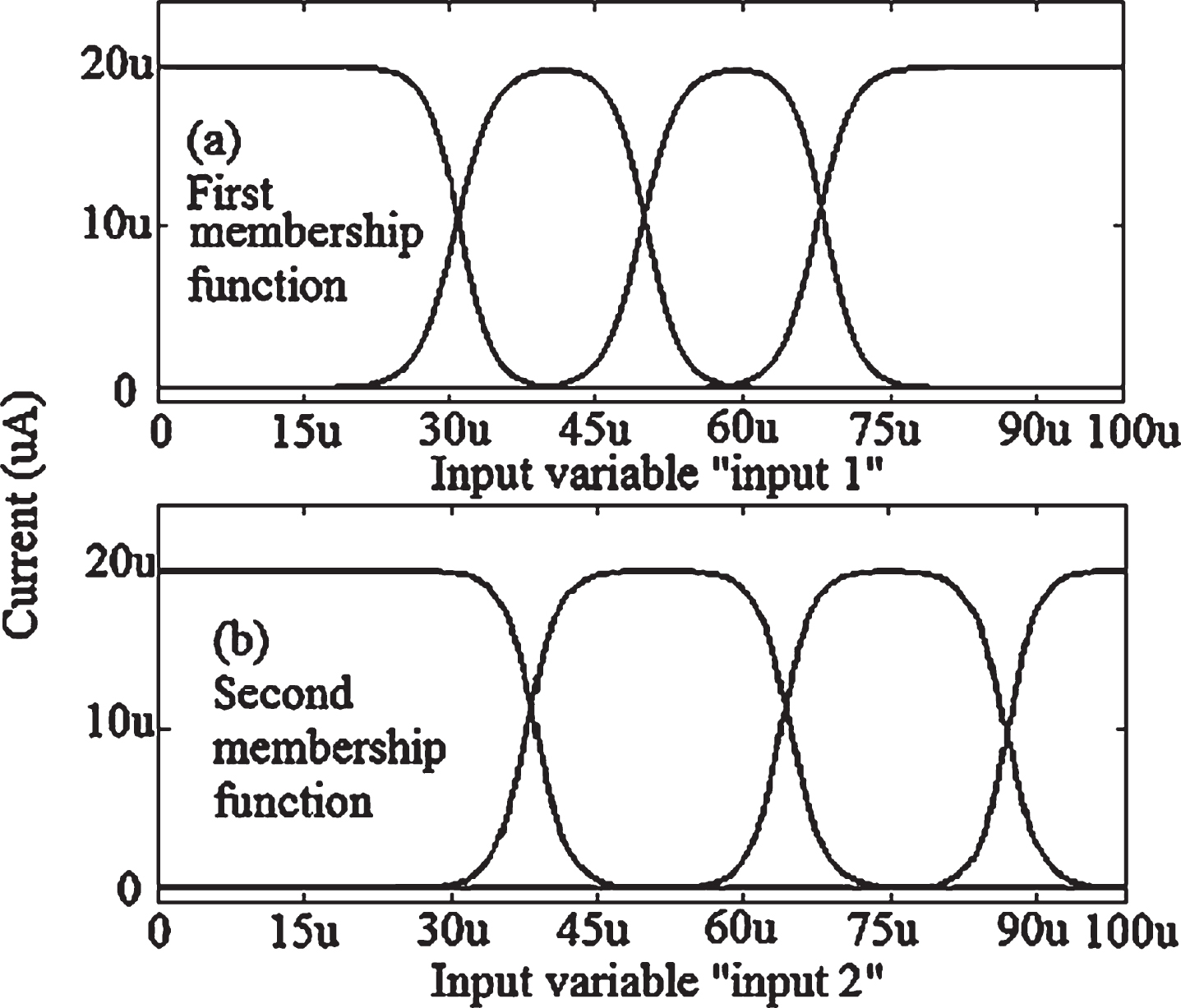
Language terms evaluated with MATLAB.
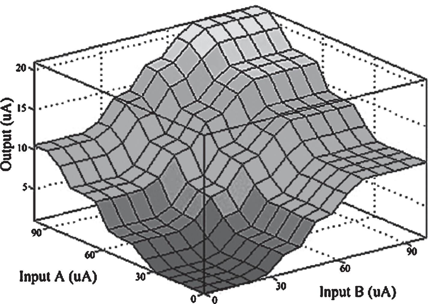
Control surface using MATLAB software.
As mentioned above, the modelled controller is implemented by CMOS transistors in 0.35μm standard technology. The Fuzzifier circuit which is shown in Fig. 2 is used for performing language terms and adapting the results of MATLAB software. The desired membership function is achieved by applying two nunfuzzy inputs of A and B, and setting the current references and digital data which is shown in Fig. 16.
Language terms obtained by Hspice simulation of Fuzzifier circuit (Fig. 2) with setting control data.
Defuzzifier block generates one crisp output varying from 1 to 16 (number of rules) truth value transmitted from the inference block. 16 rules which illustrate the relation between controller’s inputs and outputs are given as follow:
Rule 1: if A is NSA and B is NSB then out is 1uA
Rule 2: if A is NSA and B is SB then out is 3.5uA>
Rule 3: if A is NSA and B is LB then out is 7uA
Rule 4: if A is NSA and B is PLB then out is 10.5uA
Rule 5: if A is SA and B is NSB then out is 3.5uA...
Rule 15: if A is PLA and B is LB then out is 17.5uA
Rule 16: if A is PLA and B is PLB then out is 21uA
Table 2–4 shows a compact of rules with output linguistic terms as singleton that have 7 terms of VVS (Very Very Small), VS (Very Small), S (Small), M (Medium), L (Large), VL (Very Large) and VVL (Very Very Large). These rules are mostly used in different applications especially when inputs are errors and derivation of errors.
Fuzzy rules – linguistic terms
Fuzzy rules – singletons
Fuzzy rules – dedicated numbers
The other simulation result depicts the performance of the ADC. To calculate the FFT we need to have the input data sampled. To do so, as shown in Fig. 17 we put an ideal DAC and ADC to sample the input, before entering to our proposed ADC/Divider. The 64-point FFT graph is drawn in Fig. 18.

The utilized structure to calculate FFT.
The 64-point FFT in corners.
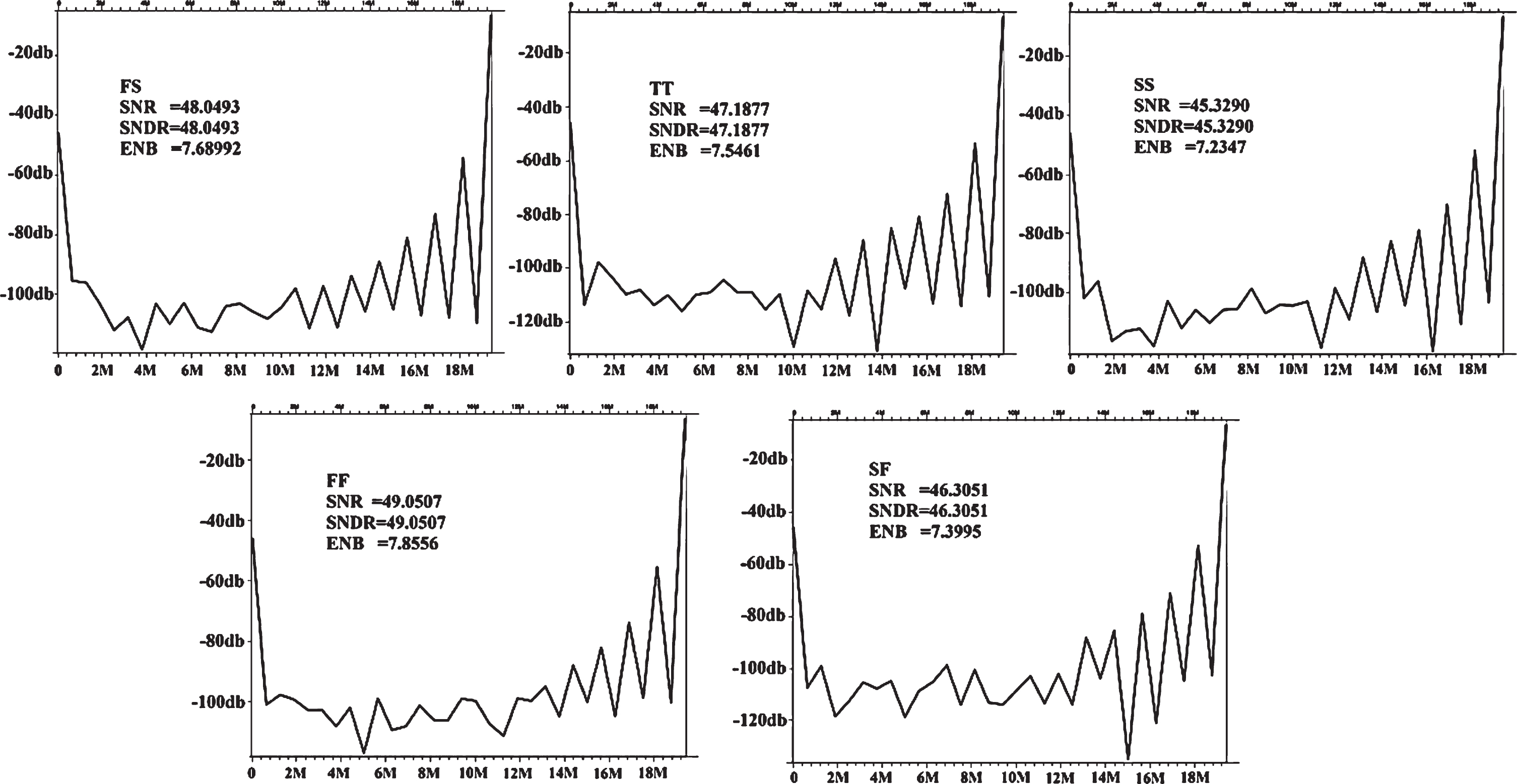
Threshold voltage is one of the most important parameters of CMOS transistors. Nonuniform doping and thin-oxide thickness are the most common variations, both changing the threshold voltage of CMOS transistors. In CMOS integrated circuit designs “TT” stands for typical-typical case and based on the variation of the process parameters there are four corners as follows 0: “SS” corresponds to slow-slow “FF” corresponds to fast-fast “SF” corresponds to slow-fast “FS” corresponds to fast-slow
In each corresponding corner, the first letter refers to NMOS transistor and the second one to PMOS devices. In the fast corner, threshold voltage has the least possible value and the slow corner is the case in which threshold voltage takes its least value. The simulation results of the proposed MFG in different corners are exhibited in Fig. 18.
The presented circuit is designed in such a way that the current does not depend on the absolute value of parameters but on the relative amount of parameters.
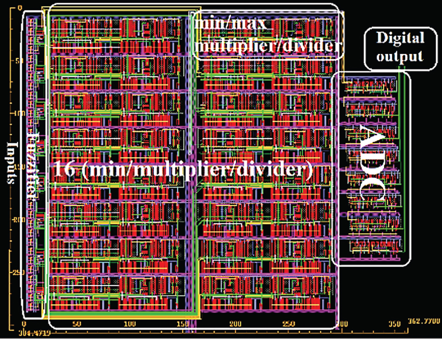
Layout floor plan of the proposed fuzzy logic controller including fuzzifier min/max multiplayer/divider are depicted in Fig. 19 that is implemented in 350μm×300μm effective area. Layout floor plan is generated using the Cadence Virtuoso Layout Plus tool and two poly and four metals in 0.35μm CMOS standard technology.
Layout of the fuzzy logic controller.
After connecting all proposed blocks, the whole system of the controller was simulated using Hspice software in which input A was set as a constant and input B was swept in 16 steps with specific values. According to the results achieved from the simulation, the control system is obtained and illustrated for all combinations of input terms, as shown in Fig. 20. By comparing the control surfaces obtained from Hspice outputs and MATLAB data, it can be seen that there is a good compatibility and similarity between them. The maximum response of controller with applying pulse input is the 23.47 ns delay that results in the 41.3 MFLIPS of inference speed.
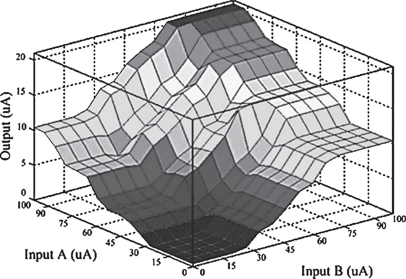
Control surface using Hspice simulation results of extracted layout file.
In the presented article, by using analog circuit realization, there is an enhancement in the inference speed and a capability for employing more accurate defuzzifying methods with the least possible complexity. Producing digital output create a capability for this FLC to support microprocessors and microcontrollers while maintaining the advantages of exploiting analog circuits in basic block of the system. The functionality of this FLC is proved by simulation results of different parts in Hspice and MATLAB. This controller is a two input one output general purpose fuzzy logic controller that can be implemented in less than 0.1 mm2 in 0.35μm CMOS technology. The maximum delay in output is about 24ns that correspond to 41.3 MFLIPS and power consumption is 3.2 mW. The comparison between this fuzzy controller and previous ones is shown in Table 5.
The comparison of proposed controller with previous works
*Post layout. **Post layout + Monte Carlo and corner analyses.