
Abstract
The location attention mechanism has been widely applied in deep neural networks. However, as the mechanism entails heavy computing workload, significant memories consumed for weights storage, and shows poor parallelism in some calculations, it is hard to achieve high efficiency deployment. In this paper, the field-programmable gate array (FPGA) is employed to implement the location attention mechanism in hardware, and a novel fusion approach is proposed to connect the convolutional layer with the fully connected layer, which not only improves the parallelism of both the algorithm and the hardware pipeline, but also reduces the computation cost for such operations as multiplication and addition. Meanwhile, the shared computing architecture is used to reduce the demand for hardware resources. Parallel computing arrays are utilized to time-multiplex a single computing array, which can speed up the pipeline parallel computing of the attention mechanism. Experimental results show that for the location attention mechanism, the FPGA’s inference speed is 0.010 ms, which is around a quarter of the speed achieved by running it with GPU, and its power consumption is 1.73 W, which is about 2.89% of the power consumed by running it with CPU. Compared with other FPGA implementation methods of attention mechanism, it has less hardware resource consumption and less inference time. When applied to speech recognition tasks, the trained attention model is symmetrically quantized and deployed on the FPGA. The result shows that the word error rate is only 0.79% higher than that before quantization, which proves the effectiveness and correctness of the hardware circuit.
Preface
In recent years, deep learning has greatly promoted the development of machine learning technology. Neural networks have been widely used in computer vision [1], natural language processing [2], speech signal processing [3] and other tasks with outstanding performance. The current sequence-to-sequence transformation model is mainly implemented based on the encoder-decoder architecture [4], of which the most popular are fully connected networks [5], convolutional neural networks [6], and recurrent neural networks, such as the long and short-term memory (LSTM) network [7], and the gated recurrent unit (GRU) model [8]). Yet, there is still much room for improving the performance of these models.
When observing an object, the human eyes can quickly capture the most essential features from the massive amounts of input information [9]. Inspired by the research on human vision, the attention mechanism is designed and applied in neural networks, which is so far the most advanced model for solving multi-tasks, such as machine translation, question answering, sentiment analysis, part-of-speech tagging, dialogue system, data monitoring, fault diagnosis [10–15]. The structural model based on the attention mechanism can maintain the spatial map and measure the importance of different features based on the corresponding weights. By judging the relevance of features, the model establishes dynamic weight parameters to strengthen critical information and weaken irrelevant information, which enhances the efficiency of deep learning algorithms and meanwhile, address the shortcomings of traditional deep learning [16]. In addition, the attention-based models overcome some limitations of traditional neural networks, such as decreased performance decreasing with the increasing input length, overdependence of the computing efficiency on the sequence of input as well as poor capacity for feature extraction and enhancement [17]. The attention mechanism can be employed to model sequence data of random lengths, which further enhances its ability to capture remote dependent information, reduces the depth of layers, and improves accuracy [18]. According to the differentiability of the attention mechanism, it can be divided into hard attention [19] and soft attention [20]; With regards to the attention domain of the attention mechanism, it can be divided into spatial domain [21], channel domain [22], layer domain [23], mixed domain [24], time domain [25] and other different types. Among them, the location attention is a commonly used method, which, with its efficient and concise calculation method, can be used to capture the positional relationship of timing signals [26]. In the applications where the location of the decoded information is highly correlated, such as speech recognition [27, 28] and machine translation [29], the location attention mechanism can effectively improve the performance of the models.
In order to embed a high-performance deep learning inference model into the device, it needs to be implemented in hardware. CPU is not suitable for intensive parallel computation as it has few computing units and cache units [30]. On the contrary, GPU has many computing units, which is generally suitable for heavy and parallel computation. It runs faster but consumes more power, especially in the inference step, than CPU. Due to the limitation of the amount of data, GPU cannot make the fullest of its advantage in computing speed enabled by its high bandwidth and multiple computing cores [31]. ASIC chips are generally only suitable for certain types of algorithms, and when the algorithm changes, ASIC cannot handle it iteratively [32]. The field-programmable gate array (FPGA) boasts many advantages as a high-performance programmable chip: low power consumption, small size, high integration, fast speed, short development cycle, low cost, user-definable functions, reprogrammable programming, and erasing. In recent years, FPGA has become a key component of high-performance digital signal processing systems in digital communication, voice, video, and image processing. The logic structure of FPGA includes look-up tables, registers, multiplexers, memories, fast adders, multipliers, and I/O processing dedicated circuits. FPGA can implement high-performance parallel algorithms and is ideal for forming a high-performance customized data processor [33]. FPGA is more suitable for the hardware implementation of the location attention model which requires a higher inference speed and more power consumption.
Recurrent neural network and convolutional neural network are the core computing units for processing sequence and image data respectively, and the corresponding activation function and batch normalization layer also play an important role in neural network calculation. Therefore, there are a large number of accelerators implemented by FPGA and ASIC [42–45]. By integrating different operators, many classical deep learning algorithms have been deployed on FPGA and ASIC. For computer vision, there are CNN based target detection models [34], real-time online face detection models [35], real-time target segmentation models [36], etc. For speech signal processing, there are RNN-based automatic speech recognition models [37], microphone array-based speech enhancement models [38], signal processing-based speech noise reduction models [39], etc. For natural language processing, there are English corpus translation system [40], word vector embedding model [41], etc.
In order to improve the inference accuracy of neural network, we need to introduce attention mechanism and implement it. However, the computational process of attention mechanism not only requires quantities of matrix multiplication and vector multiplication, but also occupies a lot of computational consumption, which limits the acceleration of neural network model. At present, there is little research on the hardware circuit of attention mechanism module, because attention mechanism, as a computing idea, has various structures in different networks and applications, for example self-attention in transformer [9]. The attention mechanism is embodied in a large number of vector multiplication and matrix multiplication operations in hardware, that is, the matrix multiplication accelerator is stacked [49]. But the traditional vector multiplication accelerator can only ensure the correct function of matrix multiplication in attention calculation, and can not achieve the optimal acceleration effect in the face of the massive information flowing through the attention module, such as matrix multiplication accelerator [50]. There are fewer hardware accelerators dedicated to attention mechanism than CNN and RNN accelerators. A3 use approximate calculation instead of enumeration search to reduce the calculation cost, and improve the calculation performance through algorithm pipelining [51]. In [47], two hardware resource sharing modules, the multi head attention (MHA) Resblock and the position wise feed forward network (FFN) Resblock, are designed for the transformer to solve large matrix operations in the transformer through efficient segmentation methods. The FTrans enhancement module block circular matrix (BCM) - based weight representation compresses large-scale language models from the algorithm level and realizes hardware acceleration [48]. FPGAN uses the method of software and hardware coordination design to accelerate the FPGA of graph attention networks, and eliminates the use of DSP by using shift addition instead of multiplication accumulator [46].
The above design focuses on two directions: algorithm compression model and hardware optimization of computing resources, but less hardware optimization design from the perspective of algorithm computing characteristics. Attention mechanism is based on the similarity of vector content to search the dynamic weight. This search process is reflected in the hardware that the sequence data continuously flows through the fixed weight matrix. Based on this computing feature, we design a full pipeline structure for the attention module, and make the hardware computing module share and reuse through the integration of algorithm and structure. Finally the high-speed transmission of sequence data through the attention module and streaming computing are realized.
The main contributions of this paper are as follows: Given the high computation cost and colossal storage requirement of the location attention network, fully connected layers FC1 and FC2 share weight storage space and calculation array. To address the problems of dramatically increased demand on hardware resources and limited design for hardware pipeline when the convolutional layer and the FC3 fully connected layer are executed separately, we implement the algorithm with a single fully connected layer Inc by merging the convolutional layer and the FC3 layer, which shares the computing array with the FC1 and FC2. By precise pipeline timing and parallel data flow scheduling, a shared computing architecture and parallel computing array are implemented. With efficient computing processes, it can significantly reduce the amount of data transmission, hardware computing resources, and storage resources, and thus, the acceleration of the FPGA-based location attention mechanism can be achieved.
Location attention mechanism
The seq2seq model based on the encoder-decoder structure has been used widely. However, the decoder lacks a mechanism to tag the relevant input when outputting each token. The attention mechanism introduces attention weights in the encoding sequence so that different input tags can be given different degrees of attention and improve the quality of output tokens.
Taking the location attention mechanism implemented by hardware in this paper as an example, the encoder first performs encoding calculation on the input sequence vector and obtains t time-length and dimension p encoding vectors. When using decoders such as LSTM to decode the encoding vector, each decoding step needs to take care of the different parts of the encoding vector. The weights of different time steps are calculated through the location attention network and merged to obtain the context vector
In a typical location attention network (as shown in Fig. 1), the encoding matrix

The location attention mechanism.
Parameters of the location attention-based neural network
Given computing resources, storage resources, and algorithm flow, we have adopted three design methods in the hardware circuit: layer fusion of convolutional layer and fully connected layer, shared computing architecture, and parallel computing array, which have improved the computational efficiency of the hardware circuit.
Layer fusion of convolutional layer and fully connected layer
In neural networks, the convolutional layer is usually used to extract local abstract features from feature maps, and the fully connected layer is used to learn a particular functional mapping relationship from the feature maps, these two layers are designed for different processing goals. However, both layers are essentially matrix multiplication and accumulation operations from the perspective of hardware computing, so in our location attention mechanism, we fuse the adjacent convolutional and fully connected layers to form a relatively simple, fully connected layer. This can simplify the iterations of the algorithm, improve parallel pipeline, and accelerate hardware.
Fusion method
The attention weight vector
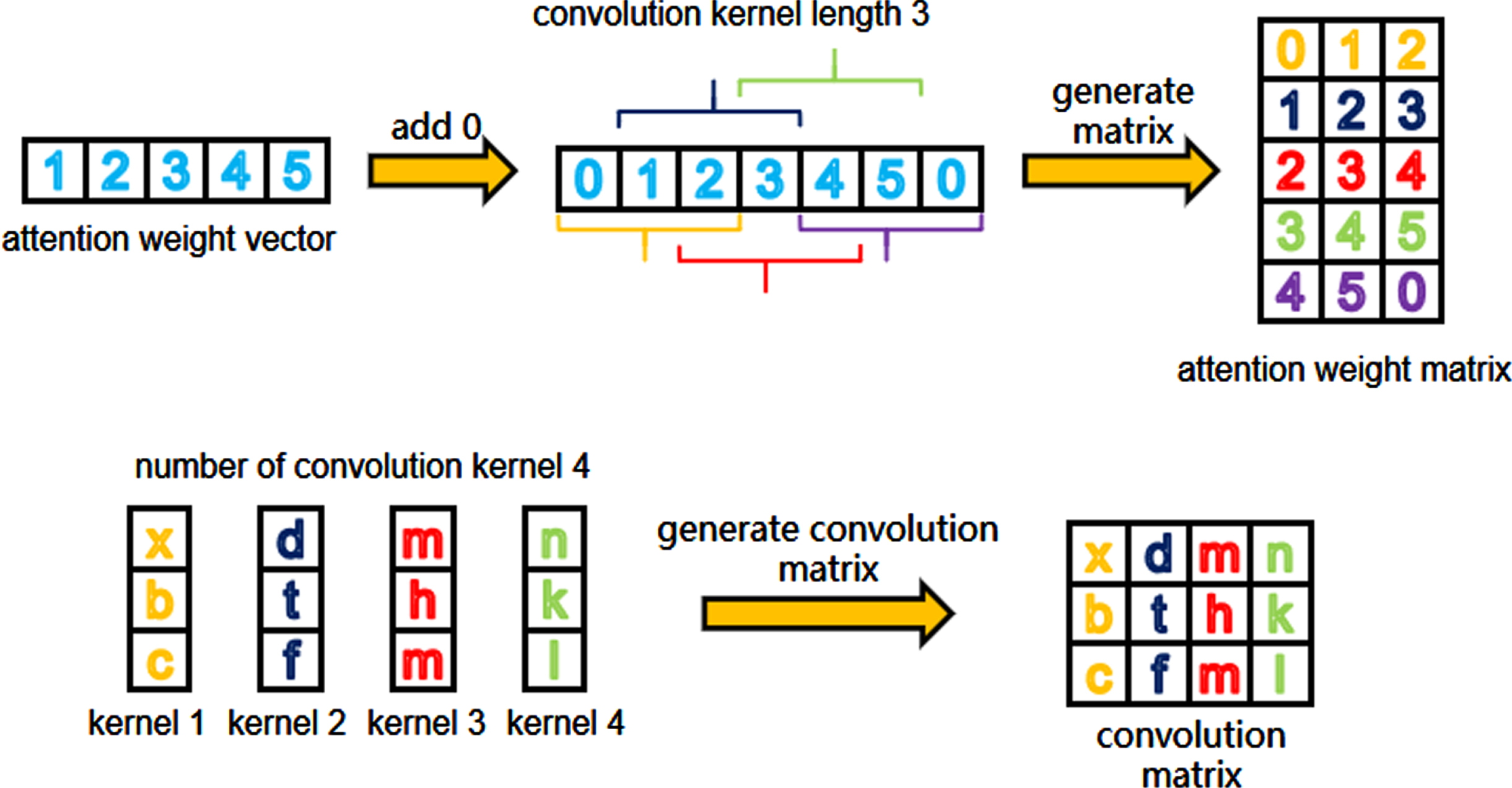
Schematic diagram of attention weight vector and convolution kernel conversion.
In this subsection, a theoretical analysis and comparison on the computing resources and performance of the hardware before and after the fusion of the convolutional layer and the fully connected layer is presented
Generally speaking, multiplication of 2 matrices with dimensions of a × b and ×c, respectively, requires a × b × c multiplications and a × b × c additions, thus, for unfused continuous convolutional, fully-connected layers, a total of t × l × n + t × n × m multiplication and addition operations are required. As for hardware, the attention weight vector
When l is small while m and n are large, a high degree of parallelism (large p
n
and p
m
) is required to meet the pipeline timing requirements. If the above timing requirements are not met, the total execution time required to complete the two calculation segments is t × l × n/p
n
+ t × n/p
n
× m/p
m
; if the timing requirements are met, the total execution time is about t × l × n/p
n
+ n/p
n
× m/p
m
, the total computing resource usage is p
n
+ p
n
× p
m
, and the throughput rate is p
m
/l. The higher the degree of parallelism, the shorter the execution time, and the greater the utilization of computing resources. Therefore, it is necessary to comprehensively consider performance and resource utilization and choose p
n
and p
m
as a compromise. In addition, in the case of ignoring the consumption of input and output buffers, only matrices
When the continuous convolution and fully connected layers in the location mechanism are merged, the two layers are simplified into a single fully connected layer Inc. The hardware only needs to calculate
Comparing the performance before and after the fusion, we observed that ➀ When the algorithm dimension parameters are determined, the hardware computing resources and performance after fusion are only affected by one parallelism parameter p m ; ➁ The throughput rate before and after the fusion is the same; ➂ Under the exact parallelism, The hardware computing resources required after the fusion are less than those before the fusion; ➃ The pipeline sequence after the fusion has no violation constraints; ➄ When n/p _ n = m/p m , the calculation time before and after the fusion is almost the same.
In summary, when the number of convolution kernels n is large, and the output feature dimension m of the fully connected layer is small, the fusion mechanism can reduce the number of multiplication and addition operations. Even if the algorithm dimension does not meet the conditions for reducing the number of operations, this fusion mechanism can significantly improve the algorithm’s parallelism and the parallelism of the hardware pipeline. The fusion mechanism can reduce the consumption of hardware computing resources, simplify the calculation process, reduce the complexity of circuit pipeline design, and use the maximized parallelism to achieve the same computing performance as before the fusion. Although the weighted storage resource usage and total calculations do not have an advantage, using FPGAs’ rich resources and 512 parallelisms, hardware calculations can meet the exact computing power requirements. Meanwhile, the multiply-accumulate structure can also time-share computing resources with the other two algorithm blocks.
Shared computing architecture
Shared computing architecture design method
In the location attention mechanism implemented by hardware in this paper, fully connected computing FC1, FC2 and the fusion layer (Inc) dominate the amount of calculation. According to the inference process of the seq2seq model based on the location attention mechanism, the encoder no longer participates in any operation after completing the calculation of the encoding vector, and the encoding matrix
Based on the design idea of FC1, FC2 and Inc sharing computing arrays, the attention mechanism circuit module is mainly composed of computing arrays, storage modules, and control circuits, as shown in Fig. 3. The input vector is directly sent to the calculation array via the external buffer, and the data path of the weight and calculation result is connected with each local storage module. The Inc convolution process is different from the fully connected calculation. The data flow from the external bus into the shift register conv_fifo module through the buffer, and after the data stream is processed, it is sent to the calculation array, and the multiplication and accumulation calculation is performed. The storage module has the right to re-storage module (WRAM*) and intermediate result storage module (FC*_Res_RAM). WRAM0 is used to store the weight of the fully connected calculation module FC1 or FC2, WRAM1 is used to store the weight of the Inc, and WRAM2 is used to store the weight of the fully connected calculation module FC4. FC*_Res_RAM stores the calculation results of FC1, FC2, and the convolution module, respectively, and FC3_Res_RAM uses a ping-pong storage mechanism. Table 2 lists the scale of each storage module, and the total storage capacity is less than 1MB.

Location attention mechanism circuit structure diagram.
Storage usage of location attention mechanism circuit module
The circuit of the attention mechanism adopts a resource-sharing design. FC1, FC2, and convolutional calculation share the computing array, and FC1 and FC2 share the weight storage module WRAM0. The entire attention mechanism circuit guides the control circuit through the instruction stream sent from the outside and realizes three kinds of data scheduling so that the circuit realizes three kinds of calculation functions in different calculation stages. The three data flows are shown in Fig. 3 (➀ FC1 calculation process; ➁ FC2 calculation process; ➂ Inc calculation process). By designing this hardware data stream transmission and calculation, the data stream transmission time and calculation time in the decoding process can be reduced. The specific process is shown in Table 3.
Hardware execution process
In the hardware circuit of the location attention mechanism, there are: FC1 Layer: the input data volume is t×512, the weight data volume is 512×512, and the calculation volume is t×512×512; FC2 layer: the input data volume is 1024, the weight data volume is 1024×512, and the calculation amount is 1024×512; Inc layer: the input data volumn is t, the weight data amount is 256×512, and the calculation amount is t×256×512.
Since the fully connected calculation FC1 is only calculated once in the entire decoding process, meaning that steps 1 to 6 are executed only once, which significantly reduces the number of calculation units and the weight retransmission time. Specifically, in the decoding process after the first round, the FC1 calculation amount is reduced by t×512×512, and the weight transmission reduction is 512×512 + 1024×512 + 256×512. The actual transmission data amount per round of decoding is only 1024+ t, the hardware circuit only needs to perform calculations for FC2 and Inc. Due to the three computing functions sharing a computing array, the actual usage of computing resources is reduced 1/3 of the demand.
Parallel computing array
According to the previous pipeline analysis, when p _ m = m maximizes the degree of parallelism, the hardware can obtain the best computing performance, and the computing array of the attention mechanism circuit module is arranged in parallel with 512 computing units (PE). The 512 PEs are controlled by a synchronous control circuit, which independently completes multiplication and accumulation calculations, and the peak calculation capacity of the calculation array reaches 1024 OPS/clock. Each calculation unit is a multiply-accumulator composed of an 8-bit×8-bit multiplier and a 32-bit adder. According to the data characteristics of the algorithm, 512 PEs share the same input sequence and obtain different calculation results by receiving different weights. Therefore, when the input vector connected to the calculation array adopts 8-bit channels, and the weights and calculation results adopt 4096-bit channels, the calculation array can receive 512 weights at the same time, perform 512 multiplication and addition operations per beat, and outputs 512 data.
Based on the described calculation array structure and interface, the throughput rate of the calculation array is determined by the accumulation depth. The accumulation depth of FC1 is 512, the accumulation depth of FC2 is 1024, and the accumulation depth of the Inc layer is 256, thus, the throughput rates are 1, 0.5, and 2, respectively. FC1 and FC2 can flow 512 calculation results into the intermediate result buffer at a rate of one data per beat in the throughput gap, according to which the output interface bit width is set to 8 bits. Since the Inc layer’s cumulative depth (256) is smaller than the parallel width (512), to output 512 data per 256 beats, the output interface must output at least 2 data per beat on average. For this reason, the scale of the calculation module after Inc has been doubled. Two sets of accumulation, tanh and PE circuits, are set up to execute in parallel. After the above-mentioned precise parallel pipeline design, the computing array can be calculated at full speed with the peak computing power of 512 MAC/clock, and the intermediate results are transmitted simultaneously. After the Inc layer, the accumulation, tanh, and multiplication accumulation operations are all hidden in the array calculation process.
Hardware circuit design
The overall hardware circuit design diagram of the location attention mechanism is shown in Fig. 4. The parameters, control, and status information are transferred to the control, status, and local registers through the parameter interface, and the data bit width is 32. The interaction of the register and the global control module can operate the entire hardware circuit. The attention core module is the core calculation circuit, which handles the complete calculation process of the location attention mechanism, in which data such as feature maps and weights enter the calculation core in a data stream through the bus, and its data bit width is 256.

Location attention mechanism circuit structure diagram.
After the neural network model has been trained on GPU, in order to make rapid inference on the FPGA, we need to compress and quantize the trained model, that is, convert the float32 floating-point storage (operation) to integer int8 storage (operation) and control the accuracy loss within a specific range.
The entire location attention mechanism module mainly includes a fully connected layer and a convolutional layer, and we use the same quantization method for the convolutional layer and the fully connected layer. Taking the fully connected layer as an example, the quantitative relationship of the relevant data of the network layer is as follows:
Neural network quantization generally causes losses to the accuracy of the original network. To obtain the optimal quantization coefficients for minimizing the quantization error of the neural network, we use TensorRT to solve the optimal quantization coefficient. For the weight quantization coefficient S w , TensorRT uses the method based on the maximum symmetric interval mapping to solve, namely:
In this formula, p (x) and q (x, S x ) represent the distribution of data before and after quantization. In the hardware circuit design, the weight data Q w and the feature map data Q x and Q y are set to be 8 bits, and the offset data Q b bit width is set as 32 bits, and thus, the bit width of the calculation result of Q w × Q x + Q b is 32 bits. In order to make the input and output data bit width of the calculation circuit consistent, the weight quantization coefficient and the feature map quantization coefficient are solved first, and Q w × Q x + Q b is multiplied by S w × S x /S y , so that data bit width is converted to 8bit, which unifies the input and output bit widths of the calculation circuit.
Experiment
Experimental setup
For the location attention mechanism circuit described in this work, we use the quantization method described in section 3 to quantize the neural network feature and weight data into 8bit, then use Verilog hardware description language to design and implement it on the Xilinx FPGA development kit ZC706. The FPGA chip model used by this development board is xc7z045ffg900-2.
We verify the proposed design method from four aspects. Firstly, the resource consumption of FPGA circuit is counted, and the calculation time of each step is analyzed; Then, the inference speed and power consumption are compared with other hardware implementation platforms such as CPU and GPU; Then we compare the comprehensive performance of hardware resources, frequency, power consumption and other aspects with other FPGA implementation methods of attention mechanism; Finally, its actual performance in speech recognition application scenario is verified.
Resource consumption and calculation time
According to the statistics on the use of FPGA hardware resources, the entire hardware implementation uses a total of 2 DSPs; 61135 and 42606 look-up tables and registers are used respectively, of which the computing array accounts for the primary usage; the block storage RAM is 201.5, which mainly occupies Store in weight. In a real case, the circuit adopts IP core encapsulation, and the data interface and parameter interface adopt AXI-4 protocol, respectively: its data interface adopts the bust transmission mechanism, and CDMA control data is transmitted between the IP core and on-chip storage. The central processing unit ARM or MicroBlaze controls the system-on-chip and configures and controls the IP core through the parameter interface. The parameter interface includes a control register, a status register, and 6 parameter registers. The central processing unit controls the registers and initiates data transmission and calculation operations at different stages in the form of pulses. Furthermore, it reads the status register and monitors the running status of the circuit in real-time according to different status bits. Therefore it can interact with the attention mechanism IP core.
The data transmission waveform and calculation time of the location attention mechanism circuit are shown in Fig. 5 and Table 4. The vector transmission and calculation time of FC1, the weight transmission time of FC2, and the calculation time of Inc account for the primary time consumption. However, the actual decoding process of FC1 vector transmission and calculation, FC2 weight transmission, and Inc weight transmission is only performed once, so the primary time consumption is in the calculation process of Inc, the execution time of the decoding process is about 338 us at a clock frequency of 100 MHz. According to the calculation dimension relationship, the calculation time of Inc is proportional to t. The more decoding rounds, the smaller the ratio of steps ➀ to ➅ occupying the total execution time. When the decoding round reaches dozens of times, steps ➀ to ➅ can be ignored, and when t is large, the total execution time is dominated by t.

Attention mechanism circuit transmission waveform diagram.
List of execution time (t = 128, fclock = 100Mhz)
In order to compare the implementation results of different hardware devices, the location attention mechanism have been run individually on the CPU, GPU, and FPGA for multiple times, the performance of which are compared in terms of their average inference speed and power consumption. The speech recognition task is performed based on seq2seq as a test case. First, the location attention mechanism is implemented in python 3.6 language, the software operating system is Ubuntu 16.04, and the deep learning framework is PyTorch 1.4. Then, 2000 voice samples were randomly selected as the test sample set in the AISHELL-1 public data set, and the operation time of the location attention mechanism was calculated using the python time library. By setting the device attributes of the tensor and model in PyTorch, it can run on the CPU or GPU, respectively.
In this test, the CPU device is Core i7 k7700, the primary frequency is 4.2 GHz, the third-level cache is 8MB, and the number of cores is 4; the GPU device is NVIDIA GeForce GTX 1080Ti, the memory capacity is 11264MB, the core frequency is 1480 MHz, and it contains 3584 stream processors. The power consumption of location attention mechanism FPGA circuit is shown in Fig. 6 and the experimental results are shown in Table 5.

Power consumption of attention mechanism circuit.
Performance comparison of Location attention mechanism on CPU, GPU and FPGA
For different FPGA implementation methods of attention mechanism, their hardware resource consumption and overall performance are different. We choose FPGAN [46, 47], Ftrans [48] as the control to compare the performance from three aspects: hardware resource usage, power consumption and computing time. The results are shown in the Table 6.
Comparison of hardware resource consumption, inference time and power consumption
Comparison of hardware resource consumption, inference time and power consumption
The comparison results show that our hardware uses very few hardware resources compared with other designs, which is due to our hardware sharing design, so that different computers can share the same hardware resources. Because the pipeline design is adopted and the calculation process is reasonably designed to reduce the consumption of data transmission, the execution speed of our design method is second only to [14]. Power consumption we measure is on-chip power consumption. Other hardware may provide board level power consumption, which cannot be directly compared.
To verify the actual inference performance in the FPGA hardware circuit of the location attention mechanism, the automatic speech recognition task was performed in our experiments.
First, the seq2seq model based on the location attention mechanism is still based on the pytorch framework. For any speech sample with a sampling rate of 16 kHz, each frame is represented as an 80-dimensional vector using the MFCC feature extractor, where the frame length is 25 ms, and the frameshift is 10 ms. The encoder part is a 5-layer BiLSTM structure (the state vector dimension is 512). At the same time, in order to effectively reduce the length of the speech sequence, we set a drop sampling mechanism (discard the former of the two state vectors and retain the latter) in the second, third, and fourth layers, as shown in Fig. 7. Decoder network is LSTM (the dimension of the state vector is 1024). It accepts the encoding result as input and outputs one character at each time step until the end character appears. When decoding at each time step, it is necessary to obtain the output character of the previous step and the context vector obtained by the attention mechanism. The scale of the vocabulary depends on the training data set, and the dimension of the embedding word vector is set to 512, as shown in Fig. 8; the parameters of the location attention mechanism are shown in Table 1.

Encoder structure diagram.

Decoder structure diagram.
To verify our proposed design, different-scaled, public data sets in 4 languages such as AISHELL-1, AISHELL-2, CSJ, and Switchboard were used to train the seq2seq model, and the model was quantified using the quantification approached described above. For comparing the accuracy of the location attention mechanism, the model’s encoder and decoder were run on the CPU, and test speech recognition on different test sets on GPU (unquantized), GPU (quantized), and FPGA, respectively, to achieve recognition error rate that are shown in Table 7.
Test results of seq2seq model using Location attention mechanism
Experimental results show that when the model is quantized and compressed, the accuracy will be reduced to a certain extent due to the conversion of floating-point numbers to fixed-point numbers. When the quantified model is deployed on the FPGA, its inference accuracy remains consistent, which verifies the correctness of the hardware circuit. The experimental results also show that the automatic speech recognition model using the attention mechanism implemented by FPGA hardware remains within a certain accuracy level.
Considering both algorithm performance and hardware implementation, we propose an efficient inference circuit design for the location attention mechanism and its FPGA based hardware implementation. The main features can be concluded as follows: (1) Three circuit designs are proposed, i.e., layer fusion of convolutional layer and fully connected layer, shared computing architecture, and parallel computing array, which can effectively reduce the consumption of hardware resources and accelerate the pipeline parallel computing of the attention mechanism. (2) Compared with the performance of different hardware platforms, the inference time of the hardware circuit based on FPGA is 0.010 ms, which is about a quarter compared to that using GPU, and its power consumption is 1.73 W, which is about 2.89% in comparison with CPU. (3) Compared with other FPGA implementation methods of attention mechanism, the hardware circuit we designed uses less hardware resources, which shows the effectiveness of the shared computing array design method; In addition, our method also achieves faster reasoning speed, which shows the effectiveness of computational flow optimization and pipeline design; (4) In the actual task of automatic speech recognition, the trained model is quantized and deployed. In different public data test sets, the word error rate increases by an average of 0.79% compared with that before quantization, and the final word error rate is within an acceptable range. To sum up, the location attention mechanism hardware module we designed has three characteristics: high performance, low power consumption and fast reasoning speed, which can provide a very excellent solution for the key module location attention mechanism in the current speech recognition hardware acceleration problem.