
Abstract
Fabrication of semiconductor wafers is a complex process and chances of defect wafers are high. Because of defective wafers the circuit patterns will not be created correctly and it is necessary to identify them. Manual identification of defects are time consuming and expensive. Deep learning methods are widely used for defect detection. In this paper we propose a simple Convolutional Neural Network (CNN) model for classification of nine defects in wafers. A custom CNN consisting of 9 layers is used for the classification of defects as Center, Donut, Edge-Loc, Edge-Ring, Loc, Random, Scratch, Near-full, and None. Performance of the model is evaluated using WM-811K dataset. Results shows that the model classifies the defects with high confidence score and an accuracy of 99.1% is achieved using this method. Further, the convolution operation in the CNN is realized using Coordinate Rotation Digital Computer (CORDIC) algorithm. The model is implemented in Field Programmable Gate Arrays (FPGA) and proved less complex method and consume less computational power than conventional methods.
Keywords
Introduction
Nowadays, technology is evolving to serve its customers. Semiconductors are an important component employed by artificial intelligence, 5G, smart devices, the Internet of Things etc. Semiconductor gadgets are built on a sequence of nano-synthetic processes made on substrates made of a single pure silicon crystal and these substrates are commonly referred to as wafers. The fabrication process is very tedious, costly and multiplex. Preparation of wafer is the first step in the making of IC. It involves cutting, shaping, and polishing the wafer pieces to make them suitable for further processing. Some wafers need to be adjusted to be convert to the required wafer because of their choppy floor, uneven surface and shape. But semiconductor engineers even though working with high quality devices in a clean surrounding, cannot bring out error-free wafers [1]. Technological advancements have enabled semiconductor refining, resulting in tremendous expansion in the industry [2].
The defects will be having particular reasons and correct classification help to focus on the issue and solve them [3]. There are many defect failure patterns. Center, Donut, Edge-Loc, Edge-Ring, Loc, Random, Scratch, Near-full, and None are the defect types. Each one of these deformity pattern types can provide process engineers with critical production process information. Center patterns, for example, may be caused by a uniformity issue during synthetic mechanical planarization. Donut is a kind of ring defect. It will be soft bake after photoresist development. The centre of the wafer becomes less defective at the time of the rinsing phase. Edge-Local defect is due to regional fault at the wafer’s edge caused by uneven thermal treatment during the Diffusion stage. The ring-shaped fault around a wafer is known as an edge-ring. It is because of improper temperature control during the high-speed thermal treatment phase, as well as anomalous photoresist (PR) coating thickness. Local fault is a partial defect caused by massive vibration of the device. Random is a type of irregular defect that comes in a variety of shapes and sizes. Scratches are straight or curved lines that occur during wafer handling. Near-full pertains to defects in the majority of wafer areas caused by overall production issues. Sample images with different defects are shown in Fig. 1.
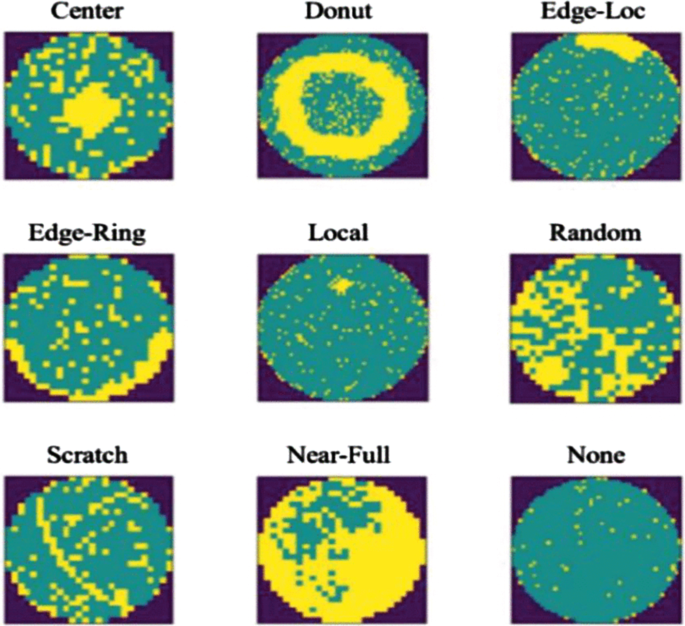
Nine wafer defects in dataset [1].
Conventionally, the defect detection is through visual examination of the wafers using a scanning electron microscope by a quality engineer. This manual method leads to a lot misinterpretation and is costly in terms of labour expenditures. Because the massive amount of data created in semiconductor manufacturing renders manual inspection exceedingly tedious and laborious hence improved methods are required. Wafer map pattern classification has seen significant progress, but conventional methods, lacking reliance on large-scale datasets, often fall short in accuracy. Researchers are increasingly turning to machine learning, particularly convolutional neural networks (CNNs), for wafer defect classification. The adoption of CNNs has notably improved classification accuracy. Additionally, researchers are addressing data balancing issues within the wafer map classification framework. This shift to deep learning-based methods, especially utilizing CNNs, marks a substantial improvement in accuracy and efficiency for wafer map defect classification.
Efficient deep learning architectures have indeed become a significant area of research and development, especially to address the challenges associated with high power consumption and large memory requirements in traditional deep learning models. Meeting the demand for effective deep learning architectures, which can achieve optimal performance while minimizing resource utilization, is imperative for the widespread adoption of AI applications. This is particularly crucial for devices with constrained computational capabilities. The ongoing research and development in the field are aimed at creating solutions that strike a balance between accuracy and efficiency, enabling the integration of deep learning into a broader range of devices and applications.
In this paper we propose a model that leverages multiplierless convolution with a CORDIC design and a systolic ring architecture-based dataflow to achieve efficient and high-performance deep learning computations. The method is in line with the broader goal of making deep learning models more accessible and practical for resource-constrained devices.
Several methods are there in literature for automatic defect detection in wafers. Based on whether the class labels of wafer maps are known in beforehand, the task of wafer map categorization can be split into two types: supervised learning and feature extraction. In a supervised learning approach, support vector machine (SVM), neural network, alternating decision tree, CNN, Fisher discriminant classification, general and simple sub spaced regression network, and ensemble-based method are widely used for WM classification [4].
Logistic regression and Support Vector Machines (SVM) stand out as the most commonly employed classifiers in Machine Learning (ML). Given the multitude of approaches available, identifying a reliable method is crucial for evaluating classifier performance. In the realm of semiconductor wafer fault pattern classification, Chen et al. [5] employed an adaptive resonance theory network called ART1, a neural network with binary input values and an unsupervised nature. A vigilance test is utilized for pattern learning. Other researchers have explored the use of Dynamic Time Warping in conjunction with diverse classifiers such as kNN [6] and SVM [7] to enhance classification accuracy. Ruifang et al. [8] achieved notable success by employing ZF-Net to extract features from dark field illuminated images, reporting up to 11 defect markers. They also harnessed powerful GPUs for increased computing performance. Several researchers have integrated Dynamic Time Warping with various classifiers, including kNN and SVM, to improve classification. Saqlain et al. [9] proposed WMDPI, an ensemble-based classification model that combines different ML classifiers. However, it necessitated substantial manual inspections.
From most of the previous works, it can be concluded that almost many of the classifiers require labour for extracting features and for that experienced semiconductor engineers are required and it will be a complex process. Therefore, such models can be expensive and tedious in the case of huge datasets. Here comes the advantage of classifying methods based on deep learning (DL). CNNs are the best example for that, it do not need manual extraction of features. CNNs demonstrate exceptional efficacy in deep learning methodologies, particularly when applied to the identification of defects in images. Some of the works are Nakazawa et al. [3] applied CNN for the classification of 22 WM defects. Because of data imbalance only some data was used to train and validate the model. Single and mixed defect patterns on same WM was classified by Kyeong and Kim [10]. B. Devika et al. [11] introduced a CNN model designed for detecting both single and mixed defect patterns. A CNN model proposed by Cheon et al. [12] can classify five different defect patterns by extracting features from the real wafer image. By fusing it with k-nearest neighbours (k-NN) unknown defect classes were also identified. The models can achieve high training accuracy if we are using bigger datasets. Imbalanced distribution of classes may cause bias of the model to the class with majority data. Muhammad Saqlain et al. [1] has done data augmentation and thus balanced the dataset and proposed a deep CNN model which can classify 9 defect classes and it achieves an accuracy of 96.2%. Here we propose a method using CNN for classification of nine defects in the wafer.
While considering the hardware implementation, most of the earlier works on CNN hardware implementation has mostly given priority to the data reuse and quantization scheme. There were many low latency methods which adds for hardware of the systems. Some works go for multiplierless methods but accuracy became a constrain there. But in [13] an efficient multiplierless method had been proposed based on [14] which provides a better result specially in terms of power consumption, which had been tried out here.
Methodology
The methodology of CNN for wafer defect detection mainly consists of collection of datasets, data pre-processing, augmentation of dataset and CNN model as shown in Fig. 2.

Block schematic of the proposed method.
The dataset used here is WM-811K. It is a large dataset which is available publicly in MIR laboratory website. The dataset consists of 811,457 real WM images that were taken from 46,293 lots in a circuit probe (CP) test. Even though each lot should contain 25 WMs, some of them were blank because of failure of sensor and some other reasons which were not known. In the dataset, majority wafers are having no-label, 18.2% wafers are marked as none category and 3.1% wafers with failure patterns. Figure 3 depicts the visualization.

Visualization of dataset distribution.
From the 21.3% of wafers experts were able to detect 9 types of defect failure pattern such as Center, Donut, Edge-Loc, Edge-Ring, Loc, Random, Scratch, Near-full, none. Figure 3 has the defects type. Among this 1,47,431 were None defect that is about 85% of the available wafers and hence comes the problem of data imbalance. The dataset also contain other information like die size, lot name, wafer index and train/test labels.
Highly imbalanced data adds to the challenge because most learners will be inclined toward the majority class and, in severe situations, may disregard the minority class entirely. Class imbalance will lead to over training of the CNN model. Class imbalance means some classes in dataset will contain large data while other classes may have less data. It is very necessary to resolve this issue and this is done by data augmentation technique. Data augmentation refers to the method of enhancing the volume of data by incorporating slightly modified duplicates of existing data or generating synthetic data based on the existing dataset. Some of the data augmentation techniques are shifting, flipping, zooming and rotating. Image shifting involves displacing all pixels within the image in a specific direction, either vertically or horizontally, while maintaining the image dimensions. Flipping, on the other hand, entails reversing the order of pixels in either rows or columns, corresponding to vertical or horizontal flips, while preserving the image’s size. Rotation augmentation introduces a random clockwise rotation of the image by a specified degree, ranging from 0 to 360. Zoom augmentation randomly adjusts the image scale, either by adding new pixel values around the image or through pixel value interpolation. Here we have done horizontal and vertical flipping and the number of images increased to about 270000 with all class having almost same number of images. 30% of the data taken for testing and remaining for training. Another problem with the dataset was different sizes of wafer images, so all of them were resized as (50–50).
Proposed CNN model
From the previous work studies, we can understand that there are many works related to classification of the semiconductor wafer defects. Here we have proposed a simple CNN model with less number of layers thus reducing complexity and it also achieved good accuracy. The model consists of 3 convolutional layers, 2 max pooling, 1 global average pooling and 3 fully connected layers. The proposed CNN architecture is shown in Fig. 4.

Proposed CNN model.
The input image given to first convolutional layer is (50×50) images and it has 10 filters of size (3×3) to extract features from it. By the increment of the depth of the convolutional layers the filters given will also be increased. This will increase the feature maps. But the pool layer will decrease feature maps. ReLU activation function is added on almost all layers other than max pooling layers. This is to eliminate the Vanishing Gradient Problem (VGP). It is a circumstance where a recurrent neural network or a deep multilayer feed-forward neural network is unable to transmit valuable gradient information from the model’s output to the layers close to its input. As a result, models with several layers are generally unable to learn from a given datasets or prematurely converge to an inadequate solution. Numerous solutions and workarounds, including alternative weight initialization techniques, layer-wise training, unsupervised pre-training, and variants on gradient descent, have been suggested and researched. The usage of the rectified linear activation function, may be the most prevalent shift. It will keep all the positive values without any change and the negative values get swapped with zero. The pooling layers will downsample the data and the kernel size here is (2×2).
Here global average pooling layer is used. Usually flatten layers are used to obtain 1D tensor. as an alternative to the flatten layer, which is added after the last pooling block of our CNN. Global Average Pooling conducts average pooling over spatial dimensions, reducing them to one, while keeping other dimensions unaltered. A key advantage is the prevention of overfitting at this layer since it has no parameters. Additionally, global average pooling incorporates spatial information, making it robust to spatial translations in the input. The results from the global average pooling layers are then fed into fully connected layers for the initiation of classification. Subsequently, the SoftMax activation function is applied at the output. Softmax is chosen when dealing with more than two classes, as in this case where there are nine classes.
The optimization algorithm employed in this context is Adam optimization. Optimizers play a crucial role in adjusting a neural network’s parameters, such as weights and learning rates, to minimize losses. Adam serves as a substitute optimization algorithm for stochastic gradient descent in the training of deep learning models. It amalgamates the favorable characteristics of the AdaGrad and root mean squared prop (RMSProp) algorithms, making it well-suited for handling sparse gradients in noisy problem domains. Adam is known for its relative ease of configuration, with default parameters often proving effective across a variety of problems.The loss function applied here is categorical cross entropy.
An approach for multiplierless convolution in a hardware-friendly manner, avoiding the use of dedicated multipliers is presented in this section. Relying on adders and low-width shifters can significantly reduce the hardware complexity and resource requirements, making it well-suited for convolution implementation in CNN.
The Coordinate Rotation Digital Computer (CORDIC) algorithm is an efficient method, especially in scenarios where avoidance of dedicated multipliers is a priority. It can be used to calculate trigonometric values. Consider a vector M with coordinates (l,k), trigonometric functions like sine and cosine, can be obtained by rotating through an angle ∅ then a new vector M′ is obtained. This rotation method is used [13] to eliminate the use of multipliers.
Modified convolution
In [13], the first approach for calculation of output feature maps is demonstrated by
Scaling down of weight by 2-α[p] (where α[p]∈N is a scaling coefficient) will preserve the features generated by convolutional layers [13]
The weight value W [p] [k] [x] [y] 2-α[p] can be replaced by trigonometric function in range [-1, +1]. The CORDIC convolution operation can be [13]
Suppose we are considering the convolution between a 3 × 3 input and 3 × 3 weight values, requiring 9 processing elements (PE). Each product term in Equation (3) is computed by a respective PE unit. The input to the modified PE [13] (Fig. 5) consists of pixel data (in), a direction sequence (b), and the output of the preceding PE. Both in and b are 8 bits. The selection line b [7] is introduced at the input. A tan -12-1 rotation is performed if the value of b [6] is 1′ b1, and a rotation of 90° is executed if b [6] is 1′ b1. The remaining values of b correspond to micro-rotations, as in [14]. Therefore, for each PE unit, 3 cycles are required, resulting in a total of 27 cycles for the 9 PE unit. A processing element using CORDIC is shown in Fig. 5.

CORDIC based processing element.
The model was created by using libraries TensorFlow and Keras in Google Colab. The number of epochs were 50 and batch size was 32. The experiment was conducted on personal computer with following specifications: Intel(R) Core(TM) i3-1005G1 CPU @ 1.20GHz, 4.00 GB RAM and x64-based processor. The CORDIC PE unit was done on Xilinx ISE 14.7 and the device was Spartan 6. A normal convolution is also done in the same platform for comparing the power efficiency.
Performance of CNN model for wafer defect classification
Class wise recall, precision and F1-score
Class wise recall, precision and F1-score
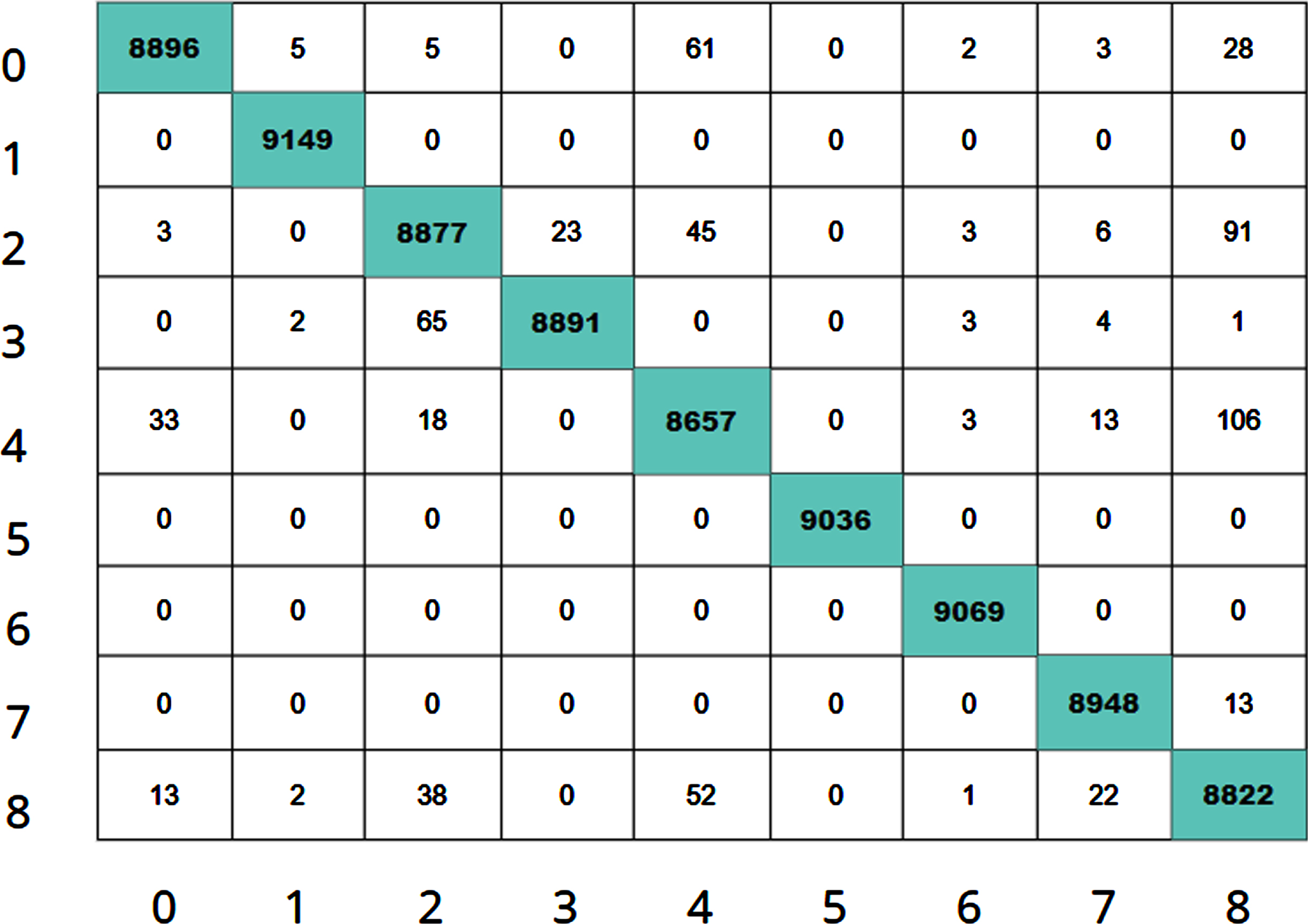
For analyzing the model different performance measures like accuracy, precision, recall, and F1-score are used. The accuracy of the model is obtained as 99.1%. From Table 1, recall, precision and F1-score of each class can be obtained and in the table 0, 1, 2, 3, 4, 5, 6, 7, 8 represent Center, Donut, Edge-Loc, Edge-Ring, Loc, Near-full, None, Random and Scratch respectively.
The confusion matrix, of the model is shown Fig. 6, from which the mislabelling of the classes can be identified and it is comparatively less.
Confusion matrix.
The Fig. 7 shows the performance comparison of the proposed model with previous works. From table it is clear that all the performance metric of the proposed model has a upper hand than others.

Performance comparison.
Multipliers are the most power and area consuming component in a circuit. It is very necessary to reduce or eliminate the number of multipliers. We had done CORDIC based PE and conventional PE unit and it is observed that there is much reduction in power when using CORDIC based PE unit, because of the elimination of multiplier units. For normal convolution it was obtained 322 mW and for CORDIC based it is 17 mW.
Conclusion
Here a deep learning-based CNN model is proposed to classify wafer map defects in the semiconductor fabrication process. The model is less complex by having only nine layers and demonstrates good performance with an accuracy of 99.1%. The result was realized using dataset WM-811K consisting of nine wafer defects. For the hardware implementation of CNN, a model using multiplierless convolution is realized in FPGA using CORDIC which has less computational power and proved efficient than coventional ones.