
Abstract
In this work, we investigated the effect of the thickness on structural, morphological, optical, and electrical properties of In2O3 thin films synthesized via by sol–gel spin coating technique. The prepared samples were characterized by various techniques including X-ray diffraction (XRD), scanning electron microscope (SEM), energy-dispersive X-ray (EDX) spectra, UV-Vis-NIR spectrophotometer as well as the electrical measurements via the four-probe technique. The XRD analysis reveals that the films have a cubic crystalline structure, with (222) preferential orientation. The crystallite size values of the films were varied from 14 to 27 nm. The (SEM) images indicated that the homogenous and smooth surface with better adherent to the substrate surface. The EDX spectrum reveals the presence of In and O element necessary for In2O3 films for film formation. Excess of oxygen is observed due to the substrate contribution. The transmittance results exhibit that the films are highly transparent, more than 75% in the visible range from 400 nm to 800 nm is measured. The estimated band gap energy is found to increase with increasing film thickness (3.37–3.7 eV). The electrical resistivity of the In2O3 thin films substantially decreases with the increasing film thickness from 1.48×10⁻⁴ to 1.3×10⁻³ Ω.cm.
Introduction
In the last few years, human existence is becoming semiconducting thin films dependant. The latter play important role in all fields especially field of optoelectronic, microelectronic and communication technologies [1]. Among them, the transparent conductive oxides (TCO) such as SnO2, CdO, ZnO, In2O3, TiO2 etc [2–4] have been extensively studied, because of their unique physical and chemical properties, they found a large number of applications, such as photovoltaic solar cells [5], sensor devices [6], light-emitting diode devices [7] and flat panel displays [8]. Among these oxides, In2O3 is an important one, it is well known as a suitable material for many electronic applications due to its excellent physical properties. It is an n-type semiconductor with a wide band gap (Eg ∼ 3.65 eV) [9], a high refractive index (2–2.1) [10] as well, high optical transmittance (in the visible region) and good electrical conductivity [11]. Thus these properties allow for photovoltaic devices, solar cell, transparent windows, liquid crystal displays, light emitting diode (LED) and gas sensors to be realized [12–14].
Several researchers have studied the effect of several parameters on the structural, optical and electrical properties of Indium (III) oxide (In2O3) in order to improve their properties [15–20], using different method. The films thickness is one of the most important decisive factors for film physical properties. The lack of thin In2O3 film thickness in the literature motivated us to study the influence film thickness on physical properties of In2O3 films. Few published papers emphasized that the film thickness has a significant effect on the physical properties of In2O3 film [21, 22]. However, only a few studies have been devoted to the influence of large film thickness (d > 800 nm) on the physical properties of In2O3 films deposited by sol gel spin coating process.
By the way, several deposition techniques have been widely used to produce In2O3 thin films including RF magnetron sputtering [23], chemical vapor deposition (CVD) [24], spray ultrasonic [25], thermal evaporation [26], spray pyrolysis [27], pulsed laser deposition (PLD) [28] and sol-gel methods [29]. Among these, sol–gel method is one of the most used techniques for In2O3 thin films preparation compared to others deposition methods, due to its significant advantages such as simple, economical relatively cost-effective process. It allows the easy and precise control of material composition and films production with a good quality [30–32].
This paper reports the effect of film thickness on structural, morphological, optical and electrical properties of In2O3 thin films prepared by sol–gel spin coating process.
Experimental details
Materials and In2O3 thin film preparation
The undoped indium oxide (In2O3) thin films have been grown by sol-gel spin coating technique. Indium (III) nitrate hydrate (In(NO3)3·H2O), 99.98% pure (Sigma–Aldrich) (0.43 g), that was used as source material of In+3 and it was dissolved in appropriate amount of ethanol (C2H6O) (9 ml) and acetylacetone (C5H8O2) (1 ml) as the stabilizer, with 0.15 M concentration. The volume ratio of acetyl-acetone to ethanol was maintained at 1:10. The starting solution was stirred for 2 h at 50° C, then mixed and stirred with a magnetic stirrer for 24 h at room temperature to obtain a transparent solution. Soda lime glass (SLM) slides were used as substrates with the size of (2.5 cm×2.5 cm×0.15 cm). Before the deposition, the glass substrate was cleaned followed by rinsing in methanol and acetone for 10 min then cleaned with deionized water for 5 min and dried in air.
The prepared solution was dropped onto cleaned glass substrate, with rotation speed of 4000 rpm for 30 s in order to obtain a well coated thin film on glass substrates. Subsequently, the coated films were dried at 250° C for 10 min after each successive coating in a furnace to evaporate the organic solvent. The procedures was repeated 4, 6, 8, 10 and 15 times (number of layers) in order to achieve various In2O3 thin film thicknesses. Finally, the film was annealed at 550° C in the furnace for 1 h. A schematic drawn representing the In2O3 thin film preparation steps are sketched in Fig. 1.
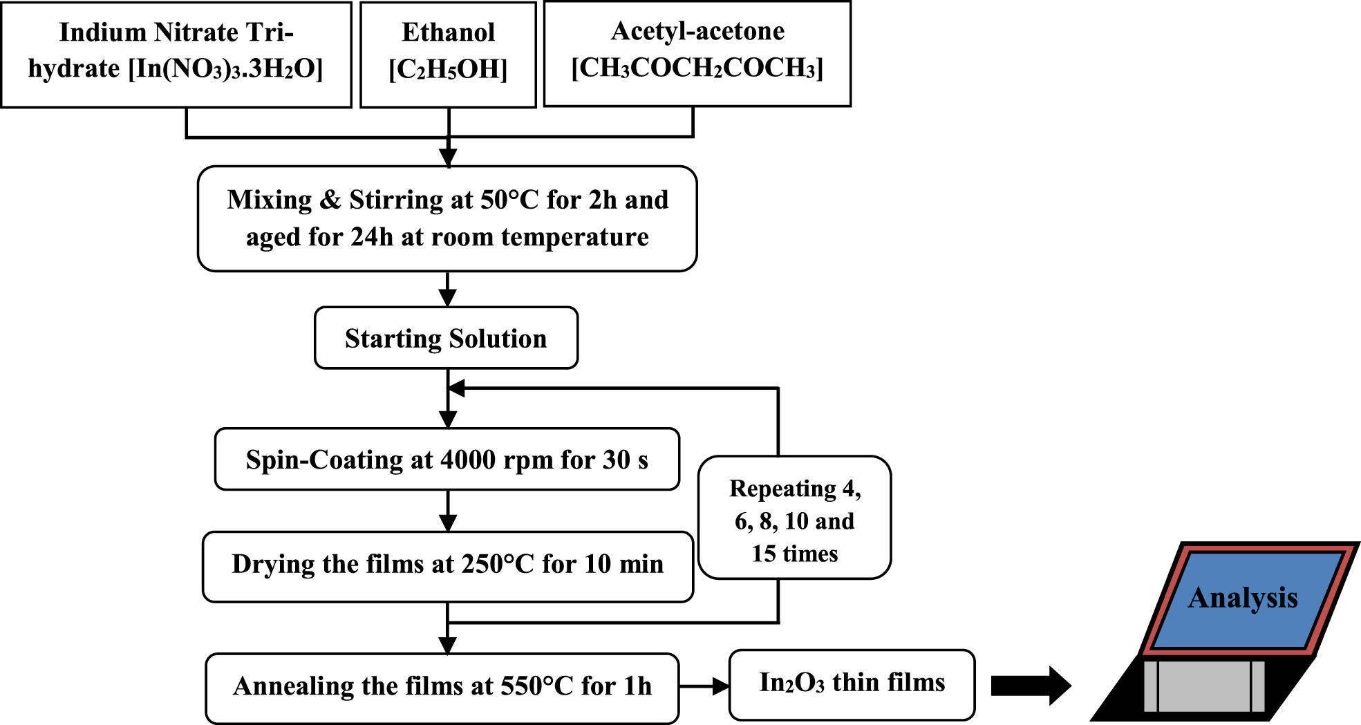
Flow chart showing the schematic diagram for In2O3 thin film preparation procedure.
The structural, morphological, optical and electrical characterizations of all the films were treated by using various techniques. The crystallinity of the samples was characterized by X-ray diffraction (Model: Bruker D8) using Cu Kα (λ= 1.5418 Å) radiation within the 2θ range of 10°–90°. Moreover, observation of surface morphology was achieved using a scanning electron microscope (SEM JEOL model VEGAS3 TESCAN). The films composition was analyzed by energy dispersive analysis using X-rays (EDAX) equipped in “VEGAS3 TESCAN”. The optical transmittance was recorded using UV-Visible spectrophotometer (Perkin Elmer Lambda 950 UV/VIS) in the wavelength range 200 to 1000 nm. Finally, the measurements of electrical resistivity were carried out by a four-point configuration, using “Jandel RM 3000” apparatus at room temperature. Carrier concentration and mobility were measured by Hall effect measurements system using gold contact electrodes with applying the magnetic field 0.6 T and current 3 mA.
Results and discussion
Structural properties
To films thicknesses of In2O3 thin film was controlled by varying the number of the layers from 4 to 15 layers. The film thickness was determined using SEM cross sections by calculating the average thickness from one end to the other as depicted in Fig. 2. As shown in Fig. 3, the thickness of the films increases with the number of the layers, the variations follow a quasi linear behavior with a rate of 58 nm per cycle. Form the linearity depence one can choose the number of cycle suitable to obtain a desired thickness.
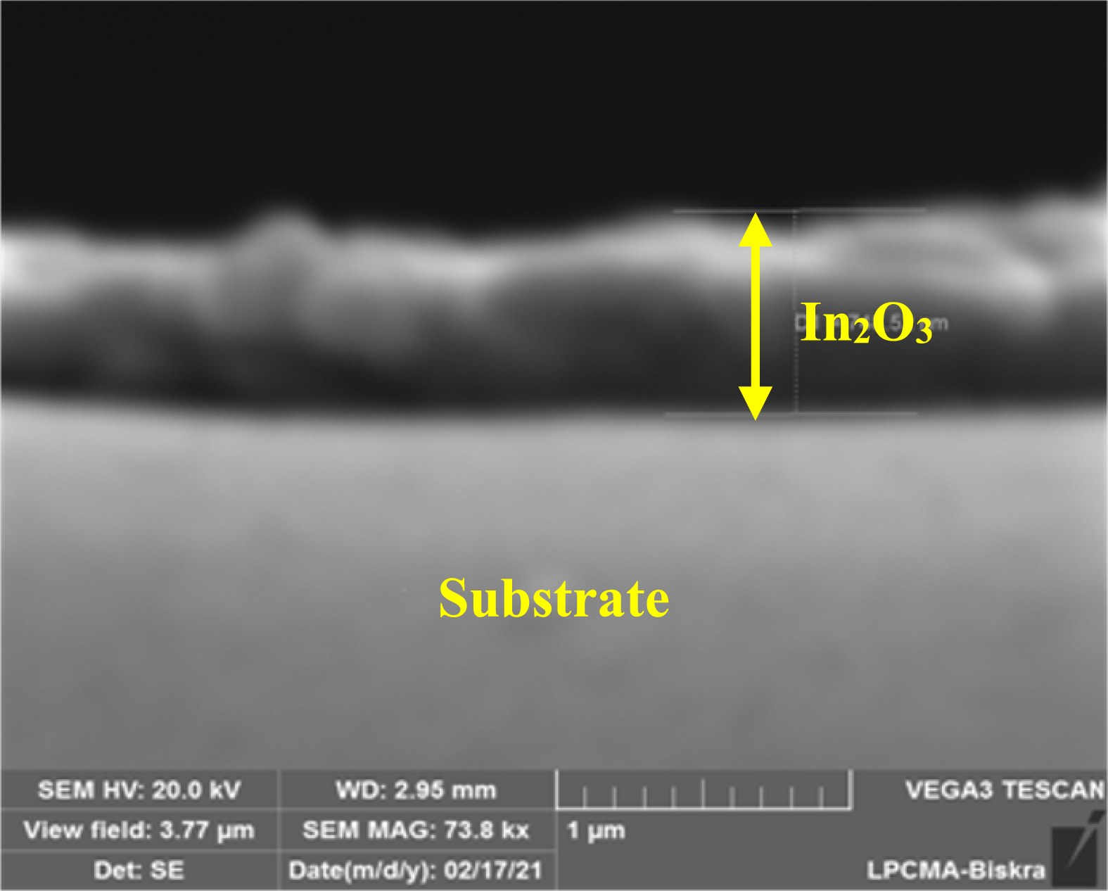
Direct thickness measurement of the film of In2O3 from the cross sectional SEM images.
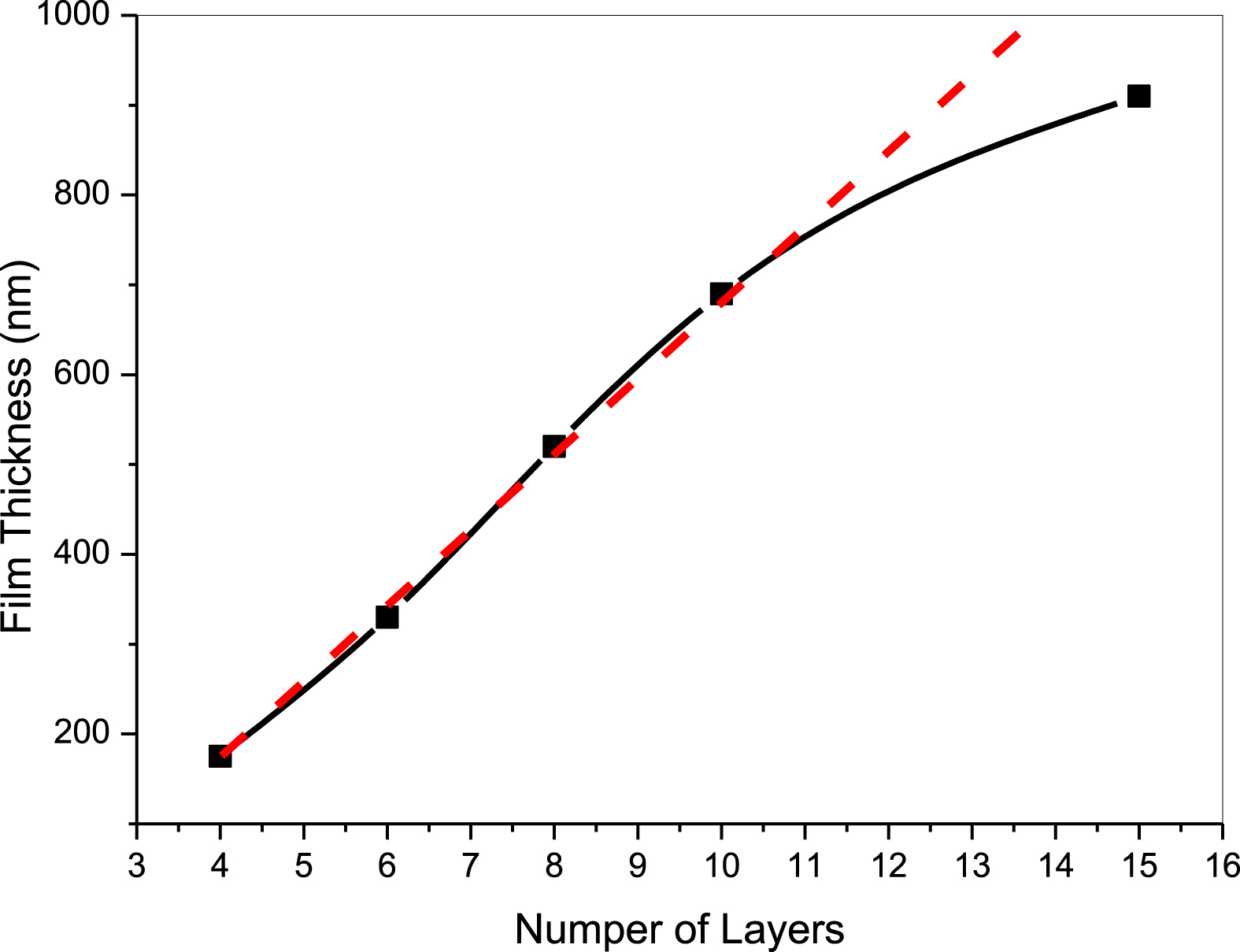
Variation of the film Thickness with the number of layers.
The crystal structure and orientation of the In2O3 thin film were investigated by X-ray diffraction (XRD) pattern. The XRD pattern of all In2O3 films prepared at different film thickness (175, 330, 520, 690 and 910 nm) on glass substrate are shown in Fig. 4. As can be observed in the graphic, the samples have a polycrystalline structures with five peaks shown in Fig. 4, assigned to (211), (222), (400), (440) and (622) diffraction planes, matching with a body cantered cubic (BCC) phase of In2O3 with a space group of Ia3(206) (JCPDS Card No. 06-0416, space group, a = 10.118 Å) [33]. However, no peak related to a secondary phases such as In or InO is observed. Similar result has been observed in our earlier work and other work [34, 35]. Moreover, Fig. 4 reveals that the samples have an intense peak originating from the (222) diffraction plane, it becomes narrower, intense when the film thickness increases, suggesting the films crystallinity improvement. The preferential growth along (222) direction may be due to the reasons that the plan (222) requires the lowest free surface energy formation [36, 37]. The data also shows that the peak position slightly shifts to a lower 2θ value as shown in Fig. 5, this is probably due to stress created during the films growth.
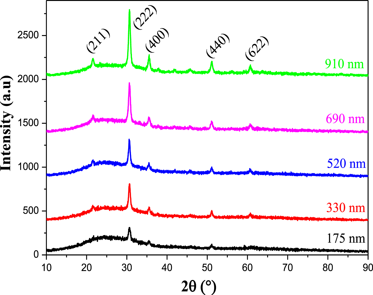
XRD patterns of nano-crystalline In2O3 thin films for different film thickness.
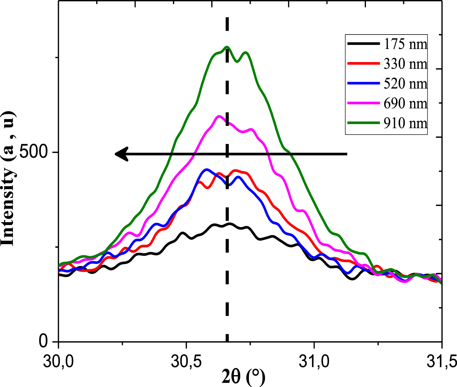
Variation of peak (222) position of In2O3 thin films at different film thickness.
To describe the preferred growth orientation (h k l), we calculated the texture coefficient from the X-ray data using the following equation [38]:
Where I (h k l) is the measured intensities of the plane, I0(h k l) is intensities of the standard plane (h k l) (JCPDS data card (6–416)) and N is the number of diffraction peaks. The obtained results summarized in the Fig. 6. It is clear that the (222) direction has the highest texture coefficient comparing with other peaks, which increases drastically with increasing film thickness. It is well known that the films texturation is usually related to two factors: the growth and nucleation. The increase in the preferred orientation of (222) plane is attributed to the increasing in the growth along this direction on the detriment other planes.
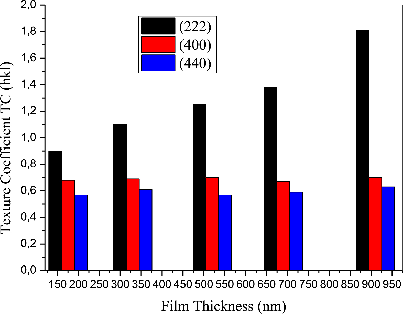
The texture coefficient of In2O3 thin films as function of film thickness along (222), (400) and (440) directions.
The crystallite size (D) was estimated from the FWHM of the high intense peaks, namely the one corresponding to (222) crystallographic plane, using the Debye–Scherrer formula [39]:
Where λ is the wavelength of the X-ray (λ= 1.5418 Å), β is the full width half maximum of the diffraction peak expressed in radians and θ is the Bragg diffraction angle.
The dislocation density (δ) and strain (ɛ) were calculated using the following equations [40, 41]:
The calculated crystallite sizes, strain and dislocation density is listed in Table 1.
Crystallite sizes, dislocation density and strain values of In2O3 thin films extracted from XRD analysis
It is evident from the contents of Table 1 and Fig. 7, that as the films thickness increases, the crystallite size enlarges, while the strain decreases. The same behavior is reported by Goswami et al. in his study on In2O3 thin films prepared by pulsed laser deposition technique [42]. On opposite, in our previous work [43] we have noticed a decrease in crystallite size with molar concentration increase. The observed improvement in crystallite sizes is commonly attributed to sufficient supply of thermal energy to the coalescence the atoms over the surface substrate and this facilitate the merging of the smaller particles into larger ones, as the results, the crystallite sizes increases [44, 45]. The decrease in strain formed in the crystal could be related to improvement of the crystallinity, which result to produced more organised films with less point defects.
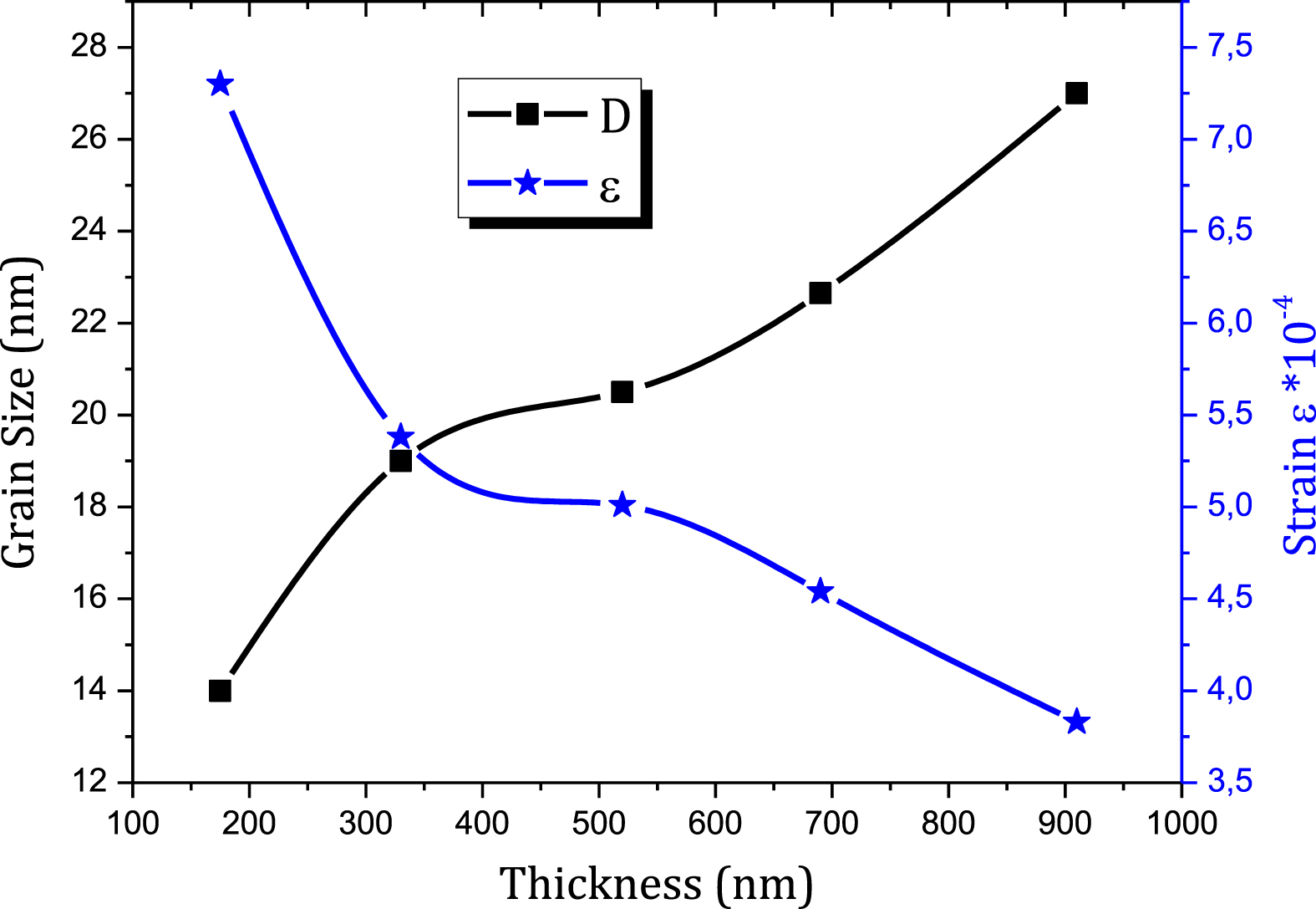
The evolution of grain size and strain of In2O3 thin films at different film thickness.
The inter-planar distances d
hkl
and the lattice constant a for a body-centered cubic structure of In2O3 films were estimated according to Bragg’s law as Equation [46]:
Where θ hk is the diffraction angle and λ is the X-ray wavelength (1.5418 Å) and hkl is the Miller indices.
In order to calculate the deformation in the lattice parameters of bulk, the internal stress needs to be determined. For cubic crystals, the internal stress (σ) in the plane of the film can be estimated using the following equation:
Where a is the lattice constant measured from the XRD, a0 is that of bulk lattice constant (10.118 Å), E is Young’s modulus of In2O3 (145 GPa) [47], γ is the Poisson’s ratio (0.31) for In2O3 [48].
The calculated structural parameters from XRD pattern of In2O3 films are summarized in Table 2. As can be seen from Table 2 the a lattice parameter of pure In2O3 thin films increases with the films thickness. At the same time, the internal stress changes from compressive (negative) to tensile (positive). The similar result observed in previous study [49, 50]. It can be seen that the compressive stress in the films decreases and in contrary, the tensile stress increases with increasing films thickness.
Structural parameters information of prepared In2O3thin films for different films thickness
The surface morphology images of as grown In2O3 thin film having different thickness is presented in Fig. 8 (a)-(e). It can be seen that all the films have a uniform, smooth, continuous and homogenous surface morphology with particle distribution consisting of spherical and triangular shapes without any voids and cracks. However, with the increases of film thickness, a large number of granular and dense grains are formed on top of the film. As can be seen, the grain size increases with increasing of film thickness. This result is supported by obtained results in the XRD analysis.
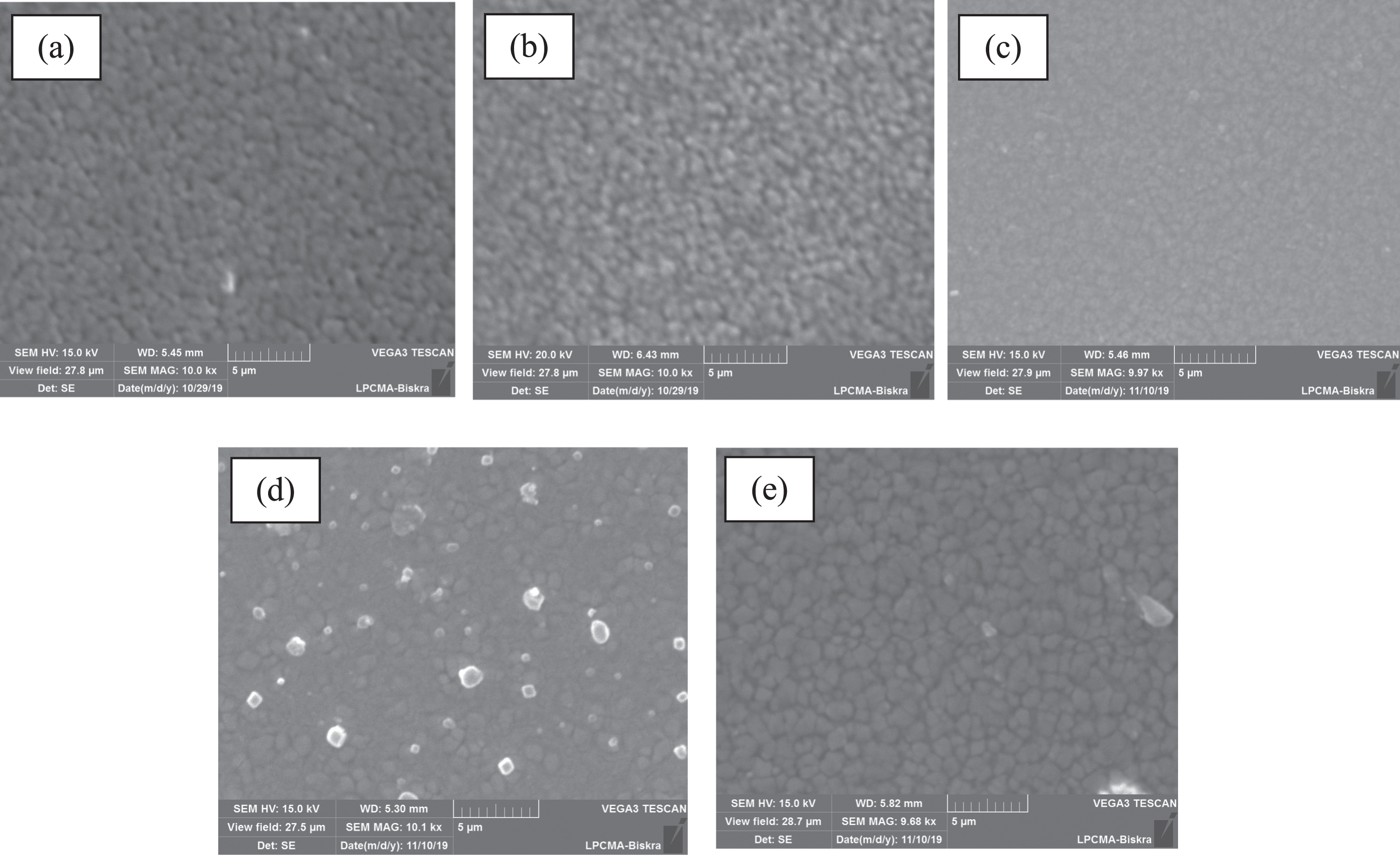
SEM micrographs of the In2O3 thin films at different film thickness: (a) 175 nm, (b) 330 nm, (c) 520 nm, (d) 690 nm and (e) 910 nm.
The EDX spectra of In2O3 thin film deposited with different films thicknessare reported in Fig. 9. The EDX study confirms the presence of indium (In) and oxygen (O) necessary for In2O3 formation. The silicon originates from the glass substrate. In a stoichiometric In2O3 the atomic percentage shoud be 60% and 40% for Oxygen and Indium, respectively. However, according to the EDX spectra (Fig. 9) the films contain an excess of oxygen, this might be due to the contribution of oxygen originating from the substrate as well as Si atoms. On the other hand the excess of oxygen may also originate from the existence of oxygen vacancies [51].
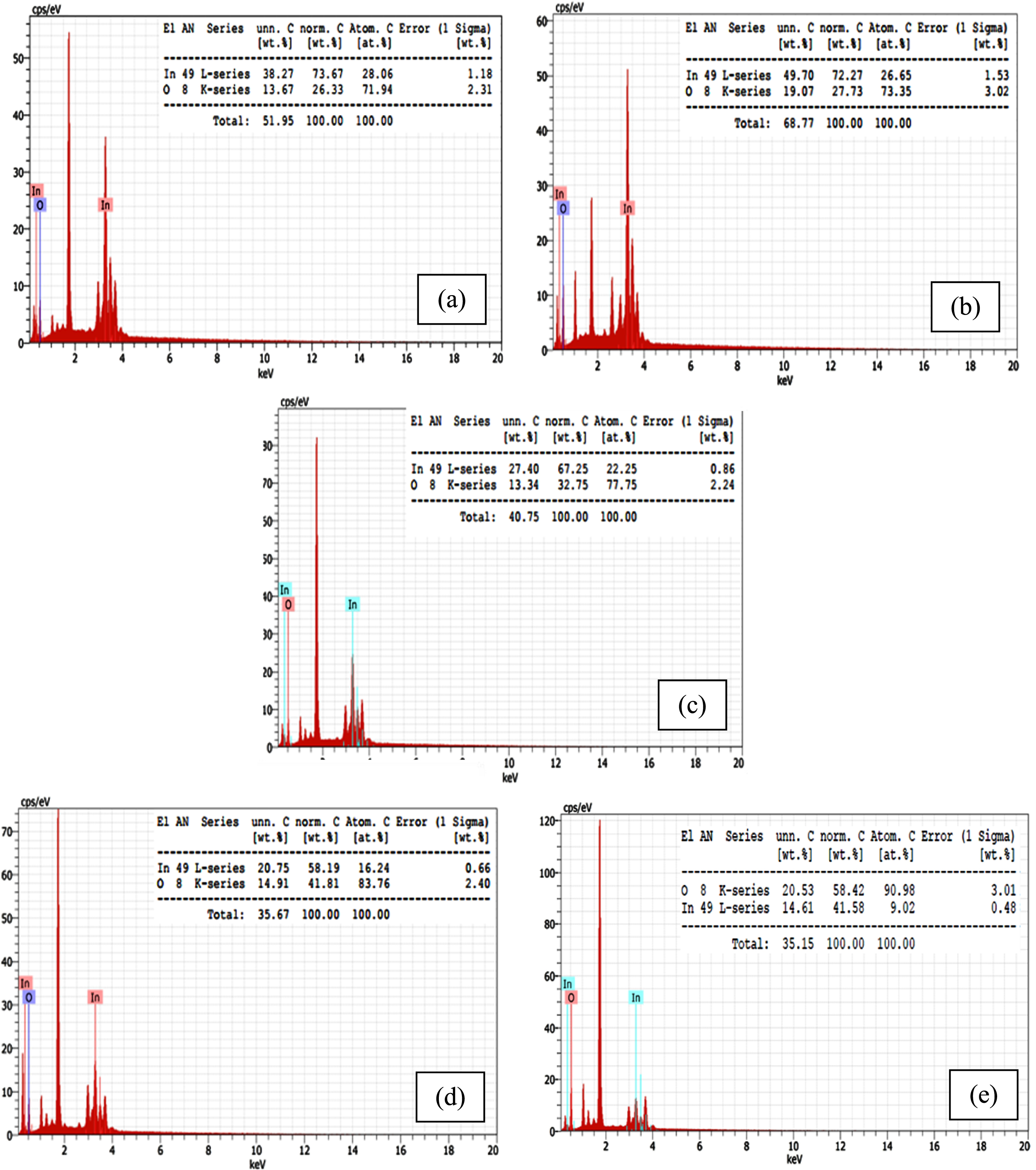
EDX spectrum of the In2O3 thin films at different film thickness: (a) 175 nm, (b) 330 nm, (c) 520 nm, (d) 690 nm and (e) 910 nm.
The transmittance spectra of the indium oxide thin films in the wavelength range of 200–1000 nm are shown in Fig. 10. All of the samples exhibit high optical transmittance more than 75% in the visible wavelength region (400 to 800 nm). The high transmittance of these films can be appropriated as transparent electrode of the solar cell application [52]. Interference fringes are noticeable in the visible region, this indicatives of uniform and homogenous obtained films which are characteristically smooth [53, 54]. Hence, the reduction in the light scattering losses due to the films smoothness is the principal reason of the films transmittance improvement. Besides, the transmittance spectra of our samples revealed strong absorption edges in the UV region (λ< 380 nm), which suggesting the blue-shifted absorption edge with the increasing films thickness, as shown in the inset of Fig. 10. This phenomenon has been reported in other TCO thin films [55, 56].
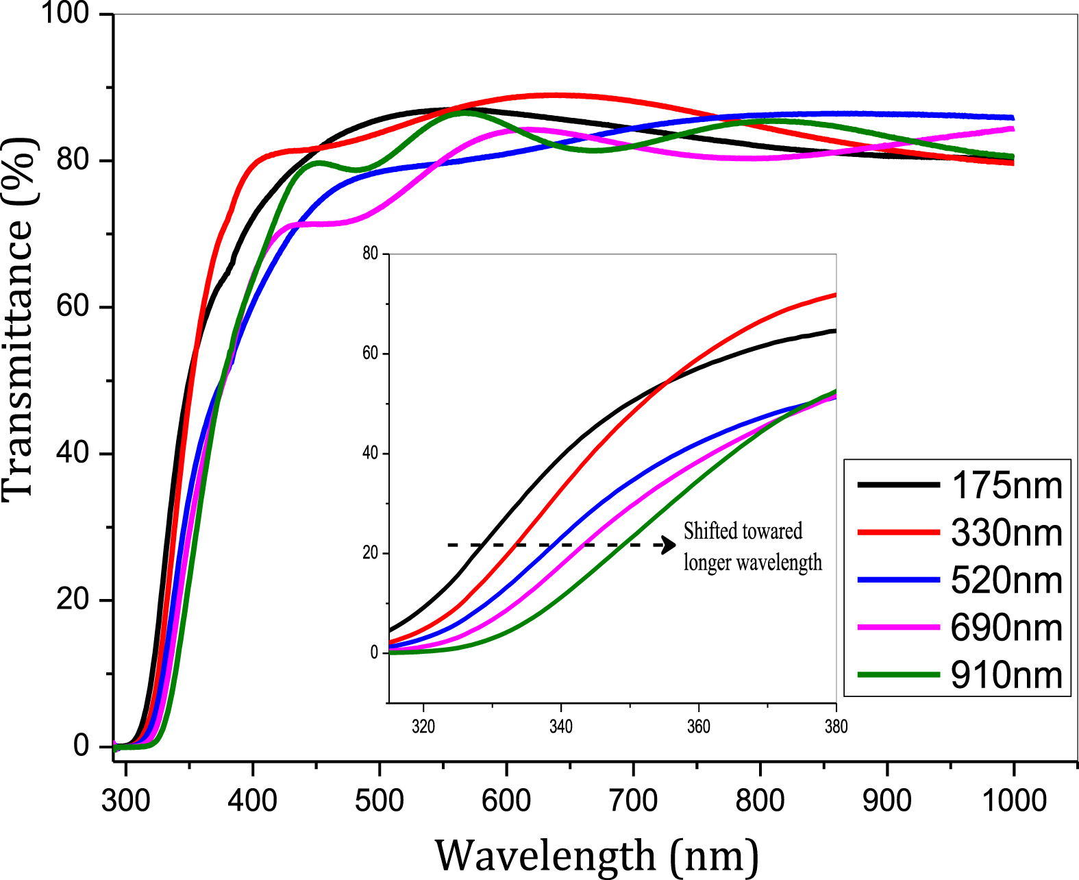
The transmittance spectra of In2O3 thin films prepared with various film thickness.
From the curve of (αhν)2 as function (hν) which depicted in Fig. 11, the optical band gap (Eg) can be determined by the extrapolation of the linear region of the curves to intersect at hν axis following Tauc relationship [57]:
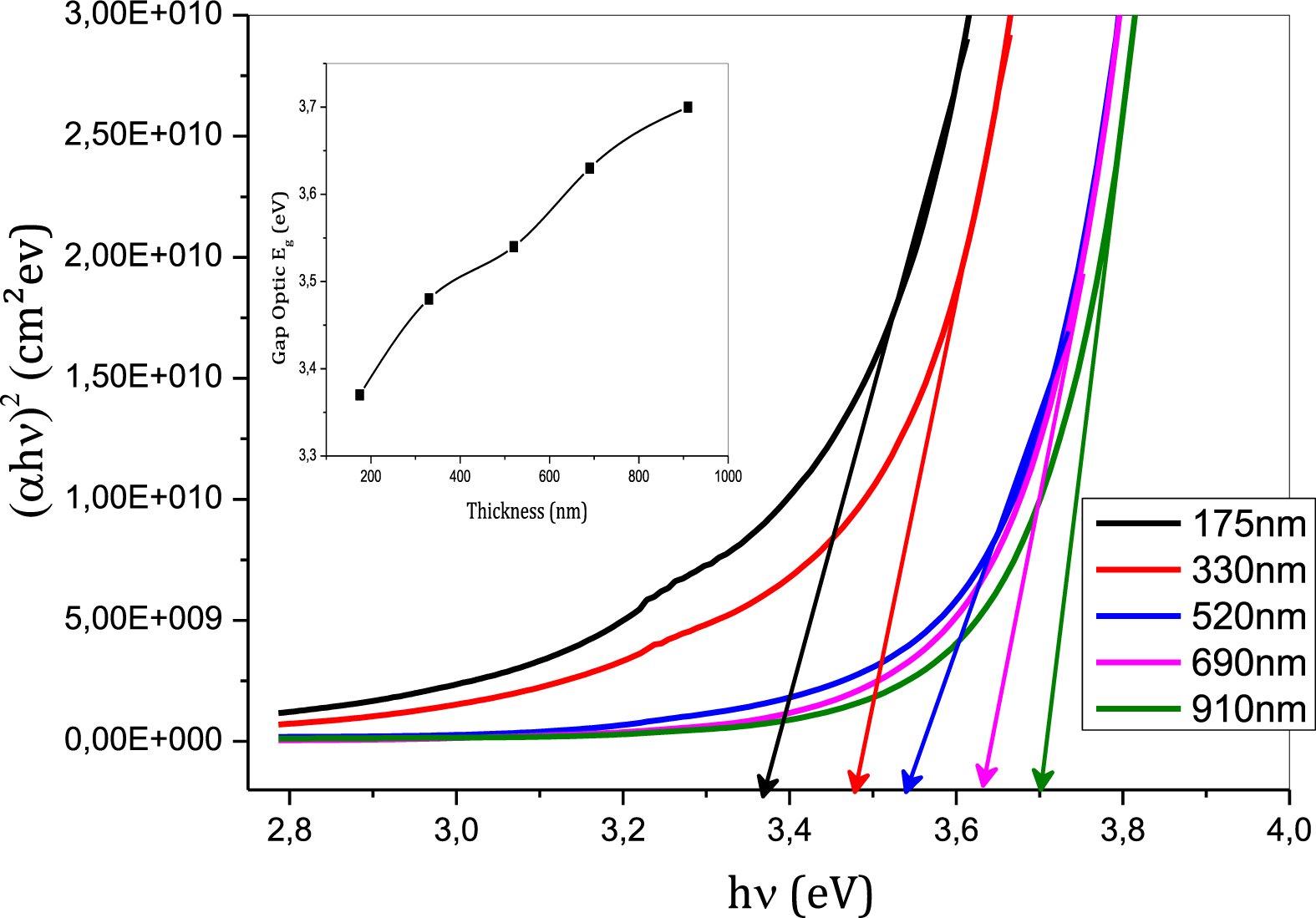
The plot of (αhν) 2 against hν of In 2O3 thin films and inset shows the variation of optical band gap (Eg) as a function of film thickness.
Where A is a constant, hν is the photon energy, E
g
is the optical band gap energy and α is the absorption coefficient, which calculated as [58]:
Where d is the thickness of the sample.
The inset image as shown in Fig. 11, represents the calculated band gap values dependence on the films. The observed band gap values are in good agreement with the reported value for the ITO films deposited by electron beam evaporated and RF sputtering technique [59, 60]. The broadening of band gap energy with the increasing films thickness can be due to the Burstein–Moss effect [61, 62]. This phenomenon is related to increased carrier concentration which lead to shifts the Fermi level to higher energy [63, 64].
FTIR spectroscopy was used to reveal the chemical bond present indium oxide (In2O3) thin films. Figure 12 represents the FTIR spectra of indium oxide (In2O3) thin films with various films thickness. A sharp absorption peak centered at 2354 cm–1 is attributed to the O–H stretching vibration from absorbing water molecules (H2O) in In2O3 lattice [65]. However, we can also recognize absorption band at 906 cm–1 related to C–H bending vibration. The weak intense bands around 766 cm–1 are ascribed to In–O lattice stretching vibrations [66], because the In–O stretching vibration modes are usually observed in the region of 800–300 cm–1 as reported by many authors [67, 68].

FTIR spectra for In2O3 thin films deposited as a function of film thickness.
Table 3 illustrates the variation in resistivity (ρ), carrier concentrations (n), and Hall mobility (μ) of In2O3 thin films as a function of films thickness. As shown in Table 2, the resistivity decreased from 1.5×10⁻³ Ω·cm at 175 nm to 1.5×10⁻⁴ Ω.cm at 910 nm. At the same time, both of the carrier concentration and mobility of the films rapidly increase from 1.24×1021 cm–3 to 6.43×1021 cm–3 and 0.65 cm²/V.S to 33.7 cm²/V.S with increasing thickness, respectively. Similar results were reported in previous literature [69–71]. The resistivity reduced can be attributed to the films crystallization improvement, which leads to the enlargement in crystallite sizes which consequently reduces the free electron scattering at grain boundaries [72] and then the carriers mobility enhancement. On other hand, the presence of oxygen vacancies and/or interstitial indium acts as charge donor centers in the system consistent with the observed increase of the charge carrier density and mobility [73, 74]. The free carriers enhancement with the thickness is in good agreement with the films band gap broadening as deduced from the optical characterization results.
Electrical resistivity, carrier concentration and carrier mobility values of In2O3 thin films deposited using sol-gel spin coating method
Electrical resistivity, carrier concentration and carrier mobility values of In2O3 thin films deposited using sol-gel spin coating method
In summary, high transparent conducting In2O3 was successfully prepared on glass substrates using a sol-gel spin coating technique. The structural, morphological, optical and electrical properties of In2O3 thin films have been investigated and analysis as a function of the thickness. The X-ray diffraction analysis indicated that the deposited thin films have a cubic polycrystalline structure with (222) as preferential growth direction. In addition, the crystallite sizes rises with the films thickness it increases from 14 to 27 nm. SEM images revealed that the prepared films are voids and cracks free and also the homogeneity and the smoothness of the films surface. The EDX spectra confirmed the presence of In and O elements. Furthermore, the prepared films have a good transmittance in the visible region above 75% with blue shift in band gap energy from 3.37 to 3.7 eV attributed to Burstein–Moss effect due to free carriers concentration enhancement with the films thickness increase. The FTIR spectroscopy measurements have have provided evidence of functional groups (In-O) proposed to be present in the chemical bonding. Electrical properties show that the films resistivity is reduced with increasing the film thickness. In conclusion we inferred that the film thickness is important parameter controlling In2O3 films physical properties.