
Abstract
This research paper discusses the performance enhancement techniques of multi-layered OLED structures. OLED’s electrical behaviour is evaluated using an analytical model using benchmarked industry-standard Atlas 2-D numerical device simulator. It highlights the extraction of emission and charge transport phenomena and charges injection role. Multilayer OLED device has been investigated by extracting the key performance parameters, including the current density and luminescent power as a function of anode voltage. There is an improvement of 15% in the current density. Furthermore, this work has proceeded with internal analysis and using a mathematical model, where the electric field, total current density, electron and hole concentration, and internal device parameters have been extracted to understand the performance of OLED devices better. Additionally, the internal physics and behaviour of the device have been studied in terms of Langevin recombination. Internal analysis is performed by making cutlines in a vertical fashion so that device physics and the process occurring in the internal part can be clearly understood. The OLED device behaviour analysis is performed using the industry standard state of art device simulation tool.
Keywords
Introduction
Over the past decade, organic electronics have been a better choice for researchers to study in accordance with silicon technology. Organic-based devices facilitate the lightweight, easy fabrication steps, very thin and easily affordable with low cost [1]. Organic materials are advantageous on the ground of organic transistors such as digital circuits and storage devices like memories with very high yields in terms of performance. Thus, it gives way to the evolution of devices such as Radio Frequency Identification (RFID) and Organic Light Emitting Diode (OLED) etc [2]. OLEDs are at the front of display technology these days research. They facilitate flexibility and affordable fabrication cost [3]. They can be fabricated on a large surface with a huge amount of colour it can emit with low power requirements [4]. This could be one reason that’s why industries like Apple and Samsung use these devices in the display application. The limitation of these devices is not confined. They exhibit good luminance properties emitting uniform colour [5]. Their applications are also seen in sensor Visual Light Communication (VLC), and OLED lamps.
In the current era, OLEDs are being used by reputed industries like Apple, Samsung, LG etc, for display applications on a large scale. Thus, researchers are on the way to enhancing the performance of OLED for better utilisation. Several strategies are employed to improve its performance, like the static nature in material design [6], the dynamic nature of block layers in architecture [7], and the use of alternative electrode materials. In this research paper, different materials have been used to analyse the performance of OLED based on structure to improve various parameters.
Various OLED internal analysis has been carried out for the multilayer OLED architecture. This paper has been segmented into 4 parts including the introductory part. In the second part, the methodology has been discussed, which explains the proposed architecture of OLED and Device analysis through TCAD simulation. Section third explains the result and discussions. The conclusion and future applications are described in part four at the end.
Device structure and simulation setup
This section describes the depth analysis of OLED and performance parameters extraction using the state-of-the-art Silvaco ATLAS simulation tool and with the help of conventional mathematical equations.
Device structure and parameters
Since it is well known that the basic structure of OLED exhibits an anode and cathode surrounded by two OSCs. Out of two OSCs, one is p-type, and another is n-type. N-type supports the transport of electrons, so it is called the electron transport layer (ETL). P-type supports the transport of holes, so it is known as the hole transport layer (HTL) [8]. When the circuit is properly biased, holes jump into HTL from the anode, and electrons jump into ETL from the cathode. The basic OLED structure is shown in Fig. 1 (a). Ideally, charge carriers come across each other at the interface of ETL and HTL, and they attempt to recombine thus, recombination takes place [9]. Since it has been noted that organic materials come into existence with low electron mobility compared to hole mobility. This prevents the recombination at the ETL and HTL interface but causes recombination at the cathode. Further, quenching occurs when higher mobility holes reach the cathode [10].

Device structures (a) Basic structure of OLED and (b) Multilayer proposed structure of OLED.
In the beginning, this causes the poor output performance of OLED. Thus, to counter this issue, much research has been done. Using different layers to balance the injection of charge is one of them. In the present work, Fig. 1 (b) publicised the multilayer proposed structure of OLED, wherein QAD and Alq3 work as EML (Electron Emissive Layer) and recombination occurs. It is preferable that the highest molecular orbital (HOMO) and lowest molecular orbital (LUMO) should match the level of each other. Negi et al. has taken a QAD of 0.1 nm, but in the proposed design of OLED, QAD has been taken of 1.0 nm because 0.1 nm thickness is not possible in practicality thus, QAD of 1.0 nm is more suitable for making a practical device [11].
Simulation set-up is carried out by the Silvaco TCAD tool. It is considered that the uniform doping level handles seven layered devices. Deck-build, Tony-plot and Atlas have been used to simulate OLED. Commands are written in Deck-build, which includes a runtime environment, and Tony-plot gives two files one is a structure file, and the other one is a solution file, i.e., a log file. Atlas is the main device simulator that handles all simulation functionality using all input parameters. Table 1 shows the all-input parameters used in the simulation for the proposed device [11]. Figure 2 (a) simulated device structure is shown, and in Fig. 2 (b) corresponding Langevin recombination rate is publicised.
Dimensions used for simulation of the multilayer OLED device
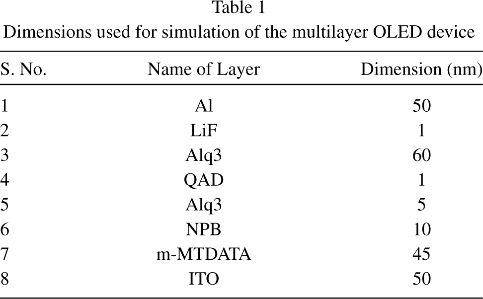
Dimensions used for simulation of the multilayer OLED device
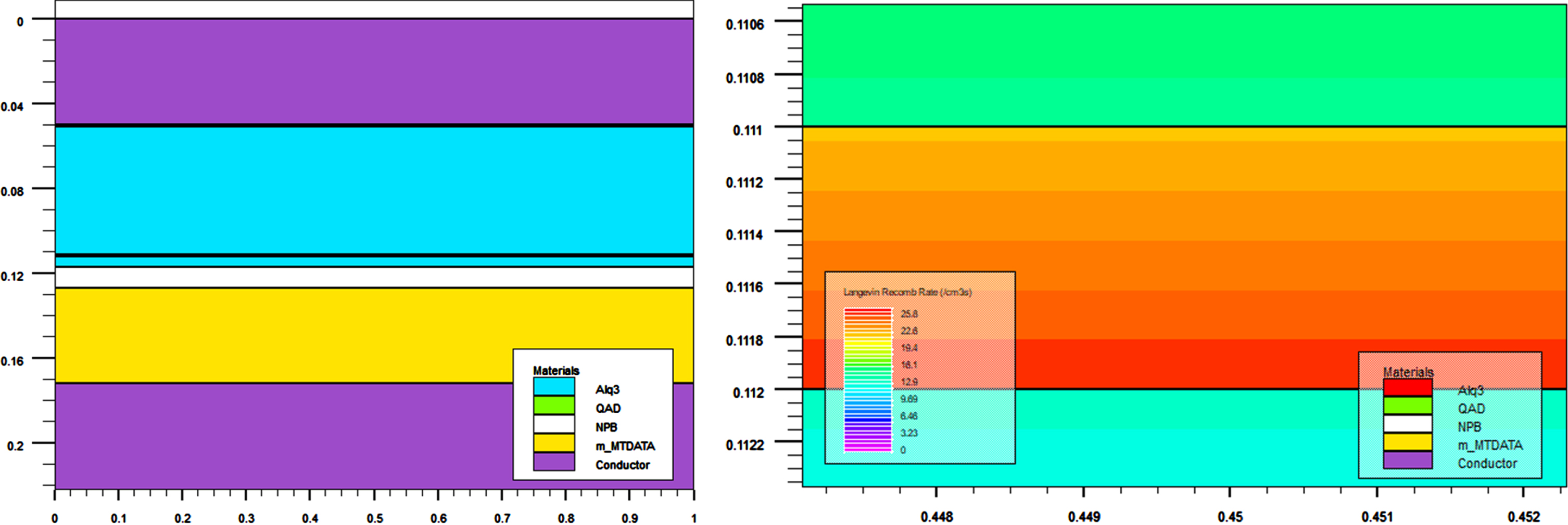
Simulated OLED device structure (a) Proposed Device (b) Langevin Recombination rate.
Since organic semiconductors are characterized by low mobility, the electrons and holes move slowly. The chance for a hole to capture a neighbouring electron will be higher than if they move fast. Langevin gave the theory of such a process. In fact, it is analogous to the direct band-to-band recombination in metallic semiconductors. It means it directly captures electrons and holes as they attract each other by Coulomb force. So, the recombination rate will be proportional to the p-n where p is the hole concentration and n is the electron concentration [12].
One important observation in Langevin recombination is the temperature effect. It increases with temperature. Inorganic binding energy is less than K/q. Thus, the temperature does not impact, but in organic materials, the temperature influences carrier mobility and recombination after e-h pair separation from the excitonic binding effect is predominant [13].
This section is described the deep analysis of multilayer organic light-emitting diodes in three sub-sections Section 3.1, where the effect of current density and anode voltage, thereafter Section 3.2, discusses the outcome of luminescent power and anode voltage and subsequently, Section 3.3, Internal analysis of OLED structure configuration.
Effect of current density and anode voltage
It is well known that the study of current density and as a function of anode voltage is important for the operation of OLED. It is reported that the current density is the rate of injection of carriers in the device [14]. The voltage is the forward operating voltage applied between the anode and cathode of OLED. The higher work function of the anode can reduce the operating voltage as well as increases the current of the device. On the other hand, the lower work function of the cathode can reduce the operating voltage but is not always increasing the device’s current and luminance.
In this work, the current density is plotted as a function of anode voltage for two separated devices in Fig. 3 (a) for the proposed OLED configuration and Fig. 3 (b) for the reported device Negi et al. It is observed that the anode current density in both devices increases monotonically up to 18 V, and beyond this anode voltage, it seems to be saturated. Still, on the other hand, the current density of the proposed configuration has obtained 600 mA/cm2, and Negi et al. reported a current density of 425 mA/cm2. Thus, the proposed device configuration at the QAD thickness of 1 nm obtained a higher current density of 225 mA/cm2 compared to the reported device by Negi et al. at the QAD thickness of 0.1 nm. The possible reason for this increment is the abundance of carriers at a QAD thickness of 1.0 nm which contributes to higher current density [11].

Rate of change of anode current at different values of the anode voltage.
It is well known that luminance power plays a major role in optical devices. This subsection is brief about the effect of luminance power in reference to anode voltage OLED. Since optical power is observed as the intensity of emitted optical light from the surface of optical devices, the major dependency of luminance power is the material types used during the fabrication of optical devices. On the other hand, luminance power alsoshowsitsdependencyonthenumberofexcitonsandappliedvoltageontheOLED. Moreover, the frequency of light also affects the luminance power reported by Negi et al. [11].
In Fig. 4 (a) to (b), the luminescence power is publicised as a function of anode voltage. For the proposed device, in Fig. 4 (a), the seems to be no increment in luminance power between the anode voltage of 0 V to 6 V. Still, from 6 V to 18 V, it keeps increasing continuously; beyond 18 V, it becomes constant. Anode voltage is effective between 6 V to 18 V only for the proposed device. Thus, it can be said that the proposed device is well performed compared to the device reported by Negi et al. [11], which is clearly noticed in Fig. 4(b). The possible reason for the higher luminance power in the curve of Fig. 4(a) is the addition of multiple electron hole-blocking layers with appropriate thickness, i.e., a thicker emissive layer. It improves the luminescent power of OLED because the extra hole-blocking layer directly enhances the recombination rate of electrons and holes at the interface of the emissive layer [13]. Various researchers have also reported their work in organic material-based devices and circuits [13 –42].

Rate of change luminescence power concerning anode voltage (a) Simulated plot of the proposed device (b) Reported OLED device.
To examine the various processes happening in the different layers of device architecture, the internal analysis has been handled by keeping standard performance parameters in this subsection. Furthermore, it helps us to underline the internal processes associated with the physics and behaviour of the device in depth. The internal analysis has proven itself an effective investigation to highlight the methods to enhance the performance of the OLEDs. The internal analysis has been performed by drawing a cutline at the centre of the OLED. It is carried out to observe the effect of various layers of the device on the internal parameters such as total current density, electric field inside the different layers, and electron and hole concentration. These major internal parameters associated with the proposed device have been publicised in Fig. 5 (a-d).

Internal analysis (a) Electric field (b) Total current density (c) Electron concentration (d) Hole concentration.
Finally, in Fig. 5 (a) internal electric field in multi-layered OLED is studied using numerical device modelling. This results in a better comprehension of the operation of the device. This method is used to standard device structure that has received broad attention in the literature. Figure 5 (b-d) total current density, electron concentration and hole concentration results show that the current density of electrons and holes is much higher for electrode injection, particularly charge carriers; further, it reaches zero at the centre part of the OLED device configuration, and they are prevented from reaching the opposite side of the electrode. The density of electrons and holes are very similar to each other. Also, the Electron and hole concentration study focuses on the availability in the vicinity of the emission layer, which better explains the high luminance of the device.
Similar to the internal analysis, a distinct peak is observed in the electric field with a maximum value of 3.6×10⁶ V/cm, slightly lower than the internal analysis. The possible reason suggests that most electrons are bounced back using multiple emissive layers. Moreover, the hole-blocking layer attempts to block holes as much as possible, enhancing the OLED device configuration’s performance. In Table 2, the performance parameter and deflection of the proposed device and reported device have been illustrated for better understanding.
Comparative data for proposed and reported devices

Multilayer OLED has been investigated, and the effect of electrical parameters such as current density and luminance power as a function of anode voltage has been studied in this work. The multi-layered OLED device configuration is critically examined by making vertical cutline methodology to comprehend device operation better. The calculation is made by keeping a QAD thickness of 1 nm. Subsequently, output parameters are evaluated by an analytical model: electric field, total current density, electrons, and hole concentration. The analysis of these internal parameters is termed internal analysis, which highlights the physics and behaviour of the device. These analyses verify the Poole-Frenkel behaviour of mobility-dependent physics of OLED devices. Electron and hole concentration studies focus on the availability in the vicinity of the emission layer, which better explains the device’s high luminance. Langevin recombination has also been observed for the device, which better suggests the recombination rate of electrons and hole pairs. This analysis focuses on the impact of different OLED device architecture layers, making it a more practical device. All simulations are carried out by the Silvaco TCAD tool.
Funding Statement
This research work did not receive financial support.
Conflict of interest
The authors declare that there is no conflict of interest regarding the publication of this paper.
Author Contribution
Authors have made substantial contributions to the conception and design or acquisition of data, analysis, and interpretation of data; have been involved in drafting the manuscript or revising it critically for important intellectual content; and have given final approval of the version to be published. The author has participated sufficiently in the work to take public responsibility for appropriate portions of the content. The author read and approved the final manuscript.
Availability of data and material
The data and material are available within the manuscript.
Compliance with ethical standards
The author declares that all procedures followed were in accordance with ethical standards.
Consent to participate
The author declares their consent to participate in this research article.
Consent for publication
The author declares their consent for publication of the article on acceptance.