



Abstract
BACKGROUND:
Anti-scattering grid has been used to improve the image quality. However, applying a commonly used linear or parallel grid would cause image distortion, and focusing grid also requires a precise fabrication technology, which is expensive.
OBJECTIVE:
To investigate and analyze whether using CO2 laser micromachining-based PMMA anti-scattering grid can improve the performance of the grid at a lower cost. Thus, improvement of grid performance would result in improvement of image quality.
METHODS:
The cross-sectional shape of CO2 laser machined PMMA is similar to alphabet ‘V’. The performance was characterized by contrast improvement factor (CIF) and Bucky. Four types of grid were tested, which include thin parallel, thick parallel, ‘V’-type and ‘inverse V’-type of grid.
RESULTS:
For a Bucky factor of 2.1, the CIF of the grid with both the “V” and inverse “V” had a value of 1.53, while the thick and thick parallel types had values of 1.43 and 1.65, respectively.
CONCLUSION:
The ‘V’ shape grid manufacture by CO2 laser micromachining showed higher CIF than parallel one, which had same shielding material channel width. It was thought that the ‘V’ shape grid would be replacement to the conventional parallel grid if it is hard to fabricate the high-aspect-ratio grid.
Introduction
Radiography has been used for medical purposes such as mammography and simple chest radiography. An image quality and dose administered to the patient exposed to radiation is considered in radiographic diagnosis because it can cause secondary cancer [1]. The main obstacles to the image quality are scattered photons that are generated from the interaction of the incident radiation with matter [2]. If the scattered photons are incident on a detector, the detector count, which should only include the number of primary photons, will be erroneous, as it will include both the primary and unwanted scattering counts. Therefore, an anti-scattering grid of a suitable size is being used in radiography systems in order to reduce scattered photons [3]. In this respect, the choice of an anti-scattering grid becomes important so that it can improve the quality of the image while simultaneously increasing the patient dose only slightly [4].
Fabrication of the anti-scattering grid has been studied and reported were the methods by using lithography [5–8], SU-8 mold [9] and graphite substrate [10]. These freestanding grids had mechanical vulnerability to make it commercialize because the shielding wall was a few tens of μm-thick and its aspect ratio was too high. To avoid it, aluminum- or carbon-fiber-interspaced anti-scattering grids which have higher structural stability than freestanding gird are commercialized. Aluminum and carbon-fiber interspaced grids with two-dimensional pattern are hard to fabricate because they are fabricated by using compression and channel-cutting method, respectively. Actually, two of one-dimensional grids are stack-up to make a two-dimensional grid and hence, it can cause Moiré pattern which is one of the critical artifacts significantly reducing the image quality [11].
The micromachining method for fabrication of the anti-scattering grid requires machinability of few tens of μm with two-dimensional pattern. The direct-write technique on PMMA substrate could make a channel with the width of ∼80 μm [12]. In this study, the two-dimensional anti-scattering grid based on PMMA CO2 laser micromachining technique was suggested in this context. The proposed method has two advantages: The 2-D pattern can be processed without stack-ups. Furthermore, the PMMA is composed mainly of carbon and hydrogen, which reduces the shielding effectiveness of the photon because its density and atomic number is smaller than the other base material such as aluminum or carbon fiber. This study focused on parallel grid instead of focused grid. Parallel grids have been used extensively in general radiographies rather than mammography. In this study, a comparison of the performance between the generic parallel grids and the grid produced by the proposed fabrication method was conducted through the computer simulation. There were a few of studies which included emulation of an X-ray imaging system by using the MCNP code simulation. The characterization of bowtie filter for correction of wide-cone low-dose CT system [13, 14] and the design of a tungsten anti-scattering grid for medium-energy X-ray flash radiography [15] was reported and they were carried out by Monte Carlo based simulation study. A performance test, based on the contrast improvement factor and the Bucky factor, of the suggested anti-scattering grid (so called ‘V-type’ grid) was carried out by using Monte Carlo code MCNP6 [16]. The channel size and depth of the micromachined PMMA was emulated for fabrication of the anti-scattering grid whose test geometry and method were based on the international standard IEC-60627.
Material and methods
Simulation design
Figure 1 (a) and (b) show the overall view of the geometry of the entire simulation for the primary and total photons, respectively. The geometry for the simulation was based on IEC 60627: Diagnostic X-ray imaging equipment – characteristics of general purpose and mammographic anti-scatter grids. It includes the standard method of the test for general purpose and mammographic anti-scatter grids. In Fig. 1, the gray part is the water phantom, which consists of water with a density of 1.00 g/cm3, and the black part is the lead block, which consists of pure lead composed of its natural isotopes with a density of 11.34 g/cm3. The lead block was placed to collimate the primary photons. The arrows toward the bottom in Fig. 1 (a) and (b) indicate the direction of photons from the source. For primary photon transport, the photons had a very narrow angle, whose cosine value was 0.99995 (corresponding to an angle of about 0.573°). For total photon transport, the photons had a relatively wide angle whose cosine value was 0.98894 (corresponding to an angle of about 8.53°), generating both scattered and primary photons. The grid, which is indicated by a thick line, was located at the center part of the bottom, as seen in Fig. 1 (a) and (b). The square at the bottom of Fig. 1 indicates a cylindrical detector of height 1 cm and radius 3 mm.
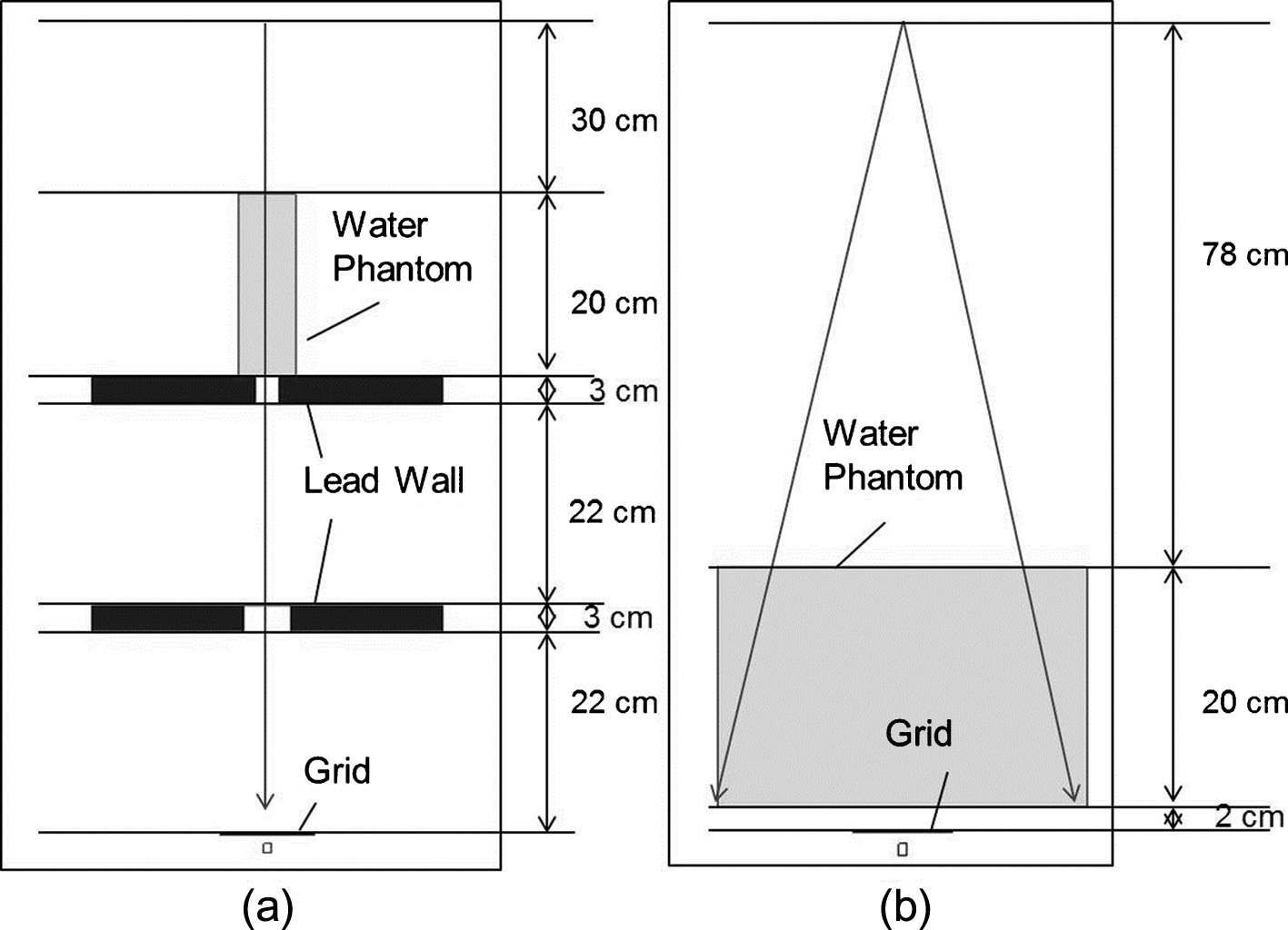
Overall geometry of simulation. (a) Primary photon transportation. (b) Total photon transportation.
The suggested grid was based on the PMMA micromachining technique. It was assumed that a channel was fabricated on the PMMA substrate, and the shielding material was filled in the channel. Figure 2 shows the basic concept of the grid where the white and black parts indicate PMMA and lead, respectively. An anti-scattering grid is a lattice-shaped board that consists of shielding materials and interspace materials between the shielding. Because the anti-scattering grid also blocks the primary photons, the primary photon count is decreased, which can result in a reduction in the radiation image contrast. A scattered photon is defined as a photon that is scattered from the target (or patient) and has different and several random directions compared to a primary photon, where a primary photon is defined as a photon from the radiation source without any scattering. The photons from the source enter the target. Some photons are scattered and absorbed by the interspace and shielding material, and others pass through it. The ratio of scattered and primary photon could be characterized as scatter-to-primary ratio (SPR) and it was changed whether the anti-scattering grid was used or not. For previous study, the SPRs of the grid produce by electroplating and without grid were 0.0964 and 0.1594, respectively, and the grid reduced the SPR by 30.52% [17]. The absorbed photons and those that pass through are not obstacles in terms of the image quality. Only the scattered photons, which may have low energy, need to be reduced for enhancement of the image quality.
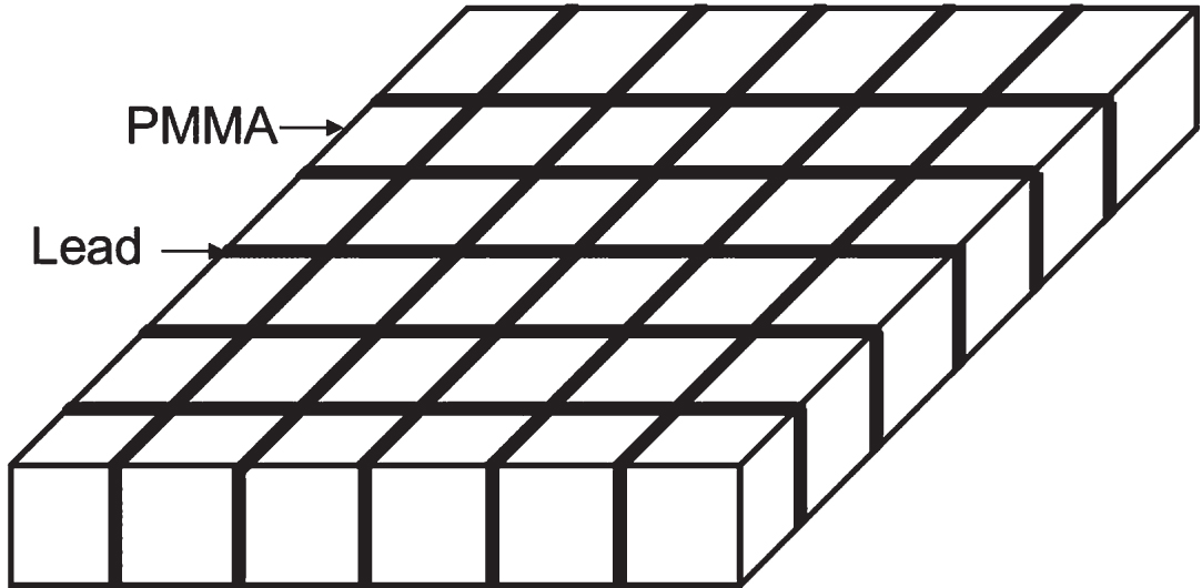
Conceptual scheme of a PMMA based grid. Black line represents the shielding material, lead, and white block represents the interspace material, PMMA.
Two physical assumptions for the design of the grid are as follows: The scattered photons might lose their energy because of the interspace material at the bottom of the grid; therefore, the shielding material at the bottom can be relatively thin. If the shielding material has a V-shaped cross section, the top of the shielding material is thick and the bottom is relatively thin. The scattered photons, which are scattered at a higher angle, might be directed to the top of the shielding material and those with a lower angle to the bottom of the shielding material. The photons scattered at a higher angle have a lower energy, where the top of the shielding material can be thin.
Under these assumptions, the shielding material has a V- or A-shaped cross section. The “V” and inverse “V” shapes are in accordance with the fabrication characteristics of PMMA, because the PMMA fabricated by CO2 laser has a V-shaped cross section.
Figure 3 shows the cross-sectional view of the four types of grids tested, the thick parallel type, thin parallel type, “V” type, and inverse “V” type. In Fig. 3, the black part indicates the shielding material, and the gray part, the interspace material. In Fig. 3 (a), the distance between the shielding walls was 60 μm and the thickness of the shielding wall was 20 μm; hence, the line density of the shielding wall was 125 lines cm-1. In Fig. 3 (b), the thin parallel-type grid with a relatively thin shielding wall was tested for comparison with the “V” and inverse “V” types with the same mass of shielding material. For the thin parallel type, the distance between the shielding walls was 70 μm and the thickness of the shielding wall was 10 μm. The distance between the shielding walls was increased to make the line density of the shielding wall constant. In Fig. 3 (c) and (d), the distance between the walls and the thickness of the wall for both the grids with “V”- and inverse “V”-shapes were 60 μm and 20 μm, respectively.

Cross sectional view of the tested grid. (a) Thick parallel type (b) Thin Parallel type (c) “V”-type (d) “Inverse V”-type.
The indicators of the performance of the grids are selectivity, contrast improvement factor (CIF), and the Bucky factor [18]. Equation (1) and (2) shows the definition of Bucky factor and CIF.
The photon flux at the top of the detector (Ip or It) was obtained from simulation with and without the grid. The transmission ratio of the primary photons (Tp) and total photons (Tt) was calculated as the ratio of the data acquired with and without the grid. The consideration of the scattered photons was not included because only the CIF and Bucky factor were considered for comparing the performance of the grid, where CIF was the ratio of Tp and Tt. This factor is a measure of how many primary photons entered the detector relative to the total photons. A high CIF means that there are many primary photons among the total photons. The CIF is plotted as a function of the change in the Bucky factor. The grid with the higher performance has a higher CIF for the same Bucky factor, where the slope of the CIF vs. the Bucky factor increases and a relative shift toward the left is seen. The simulation was conducted for varying grid ratio from 3 to 7, which was defined as the ratio of the height of the grid (or shielding wall) to the distance between the walls.
Figure 4 shows the result of the calculated CIF as a function of the Bucky factor. The CIF was linearly proportional to the Bucky factor, implying that the grid ratio had no effect on the grid performance, where the grid performance meant both a reduction of the patient dose and an improvement in the image quality. Grid ratios of 3, 4, 5, 6, and 7 were used for each type of grid. The performance of the grid becomes independent of the grid ratio because the relation between the CIF and the Bucky factor is linear. A high slope in the CIF vs. Bucky factor graph means that a higher contrast image can be obtained when the same amount of radiation is applied to the patient. Therefore, the larger the slope of the plotted line according to the difference in the grid ratio in Fig. 4, the better the performance of the grid. Clearly, the thin parallel-type grid showed a higher performance than the thick parallel-type grid (Fig. 4), here the density of the shielding wall (or lattice cell) was the same for the grids of each type. When the Bucky factor was 2.3, the CIF was 1.79 and 1.51 for the thin and thick parallel-type grids, respectively (Fig. 4). The thin parallel-type grid showed about 19% higher CIF for the same Bucky factor of 2.3. For a higher grid ratio, the difference became larger, as shown in Fig. 4. The CIF is related to the transmission rate of the primary photons. The increase in the transmission rate of the primary photons was higher for the thin parallel-type grid than for the thick one, whereas the grid ratio increased because the amount of shielding material increased faster for the thick parallel-type grid than that for the thin one, where the shielding material contributed to the absorption of the primary photons.
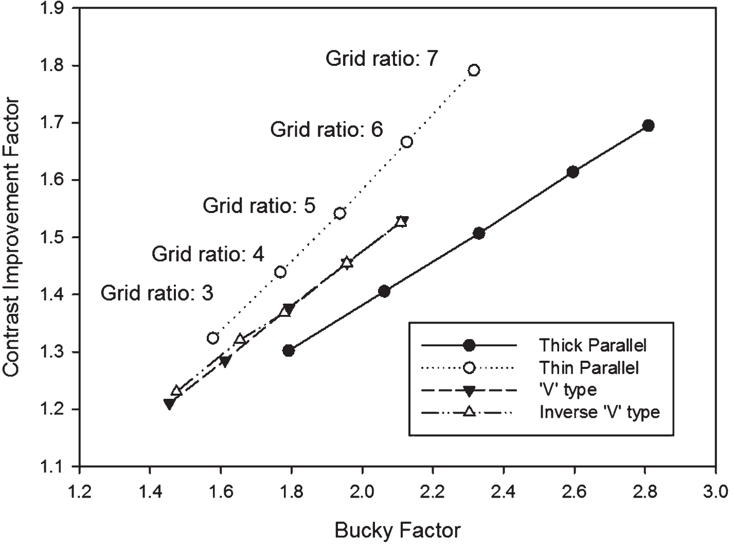
Bucky factor vs. Contrast Improvement Factor for grids of thick parallel, thin parallel, “V” and inverse “V”-type on the different the grid ratios (bottom left: 3 and top right: 7).
The magnitude of CIF for both the “V” and the inverse “V”-type plots was relatively low for the same grid ratio, and ranged between those of the thick and thin parallel-type grids (Fig. 4). For a Bucky factor of 2.1, the CIF of the grid with both the “V” and inverse “V” had a value of 1.53, while the thick and thin parallel types had values of 1.42 and 1.65, respectively. The thin parallel-type grid had about 8% higher CIF and the thick parallel-type grid showed about 7% lower CIF for the same Bucky factor. In terms of performance, the higher slope in the CIF vs. Bucky factor graph, the higher performance of the grid. The “thin-parallel’ showed the best performance, however, there was no study of the fabrication of the grid with shielding wall thickness of 10 μm because the channel width is too small. For the same channel width or aspect ratio, the proposed design of the grid (‘V’ or inverse ‘V’ type) shows the better performance than the parallel grid. This meant that the grid could have higher performance at the same aspect ratio but lower performance at the same mass or volume of shielding material.
In Fig. 4, the inverse “V”-type grid had higher performance than the “V”-type grid for a low grid ratio because the CIF of the inverse “V”-type was higher than of the “V”-type with same Bucky factor. It was thought that almost all the scattered photons were removed by the shielding wall at a high grid ratio. However, the population of the surviving scattered photons at the bottom of the grid was larger for a lower grid ratio than for a higher grid ratio. Therefore, it was understood that the inverse “V”-type grid had a thicker shielding wall at the bottom, and the shielding capability for the scattered photons at the bottom was better than that of the “V”-type. From the definition of CIF (Tp over Tt), the transmission ratio of the primary photons was found to be the most important factor for the performance of the grid, requiring a minimal blocking of the primary photons, where a high aspect ratio of the shielding wall was additionally required. However, if the aspect ratio of the shielding wall is the same, the inclined shape (or “V” shape) has higher performance because the “V” or inverse “V”-type grid blocks less primary photons. This justifies fabricating a grid on a PMMA substrate because the channel formed is inclined. Two kinds of aspects needed to be solved were found in this study: injection of the shielding material and minimization of the channel width. In terms of injection, several obstacles for injecting a shielding material in the etched channel on PMMA could exist. The channel width of a CO2 laser micromachined PMMA was still large, with the width at the top of the channel being 100 μm.
It was thought that the ‘V-type’ grid was easier to fabricate than the thin parallel one. The PMMA would be sufficiently binding with metal because it has been used in metal injection molding (MIM) system [19]. However, two points should be clear to make the fabrication of the anti-scattering grid possible. First of all, the power of laser should be stable to keep the channel width constant. Secondly, the thermal durability of PMMA is concerened because the melting point of the PMMA and pure lead was 160°C and 327.5°C, respectively. To overcome this, a metal injection in the 50-μm patterned PMMA with rapid cooling technique [20] and electroplating on the PMMA with high aspect ratio [21] is considered for building up the shielding wall. These techniques could be considered as a soulution of shielding wall injection in the PMMA channels with direct-write using laser.
Conclusion
The performance of a CO2 laser micromachining-based PMMA anti-scattering grid was analyzed using MCNP code simulation. It was determined that “V” and inverse “V”-type grids had a higher performance compared to the parallel-type grid for the same aspect ratio of the shielding wall, whereas the parallel-type grid had a higher performance for the same mass (or volume) of shielding material. If a thin shielding wall is difficult to fabricate, the choice of a “V” shape as a shielding wall was thought to be appropriate, taking into consideration the difficulty in fabricating a thin shielding wall. It was verified that the thickness of the shielding wall was one of the most dominant factors for the fabrication of a high performance anti-scattering grid.
Footnotes
Acknowledgments
This work was supported by the Material/Part Technology Development Program, (10046623, Development of focusing X-ray grid with 250,000 pixels/inch2 by micromachining) funded by the Ministry of Trade & Energy (MI, Korea) and by Industrial Technology Innovation Program (2016520101340, Real-time Underwater Tritium Monitoring Technology by Electrolysis) funded by the Korea Institute of Energy Technology Evaluation and Planning (KETEP, Korea).