
Abstract
The influence of fast neutron irradiation on the structure and spatial distribution of Ge nanocrystals (NC) embedded in an amorphous SiO2 matrix has been studied. The investigation was conducted by means of laser Raman Scattering (RS), High Resolution Transmission Electron Microscopy (HR-TEM) and X-ray photoelectron spectroscopy (XPS). The irradiation of Ge-NC samples by a high dose of fast neutrons lead to a partial destruction of the nanocrystals. Full reconstruction of crystallinity was achieved after annealing the radiation damage at 8000C, which resulted in full restoration of the RS spectrum. HR-TEM images show, however, that the spatial distributions of Ge-NC changed as a result of irradiation and annealing. A sharp decrease in NC distribution towards the SiO2 surface has been observed. This was accompanied by XPS detection of Ge oxides and elemental Ge within both the surface and subsurface region.
1. Introduction
Since the early 1990s, samples of Si and Ge nanocrystals (NC-Si, Ge-NC) embedded in a silicon dioxide (SiO2) matrix have attracted much interest due to strong visible photoluminescence at room temperature [1,2]. Additional electrical studies performed on these NC have revealed charge retention properties [3–14], suggesting the future incorporation of such structures in silicon-based electronic technology such as optoelectronic and microelectronic devices [5, 6, 8–16]. It has been shown [17, 18] that Ge-NC's smaller band-gap makes it a more suitable material than NC-Si for silicon-based technology. This property has made Ge-NC the promising candidate for the creation of a new generation of nano-scale optoelectronic devices. In this respect, investigation of the ability of the material to withstand different destructive influences is important for the design of semiconductor devices that can normally operate in a radiation-rich environment.
Early work investigated the role of ion-induced damage to the structure of Ge-NC. It was observed that Ge-NC are highly sensitive and become amorphous at a Si+ ion dose of 5×1013 cm−2 [19]. Irradiation by high energy neutrons in a nuclear reactor leads to different structure and distribution of the radiation damage, because neutrons are not charged and have significantly lighter mass when compared to ions. Clash with fast neutrons with energy up to several MeV causes displacement of atoms in the lattice in cascades, which produce radiation damage in the form of nanometer size amorphous clusters, impurity-vacancy complexes, etc. [20]. These directly contribute to the destruction of the optical and electrical performance of bulk Si and Ge-based devices (such as diodes and hetero-junction bipolar transistors (HBTs) [21]). MOS (Metal Oxide Semiconductor) devices are known to withstand displacement-caused degradation only up to integral dose of 1015 neutrons/cm2 [22]. In this investigation, Ge-NC samples were subjected to a much higher dose of 1020 neutrons/cm2.
In addition, besides the radiation damage due to fast neutrons, absorption of slow (thermal) neutrons leads to transmutation of different isotopes of Ge into impurities due to nuclear reactions. For example, 74Ge transforms to 75As (donor impurity), 70Ge into 71Ga (acceptor impurity) and 76Ge into 77Se (deep double donor impurity). This process is called “neutron transmutation doping” (NTD). Concentration of NTD introduced impurities is proportional to abundance of the given isotope in the natural Ge composition, cross-section of the absorption of thermal neutron and the integral dose of thermal neutron flux [20, 23]. Transmutation processes are accompanied by emission of γ-quanta and β-particles, which can, in principle, contribute to the radiation damage as well. Investigation of bulk NTD-Ge showed that almost all radiation damages are removed after annealing of neutron irradiated samples at 4000C [24].
The Ge-NC samples investigated in this work were obtained in cooperation with the group from Sichuan University, People's Republic of China. Investigations of this group [25–28] were focused on the influence of 75As impurities introduced by NTD into samples prepared by ion implantation of 74Ge into SiO2 matrix. The aim of this work is to investigate the structure, size and spatial distribution of Ge-NC in samples after all steps of treatment: fabrication, neutron irradiation and radiation damage annealing.
2. Experimental details
Our samples underwent five stages of treatments described below; at each stage of treatment a control sample was kept.
The Ge-NC samples were prepared using 74Ge+ ion-implantation into a 500 nm thick amorphous SiO2 layer, deposited on a silicon substrate with <100> oriented surface. The details of the ion-implantation are documented in [25, 26]. The Ge+ ions were accelerated to 150 keV, with a dose of 1×10¹⁷ ions/cm2. These samples were labeled as “implanted”. A second treatment was conducted on the implanted samples by annealing at 8000C for 1h. As a result, the randomly distributed Ge atoms formed nanocrystals (NC) [29]. These samples were labeled as “Ge-NC”. The third process consisted of subjecting the Ge-NC samples to an intensive neutron irradiation in a research nuclear reactor, with the integral dose of 1020 neutrons/cm2, and subsequently labeled as “irradiated”. The neutron irradiation was performed at room-temperature. After irradiation, a fourth group consisting of irradiated Ge-NC samples was annealed at 6000C for 1h to remove the radiation damage. These samples were labeled as “semifinal”. The remaining samples were annealed a second time at 8000C for 1h. This fifth group of samples was labeled as “final”.
It should be noted that to distinguish between defects, resulting from the destruction of the lattice by the fast neutron irradiation, and elements and defects that appear due to transmutation and the presence of impurities, half of the irradiated samples were irradiated within a cadmium (Cd) box, which was used as a shield from the slow (thermal) neutrons. As a result, samples irradiated within a Cd box were subjected only to the influence of fast neutrons, while samples irradiated outside a Cd box were subjected to the flux of both fast and slow neutrons. We note that in our study of Ge-NC structure, no significant differences were found between the samples irradiated inside and outside a Cd box, therefore in the following, we will not distinguish between these two types of sample. The influence connected with transmutation doping may be detected in a study of the electrical and optical properties of the samples, which is outside the scope of this manuscript.
Measurements of Raman scattering (RS) and High Resolution Transmission Electron Microscopy (HR-TEM) are usually used to confirm the crystalline structure. Crystalline Ge is characterized by the Raman peak centered at approximately 300 cm−1, which corresponds to the optical phonon frequency in bulk Ge crystals [30]. Measurements of HR-TEM images enable the examination of fine details of the NC structure. In addition to the crystalline structure analysis, the surfaces of the samples were analyzed by X-ray photoelectron spectroscopy (XPS).
RS spectra were measured with a Raman microscope LabRam HR and were taken in the back-scattering geometry at room-temperature using a 514.5 nm laser source for excitation. HR-TEM images were obtained using the 200 kV JEOL, JEM 2100 HR-TEM (LaB6) integrated with a scanning device comprising annular dark-field and bright-field detectors and with a Noran System Six EDS (energy dispersive X-ray spectroscopy) system for elemental analysis. For cross-section imaging, HR-TEM samples were prepared by a focused ion beam (FIB) lift-out technique. XPS measurements were carried out on AXIS HS Kratos Analytical electron spectrometer system. The spectra were acquired using a monochromatic Al-K (1486.6 eV) X-ray source.
3. Results and discussion
3.1 Initial samples (before neutron irradiation)
Curve a in Fig. 1 shows RS spectra in the implanted sample, where Ge atoms do not yet form nanocrystals. One can see a broad asymmetric unstructured band which can be attributed to separate Ge atoms or amorphous nano-clusters [29, 33].
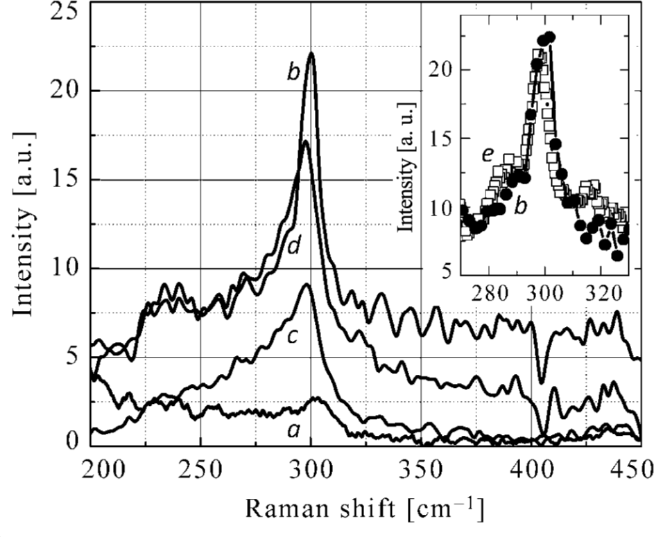
Raman spectra of (a) implanted, (b) Ge-NC, (c) irradiated and (d) semifinal samples; inset displays RS around 300 cm−1 for Ge-NC (b) and final (e) samples.
Fig. 2a shows bright-field HR-TEM cross-sectional image of a Ge-implanted sample, where Ge atoms have not yet formed nanocrystals. In bright-field mode it is possible to distinguish between the Ge clusters and the SiO2 matrix due to the contrast of the image, i.e. regions with Ge atoms appear darker while the SiO2 matrix appears brighter.

HR-TEM cross-section of (a) implanted (b) Ge-NC, (c) irradiated and (e) final samples. The dashed line indicates the surface of the samples covered by Pt which is needed for TEM cross-section preparation.
Nonappearance of NC is confirmed by the absence of a diffraction pattern.
Conforming to the SRIM simulation (Stopping and Range of Ions in Matter simulation) [32], the projection range and straggle (half-width of the distribution) for Ge ions with energy of 150 keV implanted in SiO2 are approximately 100 ±5 nm and 30 nm, respectively, which concur with the experimental observation (Fig. 2a).
In order to form nanocrystals, implanted samples were annealed at 8000C. Formation of Ge-NC was confirmed by the appearance of the main RS peak, centered at 300 cm−1 (see curve b in Fig. 1) which is characteristic of crystalline Ge. The absence of a significant shift of the Raman peak from 300 cm−1 indicates that no effects connected with stress [33] or quantum confinements [34] are observed. In addition, crystalline structure was observed in the enlarged HR-TEM image in the form of equidistant lattice planes (Fig. 2b). The HR-TEM image shows that Ge-NC regions have an almost spherical shape with a diameter of approximately 2-10 nm. Inspection of the image reveals a correlation between the diameter and the depth of NC below the SiO2 surface: within the projection range (100 nm), where the density of the implanted Ge atoms is maximal, the average diameter of Ge-NC is also largest and symmetrically decreases on both sides.
The composition of Ge-NC was studied by an accompanying investigation of selected area electron diffraction (SAED) pattern of the Ge-NC layer inside the SiO2 matrix and live fast Fourier transform (FFT) performed on an HR-TEM image of a single NC (Fig. 3). In SAED measurements, the d-spacing between planes (111), (022) and (222) was found to be 3.2, 1.95 and 1.67 Å ±0.04 Å, respectively. In the case of FFT the d-spacing between planes (111), (022) and (−111) was found to be 3.3, 2.0 and 3.4 Å ±0.06 Å respectively.
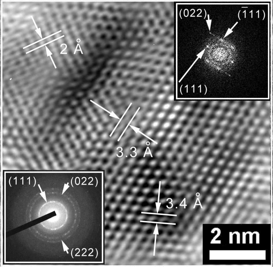
Enlarged (processed) HR-TEM image of a single NC, live fast Fourier transform (FFT, upper right inset) calculated from the HR-TEM image and selected area electron diffraction (SAED, bottom left inset) of the Ge-NC layer inside the SiO2 matrix. The d-spacing of the planes, as calculated by live FFT, are displayed in the HR-TEM image.
Using both diffraction and live FFT, it is possible to conclude that the crystals consist of Ge and are not a mix of any compound of Ge. It has also been observed that different crystallographic orientations coexist in some single NC, which can be explained by the existence of more than one nucleation center that serve as seeds forming each Ge-NC. That is, nucleation centers form small sized NC during the annealing process. These NC aggregate toward one another, and once they come into contact their lattice planes start to adjust at the interface.
3.2 Influence of fast neutron irradiation and annealing
Part of Ge-NC samples were irradiated by an intensive neutron flux (with energy up to a few MeV) in a research nuclear reactor with integral dose of 1020 neutrons/cm2. As a result of this irradiation, a RS peak was decreased and broadened (curve c in Fig. 1). This can be explained by the destruction of some NC and their transformation from Ge nanocrystals into amorphous clusters. However, RS peak did not disappear. This indicates that part of the Ge-NC has survived even after the high dose of destructive irradiation. The existence of remaining Ge-NC in irradiated samples was confirmed by HR-TEM image (Fig. 2c). Taking into account that the dose of irradiation was five orders of magnitude larger than the one which destroyed the devices made from bulk Ge and Si [21], one can conclude that this material shows potential for devices assigned to work in extreme conditions, such as a radiation-rich environment.
In Fig. 1, curves d and e show the influence of the annealing of irradiated samples on the RS spectrum. For bulk Ge, disappearance of radiation damage induced by fast neutrons is achieved after annealing at 400-4500C [24]. For Ge-NC, however, annealing even at 6000C leads only to a partial reconstruction of the RS peak (curve d in Fig. 1); annealing at 8000C is needed for full reconstruction of the initial RS peak (inset in Fig. 1). This phenomenon can be explained by the following: In irradiated bulk Ge, the destroyed areas are surrounded by a monocrystalline matrix that serves as a seed for recrystallization. In our samples, the destroyed areas are surrounded by amorphous SiO2 which cannot promote the process of crystallization. As a result, the same temperature (8000C) which was needed for the initial formation of Ge-NC after ion-implantation was still required in order to recover the crystalline structure after the fast neutron irradiation.
However, the reconstruction of crystallinity was not accompanied by the rebuilding of the initial space distribution of Ge-NC (compare Fig. 2b and 2e). It is evident that the spatial distribution of nanocrystals became asymmetric - the increased average size still corresponds to the center of the projection range, while towards the SiO2 surface, the density of NC falls more rapidly.
The asymmetry in the space distribution of Ge-NC after neutron irradiation and annealing was also confirmed by an EDS line scan of the final sample (Fig. 4). The EDS elemental mapping (line scan profile) provides information on the chemical composition of very small volumes of material by plotting the abundance of an element with distance along a line (counts vs. distance).

STEM image including an EDS line scan profile of a final sample. The curves display the abundance of elements with distance along the line (counts vs. distance along the line). The curves corresponding to elemental Ge and Si are shown.
Fig. 4 shows the STEM image of the cross-section of a final sample. The image clearly shows the asymmetry in distribution of Ge atoms inside the SiO2 matrix.
This asymmetry can be explained by the influence of the near SiO2 surface which attracts Ge atoms during the final annealing. XPS measurements were performed to check the assumption regarding the enhanced diffusion of the Ge atoms towards the surface region upon the annealing of the irradiated samples. The results are shown in Fig. 5.

High resolution X-ray photoelectron spectroscopy (XPS) scans of Ge 3d peaks in Ge-NC (a) and final (b) samples. The 33.4 eV peak attributed to Ge oxides (Ge 3d GeO2), and a less pronounced peak at 29.4 eV corresponding to elemental Ge are evident only in the final sample.
It is seen that in Ge-NC samples, the surface region is Ge free, while only after neutron irradiation and a second annealing at 8000C, a peak appears at 33.4 eV, attributed to Ge oxides (Ge 3d GeO2), and a less pronounced peak at 29.4 eV corresponds to elemental Ge [35].
The presence of both Ge oxides and elemental Ge confirms the assumption that the asymmetry in the distribution of Ge-NC is due to diffusion of Ge atoms towards the surface during the second annealing from 6000C to 8000C.
4. Conclusions
Investigation of Ge-NC samples embedded in an amorphous SiO2 matrix and subjected to irradiation by the neutron flux in a nuclear reactor demonstrates that part of the Ge-NC survives even after the exposure to an extremely high dose of irradiation (up to 1020cm−2). This may indicate that if some optical or electrical properties of Ge-NC-based material are connected with existence of Ge nanocrystals, then this material may show potential for the fabrication of devices working in extreme conditions. In the case of NC, annealing of radiation damage needs higher temperatures than that in bulk Ge. After the annealing of radiation damage, crystallinity is recovered, but the space distribution of Ge-NC becomes asymmetric due to the enhanced diffusion of Ge atoms towards the SiO2 surface.
Footnotes
5. Acknowledgments
We are thankful to J. M. Lazebnik for his help in sample irradiation. We also thank M. Talianker, A. Belostotsky and Y. Fleger for technical assistance. I. S. thanks the Erick and Sheila Samson Chair of Semiconductor Technology for financial support. This work was partly supported by the Israeli-China grant 3-405.