
Abstract
As a branch of laser powder bed fusion, selective laser sintering (SLS) with femtosecond (fs) lasers and metal nanoparticles (NPs) can achieve high precision and dense submicron features with reduced residual stress, due to the extremely short pulse duration. Successful sintering of metal NPs with fs laser is challenging due to the ablation caused by hot electron effects. In this study, a double-pulse sintering strategy with a pair of time-delayed fs-laser pulses is proposed for controlling the electron temperature while still maintaining a high enough lattice temperature. We demonstrate that when delay time is slightly longer than the electron-phonon coupling time of Cu NPs, the ablation area was drastically reduced and the power window for successful sintering was extended by about two times. Simultaneously, the heat-affected zone can be reduced by 66% (area). This new strategy can be adopted for all the SLS processes with fs laser and unlock the power of SLS with fs lasers for future applications.
Introduction
Selective laser sintering (SLS), a branch of laser powder bed fusion, is one of the most popular additive manufacturing (AM) techniques for fabricating a wide variety of materials.1–4 SLS uses high power lasers to sinter particles of powder form into solid parts. For many applications, metal nanoparticles (NPs) are used in SLS for their lower melting temperature compared with bulk, as well as highly controllable sizes and shapes. Successful examples include silver NPs for electric circuits, 5 copper NPs for micropatterns in interconnects on transistor IC chips, 6 tungsten NPs for aerospace parts or nuclear fusion reactor, 7 and titanium and ceramic NPs for biocompatible bone grafting.8,9 Current SLS usually uses continuous wave (CW) or nanosecond (ns) laser pulses to sinter micron size metal particles.
The uncontrolled heat-affected zones (HAZs) of CW and ns pulses result in severe problems in the finished products, such as high porosity, rough surface, and large residual stress.10,11 The problem becomes even more severe when substrates are heat sensitive, such as polymers. SLS with femtosecond lasers (fs-SLS) has unique advantages due to its ultrashort pulse width and highly localized HAZ, including but not limited to the following: high precision and accuracy at submicron scale, rapid cooling rate, less oxidation, reduced residual stresses, and so on.1,12 Furthermore, the high peak power makes fs-SLS exceptionally effective in sintering materials with high melting temperature, such as ceramics; and the extremely localized HAZ also makes it possible to write electrical circuits directly onto flexible substrates without damage.
Despite these advantages, sintering of metal NPs with fs lasers is challenging due to strong ablation of NPs, and successful sintering is reported in only a few studies.13–15 In our previous work about comparing the sintering results of Cu NPs with CW, ns and fs lasers, on an aluminum substrate, sintering window with fs laser (3.2–44 W/cm2) is much narrower than that with ns laser (12.8–331 W/cm2) and CW laser (74,603–323,283 W/cm2), even though fs laser can sinter the Cu NPs with much less power consumption. 16 The narrow sintering window with fs laser due to strong ablation makes it difficult to apply fs-laser for wide-range applications.
Interaction between fs laser and metals is briefly described here. Once electrons in metals absorb photons, they redistribute momentum through electron-electron (e-e) scattering and become a hot electron gas. These hot electrons possess an extremely high temperature (Te), which is usually 103–104 K. They will then travel ballistically or superdiffusively out of the illuminated area, and at the same time, pass the energy to the lattice through electron-phonon (e-ph) coupling. When using a CW or ns laser to sinter metal NPs, only thermal effects are expected because the laser duration is much longer than e-ph coupling time. Fs-laser can remove materials without causing any thermal damage, through hot electron blast or coulomb explosion effects.17–19 When fs-laser intensity is high enough, hot electrons of high density are created within the optical penetration depth.
The high density and large gradient of hot electron gas can induce a strong blasting force, which is proportional to the hot electron temperature squared (
Hot electron effects (blast and Coulomb explosion) are beneficial in fs ablation of bulk materials and have been extensively studied for advanced manufacturing.22–24 Hot electron effects can ablate metal NPs before the e-ph coupling finishes, which prevents sintering, and hence are the bottlenecks for achieving good sintering. The main challenge is about how to suppress these hot electron effects and promote energy transfer from electrons to the lattice.
Since the hot electron effects depend on hot electron temperature (
This new strategy can be conveniently adopted for all the SLS processes with fs laser and unlock the power of fs-SLS for future AM applications. Even though this concept of double-pulse sintering is demonstrated only for a single-layer sintering, which is sufficient for applications such as direct-writing of electrical circuits on flexible substrates, 5 3D products can also be manufactured through repeating the spin-coating and fs-laser sintering processes layer-by-layer. 25
Background and Experimental Setup
Laser-material interaction described with two-temperature model
Figure 1a depicts the major steps of the energy transfer path after a metal NP absorbs photons from a fs-laser pulse. 26 First, electrons of a large density are excited collectively and generate plasmon resonance, where electrons oscillate coherently (in phase with each other). This phenomenon has been studied extensively in chemistry and biology fields.27–29 Plasmon resonance only lasts for about 10 fs, which will not be considered here. Hot electrons reach an equilibrium state through e-e scattering. In metals, this process usually takes about ∼100 fs. When metal NP size is small, hot electron diffusion is limited within a small volume, and surface scattering becomes important. Next, energy is transferred from this high-temperature hot electron system to lattice through e-ph coupling, which is about several to tens of ps in noble metals.
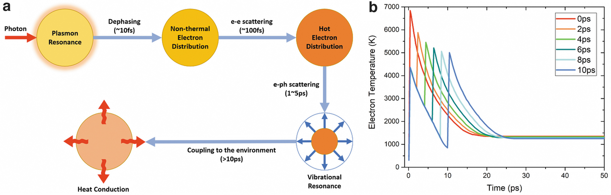
Coherent vibrations from radial breathing modes are also observed in this process.30–32 Finally, the heated NPs will exchange energy with the environment through heat diffusion. In NPs, the laser fluence threshold for hot electron blast and Coulomb explosion may be much lower because of their large surface area and small volume. Successful sintering requires that the lattice temperature (Tl) reaches a threshold for partial/full melting. Metal NPs can be ablated very easily and the window of experimental parameters to achieve sintering is extremely narrow.
When simulating fs-laser interaction with metals, commonly used is a two-temperature model (TTM) that includes two coupled temperature equations for hot electron (Te) and lattice (Tl).33–35 Figure 1b plots the electron temperature computed with TTM, using two fs laser pulses with varying delay time. The laser fluence is selected to be 1510 J/m2 so that the lattice temperature is high enough for sintering. The melting temperature for bulk Cu is about 1358 K and about 1351 K for 100 nm Cu particles. At 0 ps delay time, where the two pulses overlap in time, which is equivalent to the case of single pulse with doubled energy, Te quickly rises up to 6900 K, and relaxes to around 1350 K at about 20 ps.
With a longer delay time, there are two peaks in the Te plot, which are caused by the first pulse and the second pulse. Due to the first pulse, Te rises to around 4400 K and starts to decay. The following second pulse heats up the electrons again to have the second peak. After the second peak, the Te decreases until the temperature becomes the same with the lattice temperature. So, with proper delay time, the highest Te can be controlled to be lower than 5000 K, significantly lower than the around 7000 K with single pulse. Figure 1b only simulates the case of a single Cu particle. In powder bed, a similar effect is expected, even though the values of Te could be different.
Sample preparation and experimental setup
The Cu inks used in this study are purchased from Applied Nanotech, Inc., with a nominal diameter of 100 nm. This size is comparable with the electron mean free path (∼40 nm 36 ) and nanoscale heat transport becomes important. We measured the effective thermal conductivity of 100 nm Cu NPs with transient thermoreflectance technique, 37 and found that the thermal conductivity is as low as 18.5 W/mK, much smaller than the bulk value of 398 W/mK. The substrate is a glass deposited with a 50-nm gold film. Cu NPs film is prepared on the substrate with spin coating (WS-650Mz-23NPPB; Laurell, 1000 rpm for 1 min). The sample is then dried on a hot plate at 100°C for 30 min to remove the organic solvent. The final sample geometry is illustrated in Figure 2b. The thickness of Cu NPs film is about 1 μm.
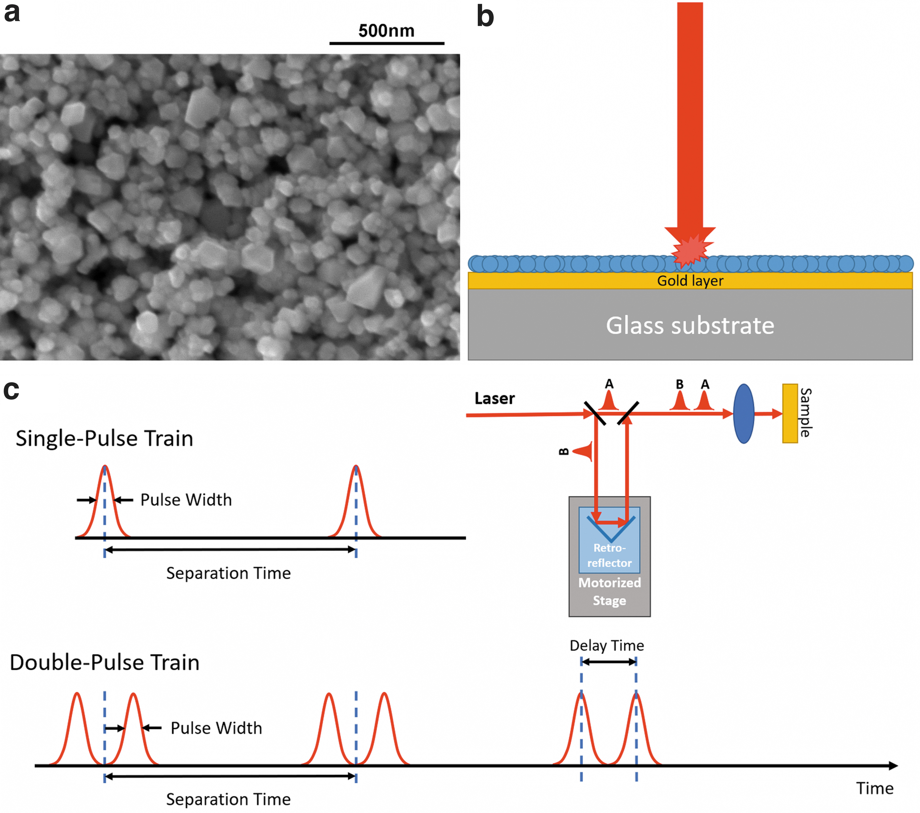
Figure 2c shows the schematics of generating a double-pulse train. One laser beam is split into two branches, A&B. The optical path of the B branch is controlled with a motorized stage. The difference of optical paths between A&B converts to the difference of arrival time of A&B at the sample (delay time), for example, 3 μm corresponding to 10 fs. A&B are recombined at the second beam splitter before being focused onto the sample. For fs laser, there is another term called separation time, which is determined by the inherent repetition rate of the laser and should not be confused with the delay time between A&B. Our laser source is a Ti:Sapphire Regenerative Amplifier (Spitfire Ace, Spectra-Physics) with central wavelength of 800 nm, pulse width 35 fs and repetition rate of 5 kHz (corresponding to a separation time of 200 μs).
The intensities of A&B can be tuned individually with a pair of half wave plate/polarizer so that their intensities are roughly the same. Both A&B pulses are p-polarized. A mechanical shutter is used to control how many pulses can arrive at the sample position. The exposure time of shutter is set to be 0.02 s for all our experiments, which allows 100 pulses to pass by. (Details of experimental setup in Supplementary Data.) Laser spot size is around 27
Results and Discussion
With our home built sintering station, we conducted spot sintering and line sintering with fs double-pulse train at different delay times and compared the results with cases of single-pulse train.
Scanning electron microscopy images of spot sintering
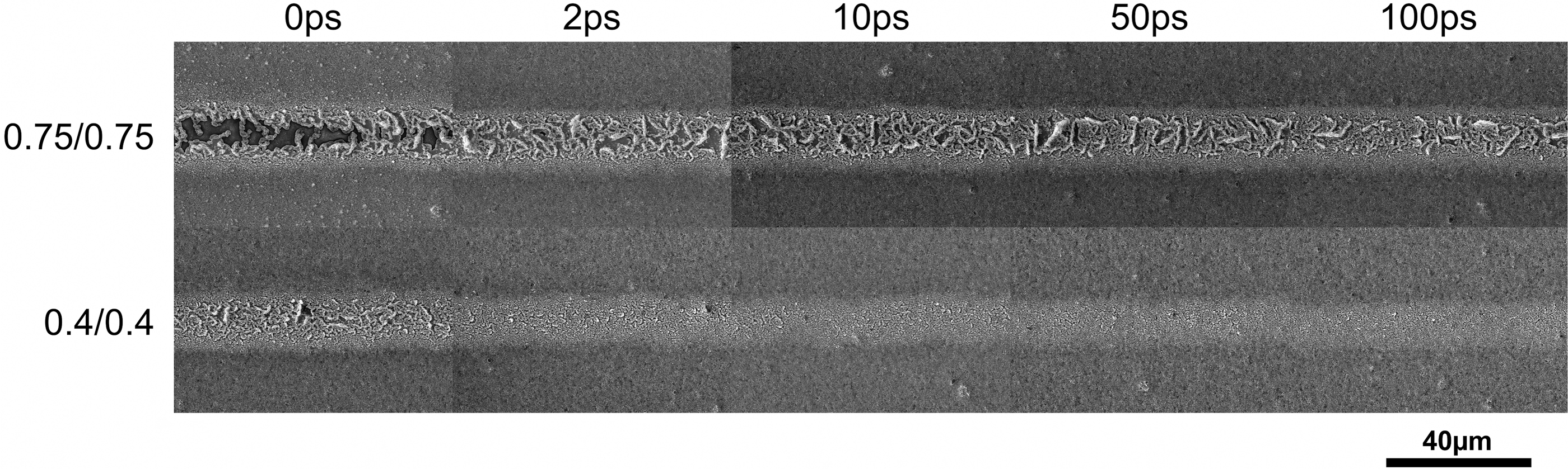
Plotted in Figure 3 are the scanning electron microscopy (SEM) images (FEI Quanta 650 ESEM) of spot sintering with double-pulse trains at various laser powers and different delay times. With laser powers of 1/1 and 0.75/0.75, Cu NPs are ablated across a large area, but only the particles near the edge of the laser spot are sintered. With zero-time delay (two pulses overlap in time), near the laser spot center, even the gold films underneath the powder are ablated. With increasing delay, the ablated areas shrink quickly, while the sintered area increases rapidly, and the gold films are preserved. Within the ablated region, gold film displays some color change that indicates melting, which spreads to the whole ablated region for 1/1, but only to partial of the ablated region for 0.75/0.75.

Top view SEM images of double-pulse train sintering of Cu NPs with respect to intensities and delay times. 1/1 means the individual fs-pulse has an average power of 1 mW. The last column presents cases with single fs-pulse with energy equal to an individual pulse in the double-pulse train, for example, a 1 mW single pulse for the row of 1/1.
When the delay time is longer than 50 ps, the ablated area does not show obvious change. The ablated area still remains even to a delay time of 1000 ps (Supplementary Data for results at more time delays). For 0.5/0.5, minimal ablation is observed after 10 ps. For 0.4/0.4, no ablation occurs after 2 ps. For 0.3/0.3, the energy is low enough that no ablation occurs even at zero-time delay.
For comparison, the last column of Figure 3 presents cases with a single-pulse train with laser power equal to the one pulse in the double-pulse train (e.g., 1 mW for 1/1). For cases of 1 mW and 0.75 mW, even the single-pulse cases still show a small area of ablation. With double-pulse train, the ablated regions are much larger than that with a single pulse. For these two cases, splitting the total energy to more pulses (e.g., 3 or 4) may further improve the efficiency of sintering. A single pulse of 0.5, 0.4, or 0.3 mW does not induce any ablation effect. For these three cases, double-pulse train sintering shows great advantage when proper delay time is chosen, such as larger sintering area, twice as much energy deposited, and no ablation.
Out of intuition, we might expect that when the delay time is long enough, the result with a double-pulse train would tend to become similar with the case of a single pulse. Our results suggest a different story. In the double-pulse train, the second pulse always sees the consequence left by the first pulse, and continues the work based on this consequence. When the separation of two pulses is shorter than the time required for electrons to become equilibrium with phonons, the second pulse starts its work in a high Te environment, and further increases the Te and hence the hot electron effects. The overall Te in the Cu NPs depends on the separation time of two pulses, as shown by our simulations of TTM (Fig. 1b).
When the separation time is much longer than the e-ph coupling time, the second pulse mainly sees the effect of the first pulse left on the lattice. When first pulse already melts a substantial amount of Cu NPs and even ablates a small amount of them (e.g., 1 and 0.75 mW), the second pulse sees particles with much higher lattice temperature than room temperature, larger size, and wider size distribution than the unsintered ones. As a result, even at the longest time delay (1000 ps for our experiments), the effects with double-pulse trains are drastically different with those of single pulse. For both 1/1 and 0.75/0.75, at long delay times, the ablated area has irregular shapes, and is not concentrated around the center of the laser spot. This phenomenon suggests that the second pulse selectively ablates particles with certain shape/size.
We also want to point out that with single-pulse trains, successful sintering could be only realized with laser power of 0.3–0.6 mW; with double-pulse trains, successful sintering could be achieved from 0.3 to 1.3 or 1.4 mW. The laser power window for successful sintering is expanded to more than two times.
Sintered area
Figure 4a plots the change of sintered area with delay time, at various laser powers. The sintered area is defined as the region covered with sintered particles subtracting the ablated region (if there is any). Both the areas of sintered particles and the ablation are estimated from the SEM images. One example shown is the inset of Figure 4a for case 0.5/0.5, the region of sintered particles (A) is circled with red line and the region of ablation (B) is circled with blue line. The sintered area (S) equals to area A−area B. For the cases of 1/1, 0.75/0.75, and 0.5/0.5, the smallest sintered area occurs at 0 ps delay time due to strong ablation. With longer delay time, the sintered area increases rapidly for cases 1/1 and 0.75/0.75 and peaks at around 100 ps.

Sintered areas with respect to
For case 0.5/0.5, the sintered area increases slowly with delay time and stabilizes at around 50 ps. The overall trend of sintered area with delay time is determined by two factors: region of sintered particles (A) that decreases with delay time and ablation (B) that also decreases with delay time. For the cases of 1/1 and 0.75/0.75 where strong ablation occurs, initially the decreasing of region B is much faster than that of region A, resulting in a fast increase of sintered area. After 100 ps, slight decrease of sintered area is observed because the ablation region (B) stops changing while the region of sintered particles (A) still shrinks slowly with delay time. For 0.5/0.5, the ablation region (B) shrinks dramatically from 0 to 2 ps, and then slowly after that and disappears after 10 ps, resulting in a moderately increasing and then stabilized sintered area.
The sintered area starts to decrease again after 200 ps. For 0.4/0.4, where slight ablation was observed only at 0 and 2 ps, the sintered area starts to drop after 6 ps. For 0.3/0.3, where no ablation occurs even at 0 ps, the sintered area decreases monotonically with delay time. The blue triangles shown in Figure 4a are the sintered areas with single-pulse trains. Without strong ablation (e.g., 0.4/0.4 and 0.3/0.3), double-pulse sintering produces substantially larger sintered area. With strong ablation (e.g., 1/1), the sintered area at 0 ps is close to that with single-pulse train.
Figure 4b plots the sintered area against laser power at various time delays. Overall, the sintered area decreases with lowering laser power, despite strong ablations occurring at high powers. It is worth to note that for the cases without strong ablations (0.5/0.5, 0.4/0.4, and 0.3/0.3 at 10, 20, and 50 ps), the sintered area increases linearly with laser power, as marked with the red dashed lines. The linear trends confirm the validity of our simple approach to estimate the sintered area.
Average particle size
Figure 5a shows the average size of sintered particles against delay time at different laser powers. The average size is estimated with sintered area (S)/number of particles in the sintered area. The number of the sintered particles are counted by linked clusters after the images are thresholded. (Please see Supplementary Data for details.) For the cases with ablation (0.5/0.5, 0.75/0.75, and 1/1), the average size does not show obvious dependence with delay time, except that a small peak shows up around 100 ps. With longer delay time, the region of sintered particles (area A) becomes smaller, which reduces the number of particles counted. At the same time, the ablation area shrinks quickly, which increases the number of particles counted. These two competing factors result in a weak dependence of average size on delay time.

Average sizes of sintered particles with respect to
For 0.4/0.4 and 0.3/0.3, where there is no strong ablation, the average size decreases along delay time. The blue triangles mark the average particle size with single pulse, which is significantly smaller than the double-pulse case at all laser power levels. Figure 5b shows that the average size decreases with laser power regardless of the delay time.
SEM images of line sintering
Figure 6 shows the results of line sintering for cases 0.75/0.75 and 0.4/0.4. These two powers are chosen to represent cases with and without strong ablation. The scanning speed is set as 4.5 μm/s without a mechanical shutter. A slow scanning speed allows more particles to be sintered compared with spot sintering cases because the exposure time per unit area is longer. For 0.75/0.75 with 0 ps delay time, the sintered surface is very rough, and there are many clustered chunks of sintered particles surrounding the ablation regions. By increasing the delay time, the sintered surface turns smoother. At 100 ps delay time, only some small clusters of sintered particles are visible.
Line sintering with a scanning speed of 4.5 μm/s with respect to laser power and delay time.
For the 0.4/0.4 case, weak ablation is only observed at 0 ps delay time, and the sintered lines are pretty smooth with longer delay time. For the spot sintering of 0.4/0.4 intensity setup with 2 ps delay time from Figure 3, there is still a tiny, ablated region, but there is no ablated region in line sintering with the same intensity and delay time setup. It may be because the exposure time of the incident laser for the line sintering is much longer than that of spot sintering. These line sintering results also suggested that the ablation not only causes removal of NPs from powder bed, but also leaves large roughness in the sintered NPs. Hence controlling the ablation will not only achieve successful sintering but also promote the surface smoothness.
HAZ in the substrate
Figure 7a plots the side-view SEM images of line-sintering for cases 0.75/0.75 and 0.4/0.4. First, we want to point out that the side-view image is averaged over the whole focal depth of SEM, not a single position along the depth. The black layer represents the gold thin film, above which is the Cu NPs and below which is the glass substrate. The discontinuity shown in the black layer indicates ablation/melting of gold layer itself.
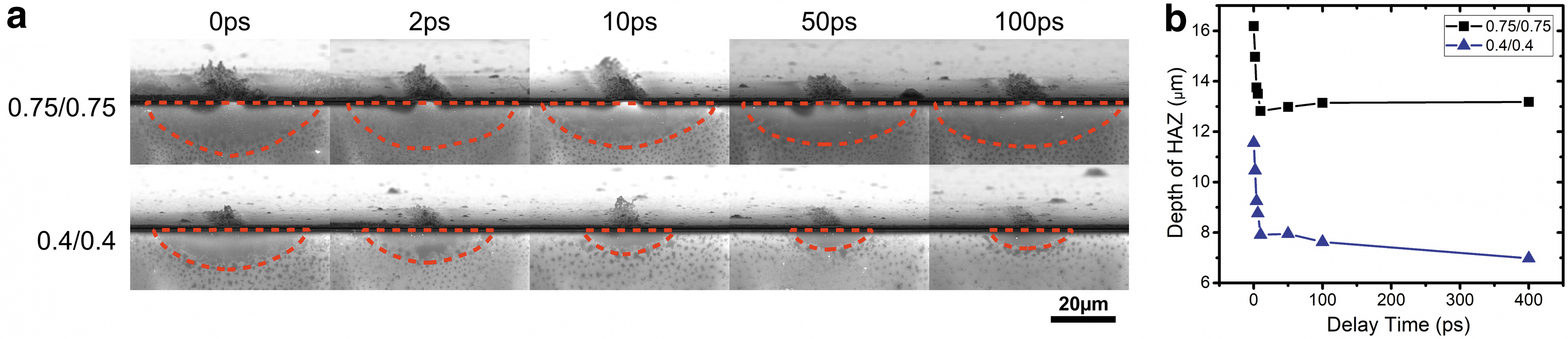
The change of the height of sintered clusters with delay time can be clearly revealed from these side-view images. For the 0.75/0.75 case, even though the height of sintered clusters decreases with delay time, it is always above the unsintered film even at 100 ps. For 0.4/0.4 case, nothing shows up above the unsintered film after 10 ps.
In the glass substrate, right underneath the sintered region, there is color change from light gray to dark gray. The color change is related with the HAZ in glass substrate, which is circled by red dashed lines with hemispherical shape. We use the radius of the hemispherical shape (
For the 0.75/0.75 case,
When sintering with CW or ns lasers, HAZ is mainly caused by heat diffusion. With fs laser, hot electrons play an important role on HAZ. After being generated in the Cu NPs, hot electrons can diffuse into the powder bed, across the gold film and scatter at the surface of glass substrate with the phonons in the substrate. How fast and how deep the heat could inject into the substrate depend on the velocity of hot electrons, which is proportional to the square root of hot electron temperature. Therefore, controlling the hot electron temperature has a direct impact on the depth of HAZ in the substrate.
X-ray photoelectron spectroscopy analysis for oxidation
Figure 8 shows the results of both regular X-ray photoelectron spectroscopy (XPS) (Cu 2p) and the Auger (Cu LMM) Spectra. (See Supplementary Data for details of XPS measurements). All spectra show only the Cu(I) peaks that correspond to Cu2O, with no trace of Cu(II) peaks related with CuO. Cu2O is present whenever the NPs are exposed to air, so initially all the particles are oxidized to Cu2O at the surface. By comparing the XPS data of unsintered with sintered Cu NPs, we noticed that the peaks do not show obvious shift for all the delay times, which indicates that the chemical states do not change. Our conclusion is that sintering with our fs laser pulse does not generate CuO, regardless of the delay time. This observation is rather a surprise because oxidation is very common during laser sintering, especially at such small scale.
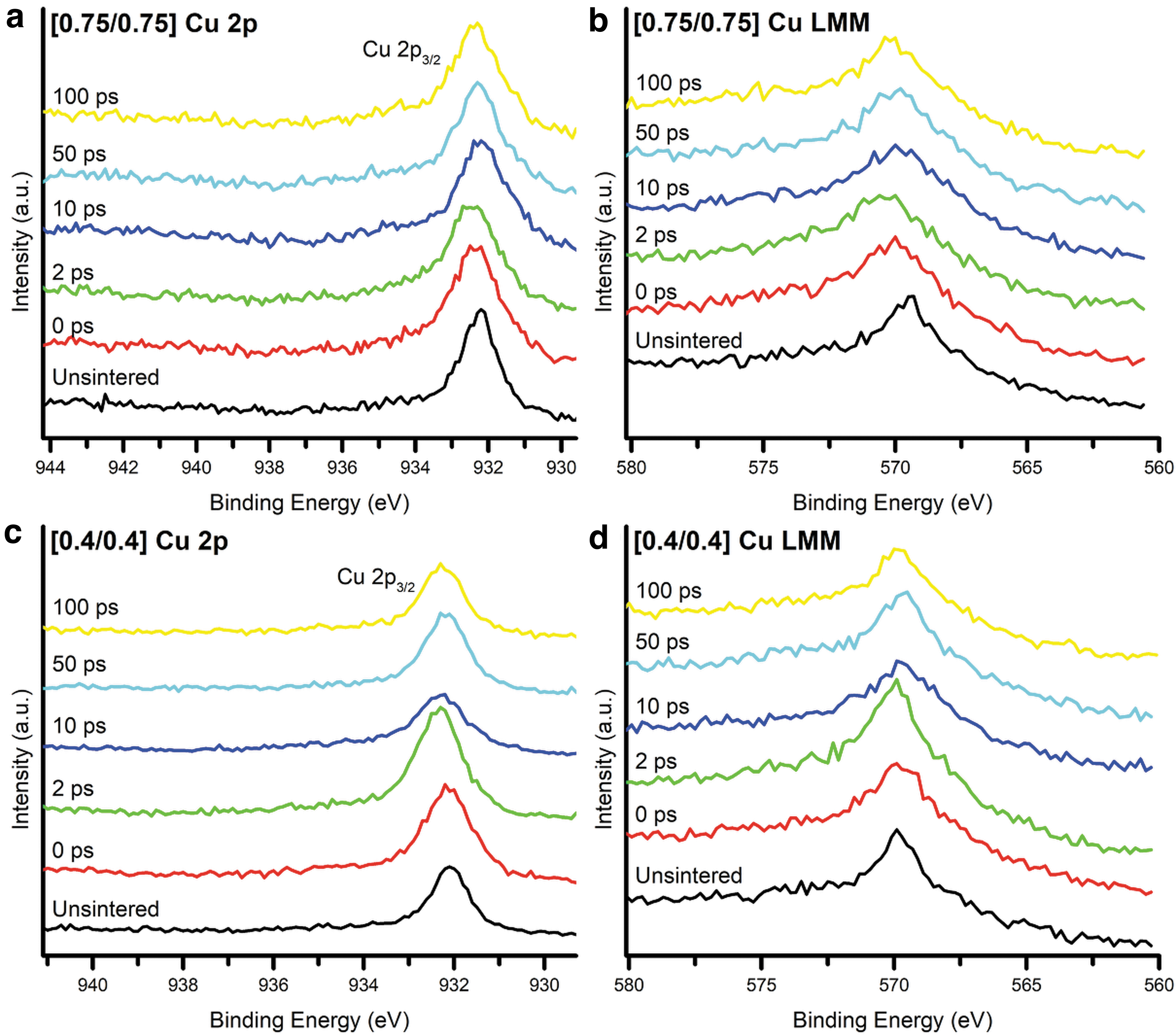
XPS spectra of
In literature, He et al reported fs laser induced oxidation in Cu thin film. The laser used in their experiment is 1040 nm with 50 MHz repetition rate and 100 nJ pulse energy. 38 Multiring-like structure was observed, where CuO is generated near the center region (higher fluence) and Cu2O in the outer region (lower fluence). For comparison, they also performed experiment with a single fs laser pulse (from a low-repetition rate laser) with pulse energy of 10 μJ. Instead of oxidation, they observed craters surrounded with Cu NPs. Gong et al conducted thermal oxidation experiments on Cu film and found that Cu2O is formed when T < 300°C, while CuO develops when T > 300°C. 39
Based on these previous experiments, formation of CuO requires temperature to be maintained higher than 300°C for extended period of time that there is enough time for the oxygen to diffuse into the material. Our laser condition (5 kHz, 800 nm, ∼100 nJ pulse energy) can induce high temperature only for very short period of time (up to tens of ns). Hence, there is not enough time to form CuO in our experiments.
It is worth to notice that there is obvious broadening of XPS peaks comparing the sintered cases with the unsintered one. This broadening could be caused by inhomogeneity induced by sintering, 40 for example, different phases of Cu2O. 38
Conclusion
In summary, a double-pulse sintering strategy with double-pulse train of fs laser is proposed for reducing the electron temperature in metal NPs and hence eliminating the ablation caused by hot electron effects. Power-dependent sintering experiments with double-pulse trains are conducted in Cu NPs film. It is clearly shown that the ablation region shrinks significantly when the two fs pulses are delayed by proper time. At some laser powers, the ablation is completely eliminated. The successful sintering laser power range is extended by about two times. Another important effect of sintering with double-pulse train is the reduction of HAZ, up to 66% by area. Even though in this report, we only demonstrated the effectiveness of using two fs pulses, the same idea can be further developed to three or more pulses, which would be explored in future work.
Footnotes
Authors' Contributions
J.P.: investigation, experimental setup, validation, data curation, resources, and writing—original draft. Z.Y.: experimental setup. H.C.: XPS experiment. Y.W.: conceptualization, methodology, writing—review and editing, supervision, project administration, and funding acquisition.
Author Disclosure Statement
No competing financial interests exist.
Funding Information
This work was supported by National Science Foundation under grant CBET-1934357.
References
Supplementary Material
Please find the following supplemental material available below.
For Open Access articles published under a Creative Commons License, all supplemental material carries the same license as the article it is associated with.
For non-Open Access articles published, all supplemental material carries a non-exclusive license, and permission requests for re-use of supplemental material or any part of supplemental material shall be sent directly to the copyright owner as specified in the copyright notice associated with the article.