



Abstract
An investigation on enhanced surface passivation in the existing industrial process line of large area n-type silicon (Si) Passivated Emitter Rear Totally diffused (n- PERT) solar cell has been performed. The Rapid Thermal Process (RTP) optimization for 20 min is conducted in the temperature range of 500–900°C and device evaluation is carried out with respect to regularly processed n-PERT solar cell. The impact of pre-metallization annealing is studied with the support of cell parameters like shunt resistance, reverse saturation current density determined from current-voltage measurements. The enhanced surface passivation via hydrogenation from silicon nitride (SiNx) layer during annealing is established with the help of external quantum efficiency, spectral response measurements and Fourier transform infrared spectroscopy analysis. The addition of optimized annealing resulted in improvement by 550% (from 38 to 247 µs), 7.73% (from 630.7 to 678.8 mV) and 84.77% (from 223.3 to 34 cm/s) in effective minority carrier lifetime, implied open circuit voltage and surface recombination velocity respectively. Finally, RTP technique for optimized process line has been successfully incorporated in industrial high-volume batch of 140898 CZ n-type Si wafers, which predicts conceptual validation of the study in mass scale production line with an increment in average efficiency of the device by 0.35%.
Keywords
Introduction
The generation capacity of renewable energy across the world is increased by 176 Gigawatt (GW) in 2019. The wind, solar energy based renewable sources have contributed 90% of the capacity of total renewable energy added in this year and in these technologies solar energy alone added 98 GW. Thus, solar energy-based technologies have outperformed all rest other renewable technologies and has seen tremendous expansion globally in installation from few Megawatt (MW) to close to 100 GW. 1 Amongst these technologies, the photovoltaic (PV) industry continued to face relentless competition due to pressure of lower prices and higher solar module power output cost
In recent years, to address the scarcity of energy, the PV industry has grown rapidly with various associated technologies in this direction. Out of all technologies, the conventional p-type crystalline silicon (c-Si) cells lead the whole PV market. 2 This type of standard c-Si solar cell has n-type and p-type semiconducting layer as emitter and base respectively along with full aluminium back surface field. The texturization and doping followed by silicon nitride (SiNx) passivation layer on the front and then screen-printed silver paste metallization can produce c-Si solar cell efficiency up to ∼ 20%.3,4 But these p-type c-Si solar cells have high temperature coefficient, serious light-induced degradation5,6 and light and elevated temperature induced degradation, which shrink the performance of Si solar cell and drop in electricity power generation during its field application in solar panels. If c-Si solar cell device architecture is based on n-type wafer then the fabricated device has no detrimental effect of light-induced degradation and elevated temperature induced degradation. These advantageous features in n-type c-Si solar cells are ascribed to the absence of boron doping in base layer of solar cell. So far, commonly reported n-type Si wafer-based technologies are heterojunction with intrinsic thin layer, 7 interdigitated back contact,8,9 tunnel oxide passivated contact 10 and passivated emitter rear totally diffused (PERT) in laboratory scale. 11 To address challenges in efficiency enhancement of p-type c-Si solar cells, the continuous developments such as surface passivation,12,13 laser opening 14 and aluminium screen-printed local back surface field 15 are needed. Based on the surface passivation idea, a variety of solar cell architecture like passivated emitter rear locally diffused (PERL), passivated emitter rear contact (PERC) and PERT devices are recommended for the fabrication of high efficiency solar cells. 16 The PERT technology is at large most suitable technology for mass production at present amongst all and this mono or polycrystalline Si wafer based solar cell technologies offer relatively simple involved processes and moderate cost In addition to it, the bifacial structure of PERT can take benefit of the diffuse reflection light on the rear, which further escalates the power generation output. Amongst all, n-type c-Si wafer-based technology i.e., n-PERT provides advantages such as superior tolerance to general impurities (e.g. iron),17,18 high bulk lifetime and near zero light-induced degradation. So, as a result, n-type crystalline-Si based PERT structure Si solar cell provides advantage of high working efficiency of solar cell which involves process optimization in a cost-effective manner.
Currently surface passivation of defects is critical in Si wafer-based PERT solar cell technologies to evaluate device performance. In these technologies, in-situ grown boron silicate glass during boron diffusion on Si surfaces forms unsatisfied silicon bonds. These unsatisfied bonds show energy states lies within the silicon material band gap and so generate several recombination centers. These recombination centers or defect levels hinder the charge carrier movement and so reduces minority carrier lifetime significantly. 19 Though thermal oxidation step drastically reduces these trap centers compared to the bare Si surface but still the processing steps for device formation introduce defects in such manner that these bonds still remain unsatisfied significantly after oxidation. Further rise in recombination centers in Si after oxidation can be attributed to subsequent processing step such as firing steps required for the formation of the screen-printed front and back contacts. Many research groups have reported efficiency enhancement through surface passivation in Si solar cell due to the thermal annealing incorporation at different processing stages such as before SiNx layer, after SiNx layer or during metallization with annealing temperature range (500–1000°C) which depends on type of doping processes (ion implantation or diffusion) and type of Si wafer (n or p-type) used in PERT device architecture.20–22 These studies show that thermal annealing after boron and phosphorous doping in front and rear surface of bifacial solar cell at higher temperature range (950–1050°C) has resulted into appreciable enhancement in absolute efficiency of ∼0.5%. The high temperature (>1000°C) annealing is prerequisite to fully activate ion implanted boron atoms at front surface for the increase in surface passivation. Recently, a research group reported pre-firing annealing (550–750°C) process prior to metallization in device fabrication line and found it to be promising for efficiency enhancement of the device. This device comprised phosphorous diffused doping on both sides of p-type multicrystalline Si (mc-Si) wafer. 23 The reported work signifies the importance of pre-firing annealing (temperature range 550–750°C) in mc-Si wafer based bifacial p-PERT- solar cell for short duration (3 s to 6 min) and observed efficiency enhancement via hydrogenated SiNx layer into Si which is leading to the minimization of the dangling bonds in emitter and bulk surface. Thus, minimum annealing temperature (>500°C) is required to activate unsatisfied bonds in Si surface for bonds saturation. Herein, an investigation on optimization of this pre-firing named as pre-metallization annealing is performed for enhancing surface passivation in the n-type monocrystalline Si wafer-based PERT i.e. n-PERT solar cell production line. This device comprises boron and phosphorous diffusion in front and rear surface and RTP is carried out in the temperature range of 500–900°C for 20 min. Our previous study already depicts efficiency improvement due to pre-metallization thermal annealing in the temperature range of 500–900°C for 20 min in these n-PERT solar cells via I-V curve measurements. But it was limited to variation in solar cell output parameters such as open circuit voltage, short circuit current and fill factor of the devices with respect to annealing temperature only. 24 Now, we have extended this work and additionally supported this study with Fourier transform infrared spectroscopy, scanning electron microscope, external quantum efficiency, reflectance, electroluminescence and minority carrier lifetime measurements of fabricated devices, for optimization of device annealing temperature. Moreover, after optimizing this process line for a device, it is applied on a mass scale production line of total 140,898 n-type monocrystalline Si wafers, which confirm yield and reliability of this technology in the existing production line. All the related device parameters are analyzed in view of that of variation in RTP annealing temperature. The fabricated n-PERT solar cell device surface morphologies were analysed by Scanning Electron Microscope (SEM) (Make: Zeiss - EVO-18). Class AAA tester system for I-V measurement by cetisPV was employed for electrical evaluation of all n-PERT devices under AM 1.5G spectrum with solar irradiance of 1000 W/m2 at device temperature of 25 °C. The minority carrier lifetime analysis was conducted using Sinton WCT-120 instrument in generalized analysis mode with minority carrier density injection of 1015 cm−3. Benthem PVE300 was used for External Quantum Efficiency measurements in the wavelength region of 300–1200 nm. In order to confirm hydrogenation effect in silicon-hydrogen bonding, Fourier transform infrared measurements was conducted using Perkin Elmer with ATR technique in the wave number range of 1000–3500 cm−1. The Electroluminescence testing of fabricated n-PERT solar cell was performed using halm EL tester having short wavelength infrared high resolution CMOS camera.
Experimental section
The n-type monocrystalline pseudosqaure CZ Si (100) wafers of area 157.35 × 157.35 mm2 with a specific resistivity of 2.1 Ohm-cm and thickness of 170 µm were employed in the fabrication of n-PERT solar cell. Initially, we removed the saw damage and conducted wafer cleaning process. Then, the micro texturing process was performed to form micro-pyramidal structure on wafer surface by wet chemical etching in alkaline solution at 80°C for 25 min. This was followed phosphorous diffusion using phosphorous oxychloride (POCl3) as dopant source for the formation of rear emitter of n-type. This diffusion process was conducted till rear emitter achieves its sheet resistance to 110 Ω/sq. which was measured by in house set up for four-point probe method. After rear emitter formation, antireflection-coating (ARC) via SiNx deposition was carried out by plasma-enhanced chemical vapour deposition (PECVD) in Centrotherm cPLASMA tube furnace at temperature of 430°C. Post rear ARC with n-type diffused wafer is followed by front surface wet texturization using industrial type alkaline solution processed line comprising alkaline solution with industrial chemical additives to perform optimum etching of Si surface with suitable ambient conditions. This front textured Si wafer is subjected in Centrotherm diffusion furnace for boron diffusion via Boron tribromide (BBr3) as a source dopant. The diffusion is performed to achieve front emitter of the cell with a sheet resistance of approximately 80 Ω/sq. This Boron diffusion of Si wafer confirms design of front emitter in the device which was followed with edge isolation using HF/HNO3/H2O chemicals. So formed front emitter is then deposited with SiNx layer using PECVD tools at a deposition temperature of 430°C. All these processed Si wafers were also incorporated with the optimum use of phosphosilicate and borosilate glass which results into electron-selective (thermal-SiOx/C-Si(n+)) and hole selective (thermal-SiOx/C-Si(p+)) passivated contacts onto both sides of wafer with passivated (SiNx) layer on front and rear emitter sides.
Finally, prior to metallization at the end of device fabrication process line, RTP annealing with N2 ambient in the temperature range of 500 to 900°C was performed with an augmentation of 100°C for around 20 min in industrial tube furnace. The additional annealing effects due to RTP were analyzed at each temperature and optimized for enhancing solar cell efficiency. All these processed Si wafers with different RTP treatments were subjected to same screen-printed metallization on both side of the devices for electrical contacts (front and back) and then followed with co-firing at a peak temperature of 835°C using an industrial infrared firing furnace (Centrotherm). The same metallization conditions for each device were implemented in as fabricated n-PERT solar cells (without and with annealing at different RTP temperatures). Since, optimization of RTP annealing was performed just before the metallization therefore herein it is termed as pre-metallization annealing also. The process flow chart of n-PERT device fabrication for without and with annealing are shown in Figure 1((a) and (b)). A typical adopted device architecture of n-type Si wafer-based PERT solar cell technology is shown in Figure 2.
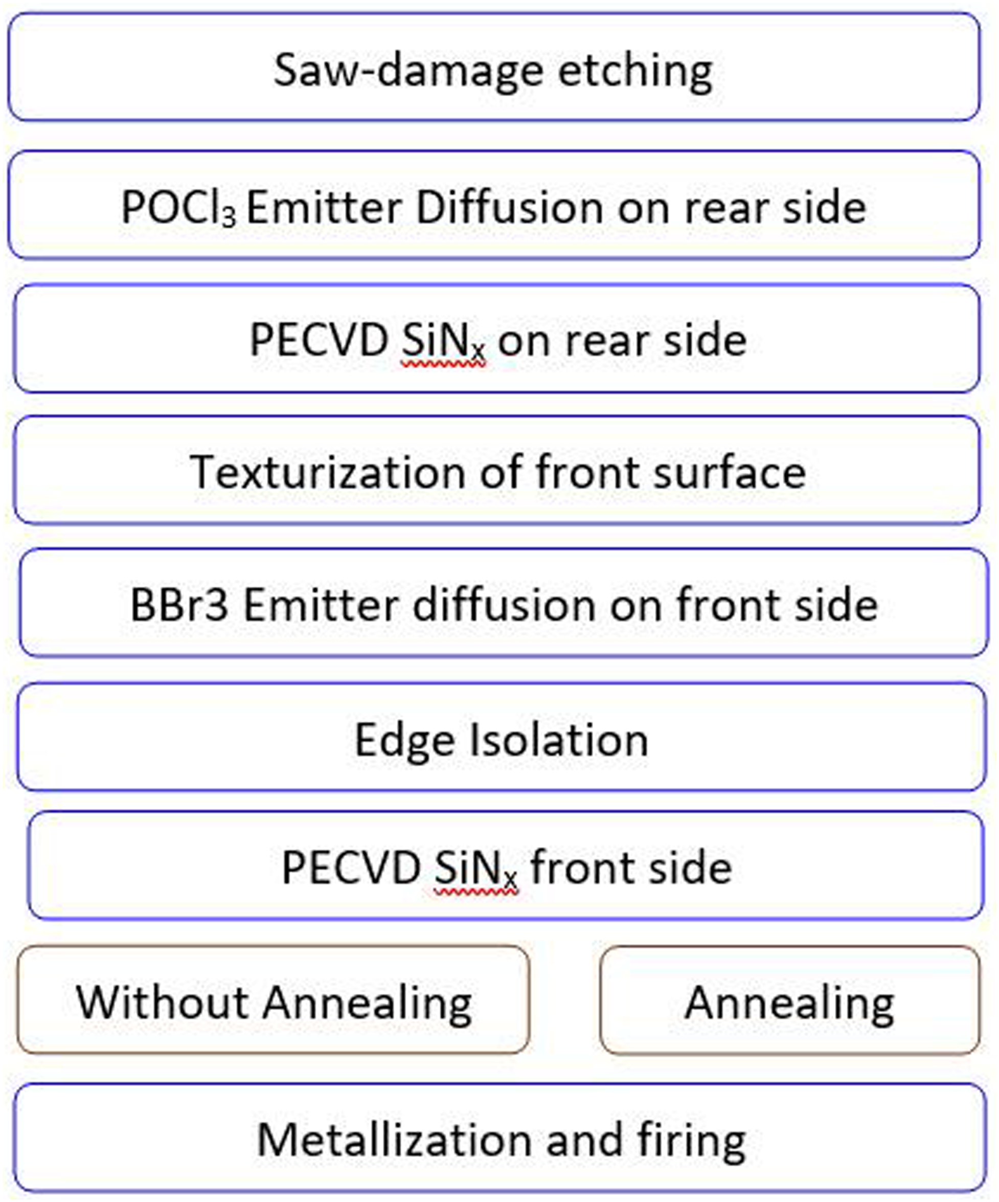
Process flow chart of n- PERT solar cell (a) without and (b) with RTP annealing.
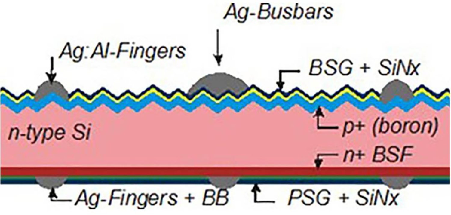
Device architecture of n-PERT solar cell.
Surface analysis
The surface morphology of as fabricated n-PERT cell is being analyzed by Scanning Electron
Microscope. The front surface of the device is shown in Figure 3(a) and shows formation of pyramids type structure after alkaline texturization of the surface. These pyramid's dimension is found to be lying in the range of 2–3 µm and is confirmed the same from Figure 3(b) in tilted view. The screen-printed metallic finger on top of textured surface is shown in Figure 3(c), which confirms standard alignment of metallic fingers along with binding on textured Si surface. The metallic particles in these screen-printed fingers with higher magnification are also shown in Figure 3(d) and confirm that after fast firing it has formed better inter-particle bonding.

SEM images of (a) textured surface (b) textured surface-tilted view (c) metallic finger on textured surface (d) metallic particles of fingers in a typical n-PERT solar cell.
The reflectance measurement of front surface of fabricated n-PERT solar cell for without annealing and with optimized annealing of 700°C in the wavelength region 300–1200 nm are shown in Figure 4. The observed reflectance shows no appreciable change in reflectance due to annealing and both reflectance spectrum are matching with typical antireflection (SiNx) coated and textured silicon surface.
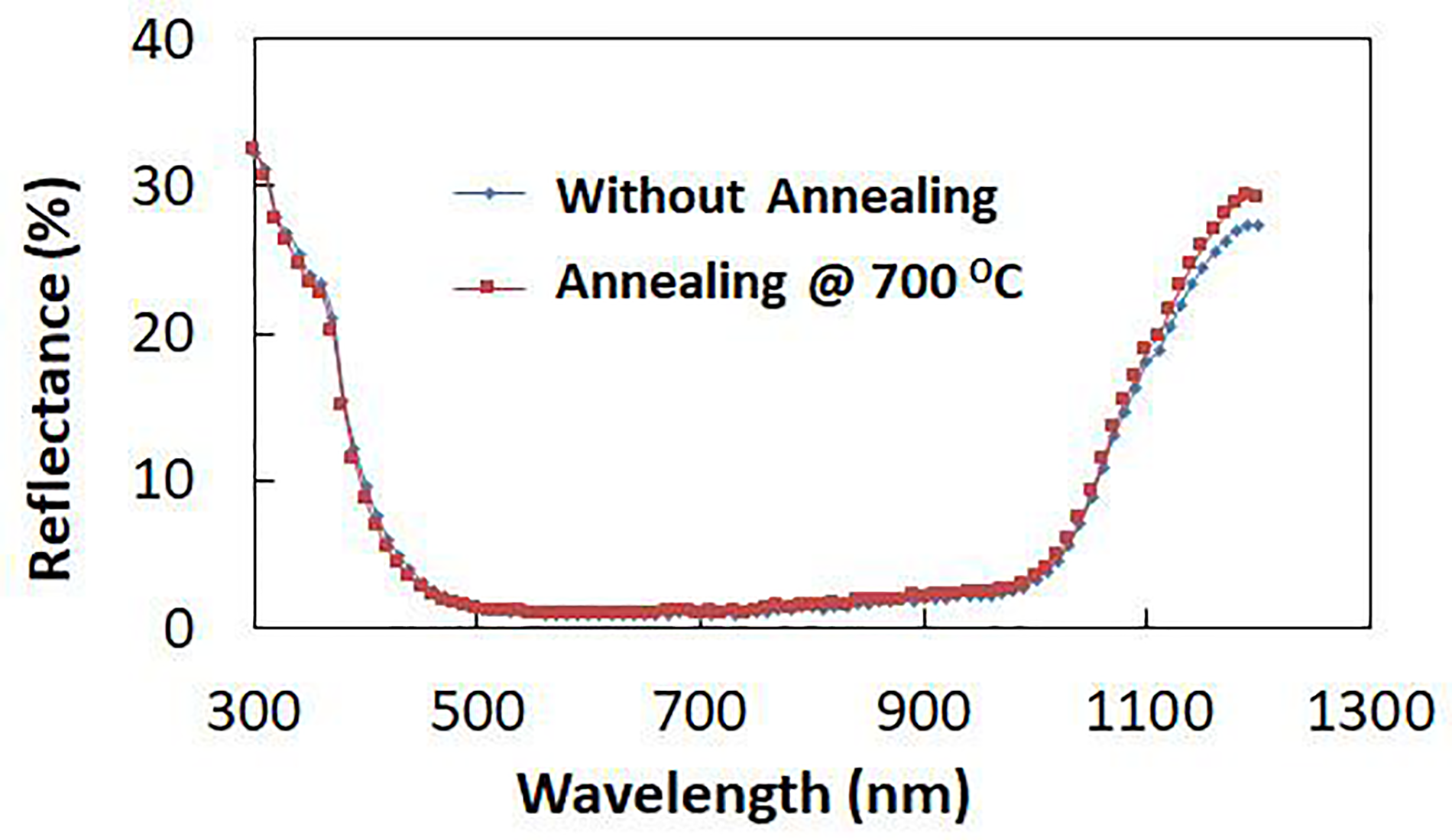
Reflectance spectra of without and with annealed n-PERT solar cell.
External quantum efficiency analysis
Figure 5 shows the external quantum efficiency response of the n-PERT c-Si solar cell at different pre-metallization annealing temperatures with the wavelength region of 300–1200 nm. The reference (without annealing) sample has an average external quantum efficiency (EQE) of 77%, while cells treated with annealing temperature at 500, 600, 700, 800 and 900°C have average EQEs of 81.3%, 82.5%, 82.8%, 82.3% and 77.3% respectively, over the entire wavelength range 300–1200 nm. The solar cell treated with annealing temperature 700°C has the highest improvement in the short wavelength region (300–400 nm) while relatively lesser appreciation is observed in visible (400–700 nm) and near infrared (700–1200 nm) wavelength region for optimized pre-metallized annealing at 700°C with respect to untreated device. The overall major improvement in external quantum efficiency is observed in wavelength range of 320–580 nm for annealed devices. Furthermore, the cell treated with annealing temperature at 900°C shows the decrease in EQE compared with other annealed samples and reference (without annealing) sample, indicating that the photo response is decreased with the increase in the annealing temperature beyond 700°C. The average weighted EQE in UV (300–370 nm) and visible (400–700 nm) regions for n-PERT Si solar cell are shown in Figure 6. The highest weighted EQE % in UV region for annealed sample at optimized temperature of 700°C is 66.27% in comparison to that of 62.5% for untreated sample. The average weighted EQE increase in short wavelength region clearly indicates improvement in front surface passivation or decrease in front surface recombination in the device. 25 The least weighted EQE in UV region for sample annealed at 900°C confirms significant front surface degradation at higher annealing temperature with respect to controlled sample, which can be ascribed to effusion of hydrogen at higher annealing and therefore reduction in passivation of the dangling bonds in bulk of Si wafer occurs.

EQE measurement of without and with annealed n-PERT solar cell.

Weighted EQE in UV region for without and with annealed n-PERT solar cell.
Figure 7 shows the spectral response of the six different n-PERT Si solar cells in the wavelength region of 300–1300 nm. The average weighted spectral response value of without annealed device is 0.1702 A/W-nm while device treated at 500, 600, 700, 800 and 900°C are 0.1710, 0.1759, 0.1808, 0.1758 and 0.1222 A/W-nm respectively. The improved front surface passivation and so reduced recombination can be confirmed via increase in spectral response in short wavelength region. 26 The cell treated with annealing temperature at 700°C for 20 min clearly indicate highest spectral response value compared with the other annealed cells as well as reference (without annealed) cells. The measurement shows maximum increase in average weighted spectral response value for device annealed at 700°C which is an enhancement of 6.2% with respect to without treated device in the short wavelength region of 300–370 nm. This spectral response of the device in short wavelength region is degraded with increase of annealing temperature beyond 700°C and the decrease in response is found to be significantly to 28.2% with respect to untreated device at 900°C. This least spectral response in short wavelength region confirms front surface deterioration of n-PERT solar cell due to higher temperature annealing i.e. at >700°C.
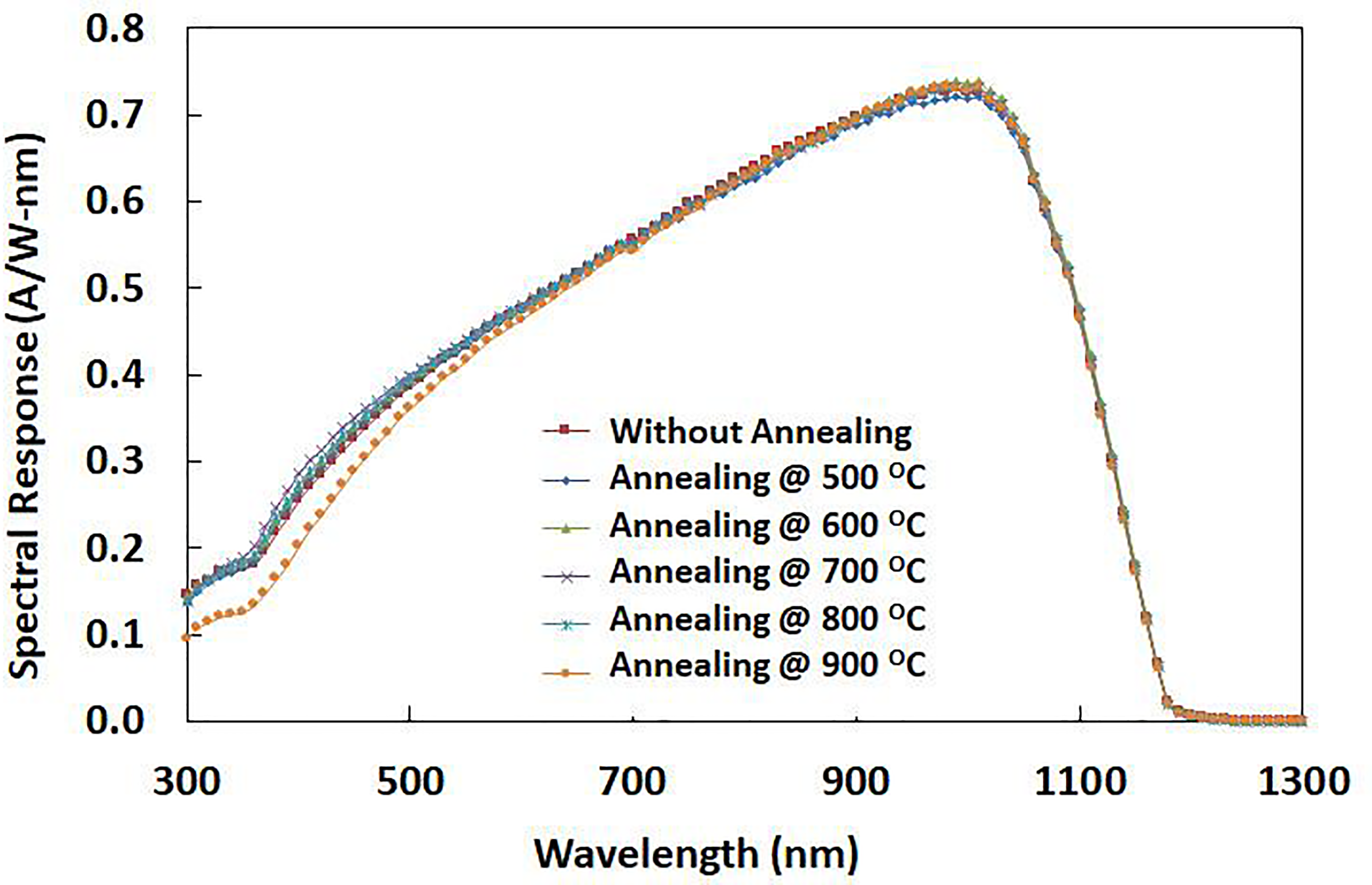
Spectral response measurement for without and with annealed n-PERT solar cell.
The shunt resistance is caused by defects on Si surface and in the bulk as well as from leakage currents or alternating current path across the edge of the cell. This parameter shows a parallel high-conducting path across the p-n junction which causes a reduction in both amount of current through the junction and voltage. The reduction in current and voltage decreases the efficiency of the cells by increasing the leakage current (measured by reverse saturation current (Io)) that lowers the maximum output power (Pm), the open-circuit voltage (Voc). The RSH of a solar cell is determined using illuminated I-V characteristics of the cell extend from the fourth to the third quadrant while Io can be evaluated by dark I-V measurement.
27
Thus, Rsh and Io are crucial cell parameters to its performance during its field applications in the PV panel. The I-V equation for a solar cell under illumination in the presence of a shunt resistance is given by
28

The study of measured I-V curves were already reported in our previous communication, which is showing efficiency enhancement of n-PERT solar cell from 20.72% for without annealed to 21.03% for optimized annealed sample at 700°C. Accordingly, improvement in other output cell parameters such as, open-circuit voltage, short-circuit current and fill-factor (FF) variation with annealing temperature were observed. To extend this analysis further, herein shunt resistance (Rsh) and reverse saturation current density (Jo) variation extracted from I-V are presented in the Figure 8, which is showing variation of this parasitic resistance with rapid thermal annealing effect on the as-fabricated n-PERT solar cells. The Figure 8 clearly shows enhancement in Rsh due to annealing till optimized annealing at 700°C is achieved and then reduction is observed with increase in annealing temperature till 900°C. The exactly opposite behavior in reverse saturation current density with respect to shunt resistance is observed with increase in RTP temperature. The enhancement in shunt resistance from 2560 to 3931 Ω due to annealing till 700°C and reduction in reverse saturation current density from 771 fA/cm2 for without annealed sample to 139 fA/cm2 confirms reduction in crystalline defects, which helps in reducing recombination in the device. The reduction in recombination of carriers occurs due to increased hydrogen passivation via annealing, which assures better performance of the device during its field application.

Shunt resistance and saturation current density variation for without and with annealed n-PERT solar cell.
Thus, optimized annealing at 700°C confirms achievement of minimum leakage current for this device. Hence, n-PERT solar cell annealed at 700°C confirms less crystalline defect along with least leakage current makes device to operate with higher working efficiency in field applications. The extracted data from I-V measurement are further summarized in Table 1.
Summary of extracted data from I-V measurement for without and with annealed n- PERT solar cell.

The above I-V table shows the electrical parameters of n-PERT Si solar cell treated with different annealing temperature. While comparing the electrical parameters of cells without and with optimized annealing temperature, unable to see any difference in series resistance. Since this annealing is performed before metallization process, so different annealing temperatures will not have any impact on finger or bus bar resistances. There is a possibility for changes in series resistance only due to lower surface concentration at higher annealing temperatures due to further drive-in and will lead to higher contact resistance during contact formation. Above table shows higher series resistance at annealing temperature of 900°C followed by the degradation of fill factor.
The qualities of screen-printed metallization on as fabricated without and with annealed n-PERT solar cells are observed by EL image testing, as shown in Figure 9. The annealing treatment is not at all affecting the front surface metallization of n-PERT solar cells as shown in below EL images.

El images of without and with annealed n-PERT solar cells.
To investigate the passivation effect, lifetime measurement was conducted using WCT-120 photo-conductance in generalized mode for analysing cell performance under minority carrier density of 1015 cm−3. The measured effective lifetime for as-fabricated and rapid annealed n-PERT solar cell for without and with RTP annealing are shown in Figure 10. Figure clearly depicts significant improvement in the effective minority carrier lifetime with the increase in RTP annealing temperature till 700°C. The variations in effective minority carrier lifetime for n-PERT solar cell due to RTP annealing at 500, 600, 700, 800 and 900°C are 56, 173, 247, 219 and 72 μs, respectively, while without annealed device show lifetime to be merely 38 μs. Thus, n-PERT solar cell shows significant enhancement in effective minority carrier lifetime from 38 μs to 247 μs for annealed sample at 700°C, which is almost 6.5 fold higher than controlled sample. A decrease in the improvement with respect to controlled device was observed after increase in pre-metallization annealing temperature beyond 700°C. A significant drop of ∼71% is observed for RTP annealed 900°C device with respect to the optimized one. This confirms that excessive RTP annealing at higher temperature is detrimental to minority carrier lifetime. Thus, lifetime evolution strongly depends upon the pre-metallization annealing temperature and on optimal RTP temperature in the device can help in improving minority carrier lifetime and confirm passivation of crystalline defects. The surface recombination velocity (SRV) is one of the most important determining parameters of surface passivation in a solar cell. Therefore, surface recombination velocity of the charge carriers is calculated for each annealed sample and compared it with controlled device. Herein, the as procured Si wafers features such as resistivity and thickness are used as 2.1 ohm-cm and 170 μm, respectively. The bulk lifetime (

The measured effective minority carrier lifetime (
The minority carrier injection in photoconductivity analysis also helps in evaluating the important device passivation parameter such as implied Voc. The measured implied Voc for all respective n-PERT devices are shown in Figure 11. This device performance parameter found to show variations according to the RTP annealing temperature profile and well-tuned and analogous to other surface passivation parameters such as
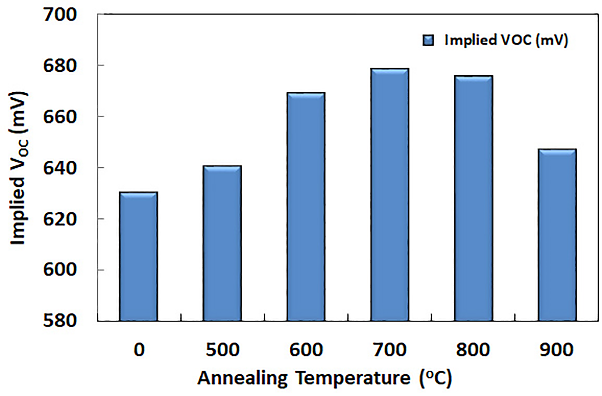
Implied VOC for without and with annealed n-PERT solar cells.
The oxide passivation step due to RTP annealing after phosphorus diffusion in the process line of device fabrication (Figure 1) causes further improvement in charge carrier lifetime values which leads to the reduction in surface recombination velocities and hence surface passivation via hydrogenated SiNx layer occurs in the device.
Herein, atomic hydrogen diffuses from SiNx layer through oxide layer and passivates dangling bonds. The mobility of bound hydrogen is critical as it is expected that the degree of passivation (as measured in minority carrier lifetime) depends on the amount of hydrogen released from the SiNx film into the bulk of wafer. 32 The release of hydrogen from SiNx film is increased with RTP annealing temperature in the range of 500 to 700°C, which can be depicted via reduced hydrogen presence. This reduction of hydrogen leads to the removal of contaminants and structural defects from the bulk of silicon after cleaning and saw damage removal. The RTP annealing beyond 700°C results into out diffusion of hydrogen from Si-SiNx interface and can be confirmed via increased silicon-hydrogen bonding at surface. This enhanced effusion of hydrogen from hydrogenated SiNx results into reduction in surface passivation in the device.33,34 Defect hydrogenation in Si is studied using attenuated total reflectance Fourier Transform Infrared spectroscopy. Figure 12 provides the Fourier Transform Infrared Transmission spectra for three hydrogenated SiNx layers grown with RTP treated at 700 and 900°C temperature (sample B and C) and without annealed (sample A) n-PERT solar cell. In order to understand surface passivation through hydrogenation from SiNx layer, most prominent feature is hydrogen bond associated with silicon and nitrogen in transmission spectrum. The transmission bands observed at around 2160 cm−1 and 3340 cm−1 are assigned to Si-H and N-H stretches. 35 The majority of H is bound to Si for without annealed n-PERT sample and measured transmission band is found to be with 0.94 change for sample A. If this device is RTP annealed at 700°C, a reduction in transmission band of Si-H is observed and change in transmission is found to be 0.78 as depicted in inset image of the Figure 12. This confirms reduction of hydrogen in silicon with increase of RTP annealing temperature till 700°C. This reduction in hydrogen is consumed in reducing defects of silicon and helping in enhancing bulk passivation of device. The outward diffusion of hydrogen from Si-SiNx interface is confirmed from increased transmission band intensity (from 0.94 to 0.99) of Si-H bonding for n-PERT solar cell annealed at 900°C, which is shown as sample C in inset image of Figure 12. Thus, RTP annealing study in the temperature range of 500–900°C of n-PERT solar cell reveals that the associated mechanism involves hydrogen bond dissociation followed by molecular in and out diffusion depending on variation of RTP temperature which can lead to increment or decrement in surface passivation parameters measured by variations in charge carrier lifetime, implied Voc, SRV values. All these passivation parameters are responding in similar manner to RTP heat treatment in n-PERT solar cell and maximum passivation is achieved for device annealed at 700°C.

The Fourier transform infrared measurement for without and with annealed n-PERT solar cell.
The improved performance of large size n-PERT solar cell device is clearly showing enhancement of 0.33% in its absolute efficiency due to pre-metallization RTP annealing at 700°C. The optimized RTP annealing for improved device efficiency with n-PERT architecture (Figure 2) has been implemented in the batch process line. The device level study is further confirmed in mass production line with volume of 1,40,898 CZ Si wafers. Out of total CZ Si wafers, 61000 wafers were processed for device fabrication in absence of annealing and rest of wafers (79,898) were processed with RTP annealing at optimized temperature of 700°C in the n-PERT solar cell production line. The histogram represents efficiency distribution for without annealed and with annealed n-PERT Si solar cell in production line as depicted in Figure 13. The figure clearly shows percentage of cells at different efficiencies segregated within the band range of + 0.1% tolerance, i.e., all the n-PERT solar cells having efficiencies in the range of 21.00–21.10% will be notified as an average efficiency bin-of 21%. So, the histogram figure clearly shows that the optimized annealing temperature at 700°C treated cells depict highest efficiency compared to the without annealed device. The average efficiency of fabricated n-PERT devices at batch level for without and with optimized annealing are found to be 20.62 and 20.97%, respectively.

Batch wise solar cell efficiency for without and with annealed n-PERT solar cell.
Thus, successful integration of RTP annealing in existing process line of a commercial large size CZ-Si wafers for n-PERT solar cell device fabrication is established in a large volume production line. An average efficiency of 20.97% was demonstrated over a large production batch with average absolute efficiency improvement of 0.35% due to optimized RTP annealing.
In this work, we demonstrate the potential of incorporating optimized thermal heat treatment via RTP annealing for enhancing n-PERT solar cell performance with the support of I-V, minority carrier lifetime, external quantum efficiency and spectral response measurements. Herein, pre-metallization annealing in n-PERT process line is performed in the temperatures range of 500- 900°C with an interval of 100°C. The measured I-V curves indicate enhancement in shunt resistance and reduction in reverse saturation current density with optimized RTP annealing (for 20 min) at 700°C. The SEM measurements confirm typical pyramid's height in the range of 2–3 µm after texturization of Si surface. The External Quantum Efficiency measurement shows highest UV response in the short wavelength region (300–400 nm) and shows improvement of ∼6.5% due to optimized RTP annealing at 700°C. The spectral response and external quantum efficiency measurements show better UV response in n-PERT solar cell and so validate front surface passivation in the device. The hydrogen diffusion and effusion in the solar cell due to RTP annealing is confirmed from Fourier Transform Infrared analysis via decrement and increment in transmission band intensity of silicon-hydrogen bonding. The solar cell surface passivation signature parameters such as effective minority carrier lifetime(
Footnotes
Declaration of conflicting interests
The author(s) declared no potential conflicts of interest with respect to the research, authorship, and/or publication of this article.
Funding
The author(s) received no financial support for the research, authorship, and/or publication of this article.
