
Abstract
In the inductive wireless power transmission (WPT) designs of consumer electronics and implantable devices, the printed planar coil in standard manufacture is commonly used. Layout optimization of the coils is one of the important ways to make the power transmission system more efficient. Varying the trace width and turn-to-turn spacing together for the coils is proposed to optimize the maximum achievable power transfer efficiency (𝜂max). An accurate analytical model for the printed square coils is also established as well to speed up the design process. By virtue of this model, an optimal scaling factor of the trace width and the optimal frequency can be quickly estimated. The proposed model is validated by both the simulations (ANSYS HFSS) and experiments. A WPT link of two planar coils with size of 50 mm × 50 mm × 1 mm, operating at 23 MHz, is optimized by using this methodology. After optimization, the measured 𝜂max of the WPT system is increased from 22.60% to 32.74% at a 100-mm transmission distance.
Introduction
Wireless power transmission (WPT) technology has the advantage of no connecting wire between the transmitting (Tx) and receiving (Rx) sides when transferring the power, similar to the popular behavior of wireless signal transmission. WPT technology has found its application in many fields like industries (e.g., electrical vehicles and robots [1,2]), domestic and consumer electronics (e.g., televisions and smart phones [3,4]), and implantable devices (e.g., neural interfaces [5,6]). Inductively coupled WPT is commonly used in these applications where the power is transferred from the Tx coils to the Rx coils through the magnetic fields [7].
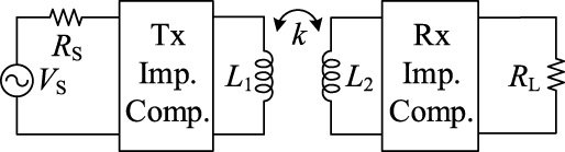
A diagram of two-coil inductively coupled WPT system.
A typical circuit diagram of two-coil inductively coupled WPT system is shown in Fig. 1, where V S and R S are the power source and its output impedance, respectively, R L is the equivalent load. L 1 and L 2 represent the Tx and Rx coils with the coupling coefficient k. The power transfer efficiency (PTE) of the WPT system is an important parameter which has been the optimization objective in many previous designs. Two impedance matching circuits are respectively inserted in the Tx and Rx sides to optimize the PTE, as shown in Fig. 1.
Different types of coils can be used for WPT. Although the three-dimension coils (e.g., solenoidal coils) have more optimization space than planar coils, they occupy more volume than planar coils. Planar printed coils, which can be realized on printed circuit boards (PCBs), thin flexible substrates (e.g., polyimide), Si substrate, etc., are suitable for industrial and commercial applications by virtue of their merits such as compact size, standardized fabrication, and good uniformity. Herein, we focus on optimization for the planar printed coils from the aspect of coil layout.
Traditionally, the planar printed coils are optimized by adjusting the geometries, such as trace width, number of turns, and height of substrate principally through iterative design [8]. The authors of [9,10] have proven that decreasing the trace width from outer turn to inner turn has the advantage of improving the quality factor of coils. This non-uniform trace width method is also combined with adjusting the inner diameter or the number of turns together [11]. In fact, the spacing between turns is also required to be optimized besides the trace width variation. In this paper, a new layout method of the planar printed coils is put forward. Different from previous work, the proposed layout method includes changes of both trace width and spacing, and thereby improves 𝜂max of the WPT system.
Although a full-wave electromagnetic field simulation tool can be used to find the optimal geometrical sizes, it is usually very time-consuming, that is because multiple coil parameters need to be optimized. An accurate analytical model of inductance, parasitic resistance, and parasitic capacitance (i.e., RLC model) is required to accelerate the optimization process. There are models of printed planar coil in [8] and [10], but the model in [8] is inapplicable for coils with non-uniform trace width, while the model in [10] is not fully quantified.
The rest of this work is organized as follows. In Section 2, the principle of the new layout optimization method by varying width and spacing of traces together is presented. In Section 3, the analytical model of the printed planar coil with non-uniform width and spacing is established. In Section 4, a design example is presented to illustrate merits of the proposed method and analytical model by both simulations and experiments. Finally, the conclusions are drawn in Section 5.
The maximum achievable PTE (𝜂max) for the WPT system as shown in Fig. 1 can be realized by using appropriate impedance matching circuits [12],
In [10] and [11], layout optimization methods are focused on reducing the resistance loss of the coil to increase the quality factor while keeping the coupling coefficient k almost constant. Such resistance loss comes from two parts, i.e., the skin- and proximity-effects resistances (R SK and R PR, respectively) which will be modelled in the next section. Proximity-effect resistance, caused by the eddy currents generated under the magnetic fields produced by the currents in the adjacent turns. For a multi-turn coil, from the inner turn to the outer turn, the strength of the magnetic field normal to the trace surface decreases firstly and then increases gradually, and the position with the minimum magnetic field strength is actually close to the outer turn [13]. That is to say, the inner turns where exists higher magnetic field strength suffer more proximity-effect resistance loss than the outer turns if uniform trace width is used for coils. Accordingly, narrower trace widths for inner turns were designed to reduce R PR [10–12]. The narrower trace width reduces the area of the conductor exposed to the magnetic field and further reduces the eddy current and the corresponding R PR. Besides, increasing the spacing between turns which reduces the magnetic field strength suffers from the currents of adjacent turns, can also reduce R PR. Therefore, decreasing the trace width and increasing the trace spacing together will further reduce R PR. On the other hand, the skin-effect resistance is proportional to the trace width. Therefore, a suitable trace width and trace spacing are required to be optimized to decrease the sum of R SK and R PR, and therefore to increase Q and 𝜂max values.
Conventionally, squared and circular printed planar coils are used in the WPT systems. Here, without loss of generality, the squared coil is studied. A typical squared planar coil is shown in Fig. 2a, where the geometrical parameters d
out, w, and s are the length of the outermost turn, trace width and trace spacing, respectively. Figure 2b shows the proposed schematic of an N-turn squared planar coil. The turns of the coil are numbered form n = 1 to n = N, starting from the outermost turn. In our design, the optimization principle is expressed as
According to (2), the efficiency 𝜂max is related with k and Q. Compared with the coupling coefficient k, the quality factor Q is affected much more by the scaling factor 𝛼 if the sizes of the coils (d out) are not changed. By calculating Q and 𝜂max based on the analytical modelling in Section 3, an optimal coefficient 𝛼M and an optimal frequency f M corresponding to the maximum 𝜂max can be obtained.

The layout of coils. (a) Conventional square planar coil, (b) proposed schematic of N-turn square planar coil.
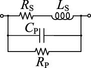
Lumped equivalent circuit model.
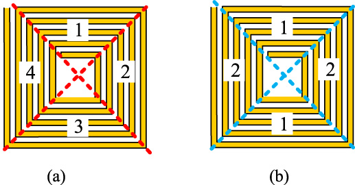
The coil is divided into identical parts to calculate M P and M N. (a) Dividing the coil into four parts. (b) Dividing the coil into two parts.
The lumped equivalent RLC circuit model of the planar coil is shown in Fig. 3. The analytical expressions for the inductance, the parasitic resistance, and the parasitic capacitance are established here.
The inductance calculation of multi-turn printed coils can use the results of the self-inductance of each turn and the mutual-inductance between different turns by using the partial inductance concept [14]. A commonly used and accurate formula from [15] is herein used. The total self-inductance of each turn is [15],
The mutual-inductance between the traces with the same (opposite) current direction is positive (negative) mutual-inductance. When calculating the positive mutual-inductance M
P, we divided the coil into four identical parts as shown in Fig. 4a. Then the expression is
Similarly, the negative mutual-inductance M
N is obtained by dividing the coil into two identical parts as shown in Fig. 4b,
The total inductance is the sum of the self- and mutual-inductances,
According to [16], the lumped self-capacitance of a coil can be modelled as the sum of the transmission line capacitance (C T) and external capacitance (C E), where C T represents the transmission line resonance property, and C E is the lumped capacitance between turns.
Many recent studies on the self-resonant frequency for multi-turn coils started from the transmission line resonance model [17–19]. Some results by using curve-fitting can be found in [17,18]. However, the impact from the substrate was not included in these models. According to the analysis in [19], if the transmission line is open, the transmission line length corresponds to one quarter of the fundamental resonant wavelength, i.e., l = 𝜆∕4. On the other hand, if the transmission line is shorten, the transmission line length corresponds to one half of the fundamental resonant wavelength, i.e., l = 𝜆∕2.
In practice, the coil is loaded by some circuits (e.g., rectifier circuits) in WPT applications or the measurement instrument (e.g., a vector network analyzer (VNA)). Due to the load effects, the self-resonant wavelength is usually between 2l and 4l. That is, the self-resonant frequency can be written as
With respect to C
E
, we got an approximation by computing the capacitances between the innermost turn and the outermost turn, which is similar to the method of approximating the lumped parasitic capacitance for a solenoid coil by calculating the capacitances of a pair of turns at both ends of this solenoid coil [16]. Then the expression is
The substrate on which the coil is printed commonly has different dielectric constant from the air, which leads to different dielectric environments above and under the conductor. Then the parasitic capacitance when considering the substrate, C
T(E), sub, can be separated into two parts, C
T(E)1 and C
T(E)2, corresponding to the capacitances above and under the conductor, respectively, as shown in Fig. 5a. The capacitance C
T(E)2 is determined by the thickness and the relative permittivity of the substrate. The whole environment under the conductor can be represented by using a uniform material with an effective relative permittivity (ϵr, eff), as shown in Fig. 5b. Based on the simulation data of printed coils under different thickness (t
sub) and relative permittivity of the substrate (ϵr) by using the HFSS tool (ANSYS, Canonsburg, PA), a curve-fitted formula of ϵr, eff is given as [21]
In the curve-fitting process, the accuracy for the case ϵr = 4.4 has high priority because FR4 is commonly used in WPT applications. Figure 5c shows a comparison between the model of ϵr, eff and the simulated results. A good agreement can be observed, especially when ϵr is less than 10. Then the parasitic capacitance C
T, sub and C
E, sub with substrate can be expressed as
In the WPT applications, the coil ends are usually loaded. A connecting line across the coil should be added between the inner and outer ends of a multi-turn coil. A stray capacitance C
OV exists between the overlap area of the connecting line and the coil. The overlapped capacitance C
OV is given as
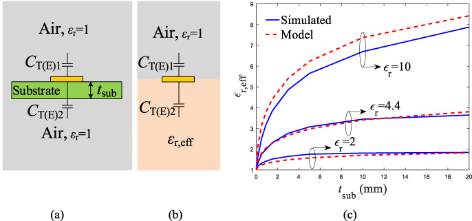
Modeling of the parasitic capacitance including the impact of substrate. (a) Parasitic capacitance is divided into two parts. (b) Environment under the conductor is equivalent to be an uniform material with an effective relative permittivity (ϵr,eff). (c) Comparison between the curve-fitted model of ϵr,eff and the simulated results from HFSS.
Finally, the total parasitic capacitance C
P can be obtained by adding up all such capacitance above,
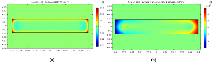
The skin-effect phenomenon is well-known for an isolated straight conductor under the AC condition, high frequency current will crowd on the surface of conductor when passing through it. Figure 6a shows a typical current distribution simulated by using COMSOL Multiphysics tool (Los Angeles, CA, 5.2), where the operating frequency is 100 MHz and the corresponding skin-depth, δ, is about 6.6 μm. For a multi-turn coil, the total skin-effect resistance, R
SK, is the sum of all the skin-effect resistances of the traces [9],
A typical high frequency current distribution on the surface of conductor. (a) Current distribution on a cross-section of a conductor because of skin-effect. (b) Current crowding effect on a cross-section of a conductor because of proximity-effect.
Besides the skin-effect, the proximity-effect is another important phenomenon leading to current crowding. When two parallel conductors carry AC currents, the magnetic field produced by one conductor induce eddy current in another conductor. Figure 6b shows a 2-D eddy current distribution on the cross-section of a conductor under a magnetic field normal to its surface, simulated in COMSOL Multiphysics, where the directions of the current in the left and right sides are opposite. Although the current crowding produced by the proximate effect is a well-known fact and the general mechanisms have been elucidated in some previously published articles, little information is available to quantitatively predict its magnitude without resorting to numerical simulations [22]. In previous studies, authors considered the eddy currents to be simply limited in the outer 1/4 of the trace width [13,23] or skin depth δ [24,25]. This simplification gives a rough approximation of resistance. Different from previous methods, inspired by the analytical calculation method of the proximity-effect resistance for a conductor with circular cross section [26], a similar method was proposed [27],
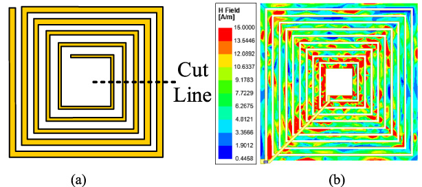
Cut line and simulated magnetic field related to magnetic field calculation. (a) Cut line at the middle of side. (b) Simulated magnetic field normal to the surface of planar coil.
Although the magnetic field normal to the surface of the nth turn, i.e., H
n
, can be calculated by summing all the magnetic field produced by the currents inside other turns, the magnetic field varies along the trace. In addition, this is a cumbersome work. An expression of H
n
is given in [11] by investigating the magnetic field distribution along the cut line as shown in Fig. 7a. However, simulation results show that the magnetic field at the corner is higher than the other positions as shown in Fig. 7b. Based on this phenomenon, we counted the ratio of the average magnetic field of the entire side of each turn to the magnetic field in the middle of each side, generating a compensation coefficient k
C = 1. 96. The revised expression of H
n
based on [13] is
Then a complete analytical model for R PR can be obtained by substituting (16) and (17) into (15).
The current crowding from the skin- and proximity-effects are combined altogether. Fortunately, because of the orthogonality of the skin- and proximity-effects [29], the skin-effect resistance (R
SK) and the proximity-effect resistance (R
PR) can be summed directly to obtain the total parasitic series resistance (R
S),
In addition to the substrate permittivity that introduces additional parasitic capacitance, the dielectric loss on the substrate also leads to additional power loss. That is, the relative permittivity of the substrate is actually a complex value, ϵr = ϵr
′
− jϵ”
r, where ϵr
′
and ϵ”
r are the real and imaginary parts of ϵr, respectively. Consequently, ϵr, eff is also a complex value and can be obtained by substituting complex ϵr into ((10)), i.e., ϵr, eff = ϵr, eff
′
− jϵ”
r, eff, where ϵr, eff
′
and ϵ”
r, eff are the real and imaginary parts of ϵr, eff, respectively. The power loss can be modeled as a resistance R
P (or a susceptance G
P) in parallel to the parasitic capacitance C
P, that is
From (3)–(19), the total impedance and quality factor of the coil can be deduced through R
S, L
S, C
P, and G
P,
When two squared planar printed coils are used as the coil link of the WPT, the coupling coefficient k is obtained by calculating Im(Z
11) and Im(Z
22) from (20) and the mutual inductance M between two coils [12],
The mutual inductance M from [30] is
Finally, we can get the achievable maximum PTE, 𝜂max, from ((1)).
In order to validate the layout optimization method based on analytical model, a set of multi-turn square coils are printed on 1-mm thickness FR4 substrates with various trace widths and spaces. All other geometrical parameters are fixed as follows: t = 35 μm, N = 6, w 1 = 2.8 mm, p = 3.3 mm, and d out = 50 mm. The optimization coefficient 𝛼 varies from 0.6 to 1 with a step 0.1. The coil with 𝛼 = 1 corresponds to the conventional coil with constant trace width. We put the above parameters into the formulas of the model to calculate Q and 𝜂max of coils through MATLAB (MathWorks, Natick, MA). The simulation is completed in HFSS. Figure 8 shows the measurement setup of quality factor where a coil is connected to a vector network analyzer (VNA, Ceyear 3656A) through a SMA connector.
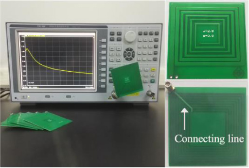
Measurement setup of quality factor for printed planar coils.
The parasitic parameters of the SMA are compensated by using the de-embedding method [6]. Y-parameters of the coils are measured by VNA. Y
full, Y
short, and Y
open, which correspond to the full, short, and open circuits, respectively. Finally, Z was calculated from (23) according to [6], consequently, Q can be obtained from (20).
Figure 9 shows comparisons among the calculated, simulated and measured quality factors at 1 ∼ 80 MHz. The simulated and measured results are basically agreed well with the calculated ones, sharing the same trend. The quality factor increases firstly and then decreases with the frequency increased, i.e., a maximum quality factor (i.e., Q M) exists for each case of scaling factor 𝛼. When 𝛼 = 0.8, Q M reaches maximum. The measured Q M is improved from 158 to 217 from 𝛼 = 1 to 𝛼 = 0.8. When the frequency approaches f FSR (about 80 MHz where Q closes to zero), there are some discrepancies between the results from measurements and those obtained by simulations and the proposed model. The reason is that measuring Z-parameters would not be accurate when the frequency is too close to the self-resonant frequency where the Z-impedance is close to infinite and thereby reducing the VNA excitation current and measurement accuracy [6].
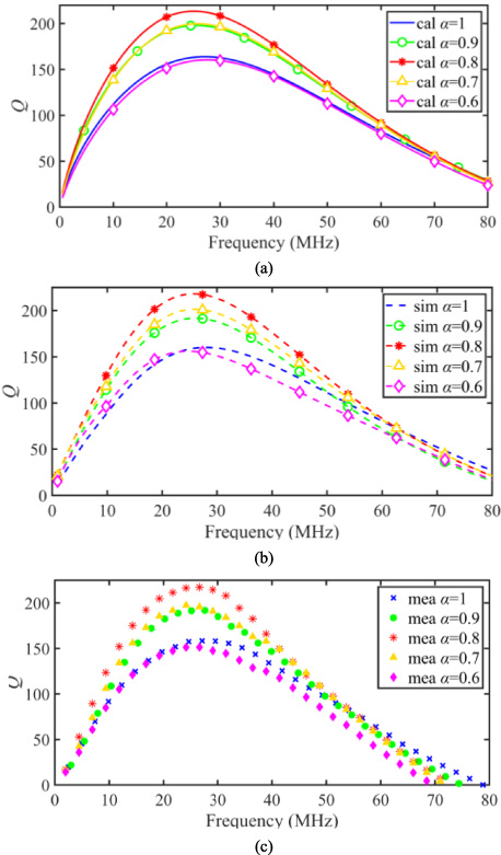
(a) Calculated, (b) simulated, and (c) measured results of the quality factors.
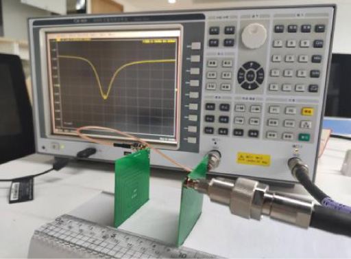
Measurement setup of WPT link by using printed planar coils.
A simple inductively coupled WPT link where both the Tx and Rx coils are the same is established to verify how the layout optimization affected the system power transmission efficiency. As shown in Fig. 10, the Tx and Rx coils which are placed face to face with 100-mm distance are connected to the VNA to obtain the Z parameters. The coupling coefficient can be obtained from (21) where the numerator part (i.e., ωM) actually is equal to Im(Z 21). And the values of 𝜂max can be obtained from (1).
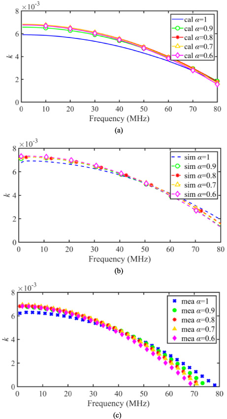
Comparisons among calculated, simulated and measured results of k between coils with different 𝛼.
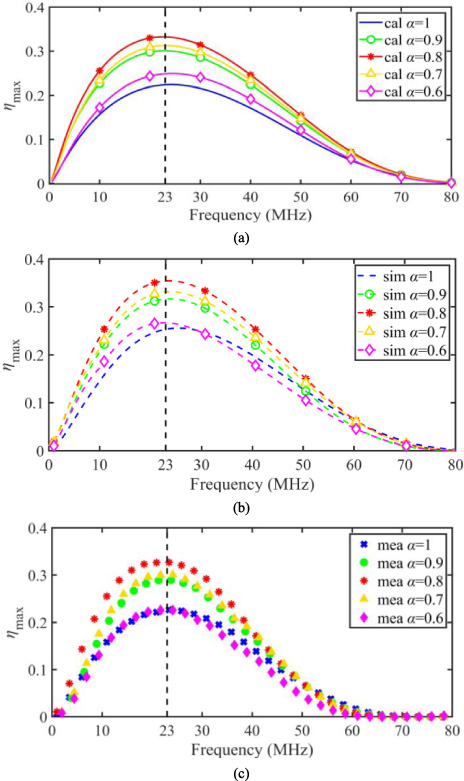
Comparisons among calculated, simulated and measured results of 𝜂max for different 𝛼.
Figures 11 and 12 compare k and 𝜂 max results of calculation, simulation, and measurement, respectively. The calculated results are consistent well with the simulated and measured results. As shown in Fig. 11, k varies slightly after layout optimization. It can be observed from Fig. 12 that a maximum power transfer efficiency 𝜂max exists for each case of scaling factor 𝛼. From Fig. 12a, the frequency corresponding to 𝜂max (i.e., the optimal frequency f M) is 23 MHz which is the same with the simulated and measured f M as shown in Figs 12b and 12c, respectively. This consistency further verifies the effectiveness of the analytical modelling of the coils and the WPT link. When designing a WPT system, f M is selected to be the operating frequency. For a specific application, if the operating frequency is limited to some specific region (e.g., 13.56 MHz), the designer should design the coil and adjust the compensation circuits to let the optimal frequency f M be inside the limited specific frequency region.
Calculated, simulated errors relative to and measured values, at 23 MHz
We also can find from Fig. 12 that the case with 𝛼 = 0.8 has the highest 𝜂max. Table 1 shows the calculated, simulated and measured Q, k, and 𝜂max at 23 MHz for different 𝛼. According to the measured results, the transmission efficiency at 23 MHz is improved from 22.60% for the traditional coils (𝛼 = 1) to 32.74% for the optimized coils (𝛼 = 0.8).
A new layout optimization method of planar square coil is proposed. The trace width from the outer to the inner turns declines in an equal proportion together with increasing the trace spacing. An accurate analytical RLC (resistance, inductance, and capacitance) model of the printed planar coil is developed. This model can accelerate the process of designing the wireless power transfer system and optimizing the power transfer efficiency. As a consequence, both the optimal scaling factor 𝛼 of the trace width and the optimal frequency can be quickly estimated without using the time-consuming electromagnetic field simulation tools. The proposed model has been validated by both simulations and experiments. The measured results show that the optimized power transfer efficiency of a WPT system is improved about 45%.
Footnotes
Acknowledgements
The authors gratefully acknowledge the support of the Zhejiang Provincial National Natural Science Foundation of China under Grant No. Z20F010015, the National Natural Science Foundation of China under Grant No. 61771175, and the Key Research Project of Wenzhou under Grand No. ZG2020016.