
Abstract
In this paper, a hill-climbing method is adopted to control the output of full bridge circuit to achieve desired constant voltage/current output. A novel technology also is presented to control the rising time of the DC converter output. The hardware implementation of this digital control is based on the Field Programmable Gate Array (FPGA) digital chip. The proposed hill-climbing control algorithm can automatically adjust the Pulse Width Modulation (PWM) control parameter to handle the DC converter output approaching desired one. High frequency power supply with DC switching circuit has been paying more attention to its small size, light weight, and small electromagnetic interference. Digital control has many different control modes than continuous circuit one, and digital control can be updated at any control mode, unlike continuous circuit design cannot be changed once it is completed. That is, the merit of digital control is flexible and programmable which is why the FPGA digital control used in this paper to control the DC switching circuit. We obtain the FPGA execution code by establishing its corresponding Matlab/Simulink simulation model. After meeting simulation test, the Matlab/Simulink model can be directly transformed into Hardware Description Language (HDL) code. This greatly saving the time of writing HDL code which often is a barrier to the electrical engineer. Finally, a high power, 7.2 KW, DC-DC converter experiment is presented to confirm the feasibility of the proposed control method and design procedure.
Keywords
Introduction
Recently, due to the increasing demand for high-power DC converters, many research reports have been proposed [1–6]. In the past, there were too many conductivity losses and overheating problems for a DC converter until that high frequency DC converter design with zero voltage switching [7–11] was presented but its output power was not high enough. So middle tap transformer and full-wave rectifier were presented to deal with the high power problem. Conventional controller’s implementation typically was analogical controllers [3, 8] or digital micro-controllers [12, 13]. The main drawback of analog control is that the control flexibility is poor and the control mode is completely limited to the ready-made component IC. Analog control often requires a larger volume of analog control circuit so that the corresponding circuit size and cost is relatively higher than digital one.
Because the dynamics of the DC converter with control are both high order and nonlinear where dominant poles have a time constant below 0.3 ms. If use the general micro-controller which is a serial implementation of program, it is difficult to achieve “against the instant impedance changes to increase the relatively stable output voltage” under the DC-DC converter closed-loop system. Speeding up the processing of data is the direction of solving above mentioned problem. And so, the FPGA chip with parallel computing was used to solve this problem recently.
Digitalization is the recent development trend resulting that FPGA digital control is more and more adopted by industry because its instruction operation can be done in hardware parallel mechanism. In each clock cycle, FPGA with a parallel mechanism can complete more operations than the digital signal processing (DSP). The FPGA hardware cost is cheaper than the DSP one. And FPGA design is more flexibility. So more FPGA controller papers are proposed to implement different control mode [14, 15] owing to its fast parallel data computing functions and low hardware cost. This is why we present a hill-climbing control law based on the FPGA chip to handle the full-bridge circuit to obtain constant voltage/current output with a desired rising time. The proposed hill-climbing control is different from the traditional PID control for that the proposed control can automatically adjust the control parameters to achieve desired system performance rather than manually adjusting parameter of PID. It is somewhat similar to the iteration method and is an effective control application. This paper also presents a novel method to control the system output approaching desired one at the desired set time because high power DC converter with slowly rising output control is an indispensable feature for the electroplating factory.
This paper is organized as follows: The configuration of the full-bridge DC converter is viewable in Section 2. Section 3 proposes the digital design algorithm with a rising time interval set for a DC converter. A given experiment shows the proposed controller’s feasibility in Section 4. Conclusions are summarized in Section 5.
Problem formulation and characteristics
A full-bridge type of DC-DC high power converter with a center-tapped transformer is shown in Fig. 1 [16, 17]. The parameters in Fig. 1 are described as follows: input DC voltage V in , output DC voltage V o , output current i o , Rs is a resistance referred as a shunt, purely for current measurement purpose. The coil ratio of the transformer primary and secondary side is N1: N2. Traditional phase-shifted PWM control to Fig. 1 is implemented by the hardware IC, not program writing IC, for completing constant voltage/current and zero voltage switching. The literature [18] has a detailed description of the above issues. The phase-shifted PWM technology in reference [18] can be plotted in Fig. 2 and summarized as belows:
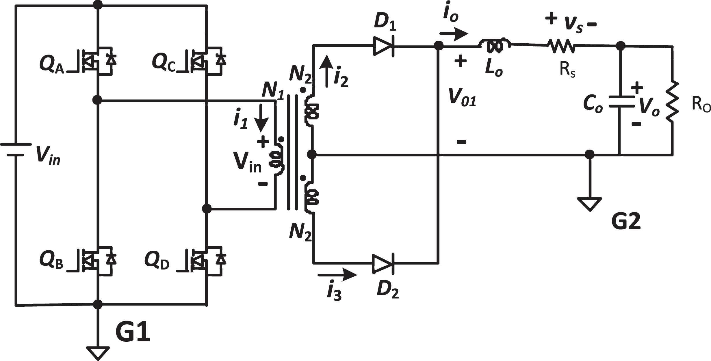
Full-bridge DC converter with center-tapped transformer.

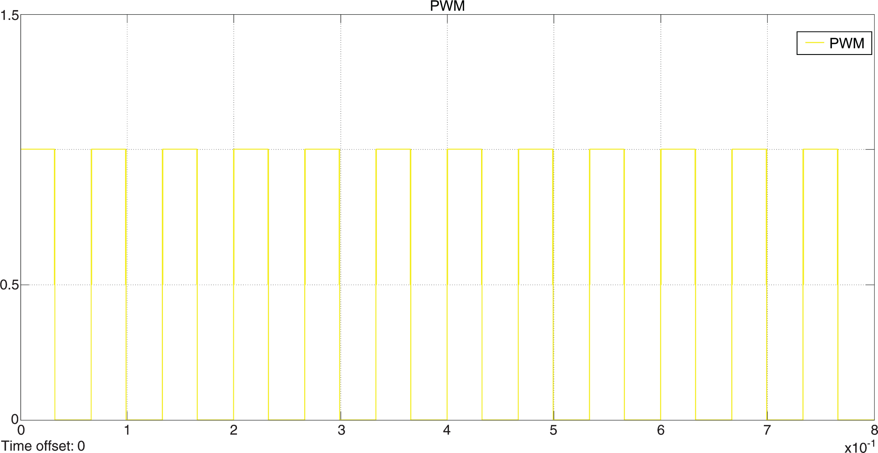
Phase-shifted PWM control.
(QA, QB) is a set of PWM square waves that are mutually opposite to each other with a fixed period T. The left and right edge time of QB high state waveform between the one of QA is Δt1 in Fig. 2. This Δt1 size affects the success or fail of zero voltage switching (soft switching).
(QC, QD) is a set of PWM square waves that are mutually opposite to each other with a fixed period T. Δt2 is the time that QC high state of the left and right edge distances the one of QD wave in Fig. 2. The suitable Δt2 is chosen, then the primary side of the transformer current will approach a constant value no jitter, that is called zero voltage switching (soft switching). That is, both Δt1 and Δt2 can affect soft switching ok or not.
The load output on the secondary side of the transformer depends on the length of the overlap Δt4 between QA and QD. The overlap between QB and QC is also set as Δt4. So, control the load output magnitude is equivalent to regulate the size Δt4.
Since QC and QD are a dependent PWM square wave to each other. When QC and QD are simultaneously delayed by Δt3 time, the Δt4 size, the overlap between QA and QD, will be changed simultaneously.
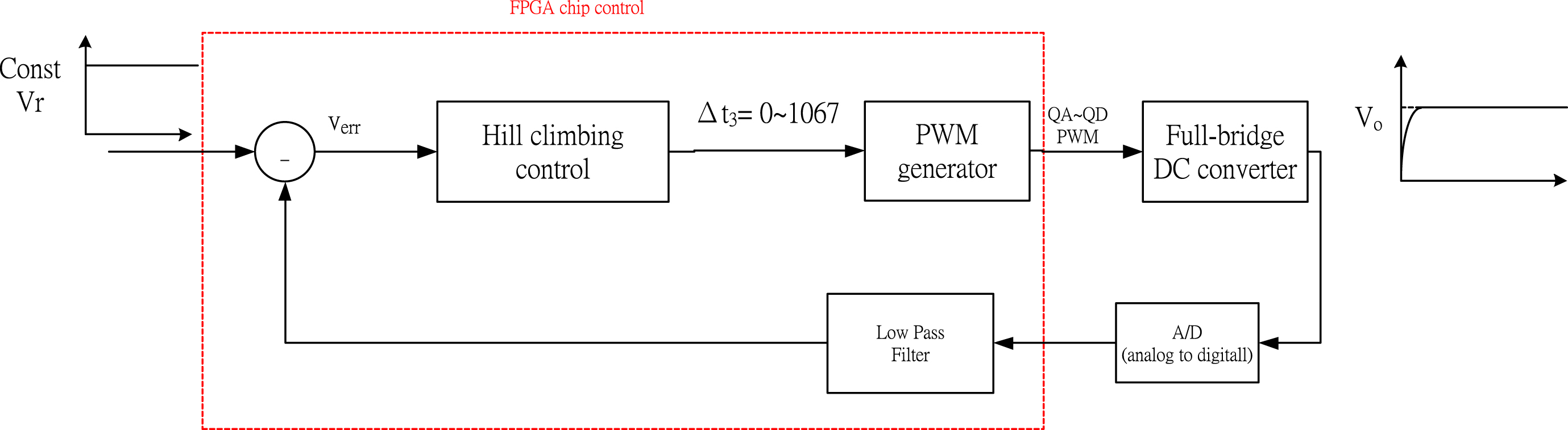
In view of the above issues, the larger the Δt3, the smaller the load voltage output obtains because the overlap amount Δt4 becomes smaller. Tunning Δt1 and Δt2 can get soft switching (zero voltage output). The entire system circuit among FPGA digital chip, analog circuit, and power switching components can be shown in Fig. 3.
The output voltage Vo1 on the secondary side of the transformer in Fig. 1 mixed with the control PWM Fig. 2 can be expressed as
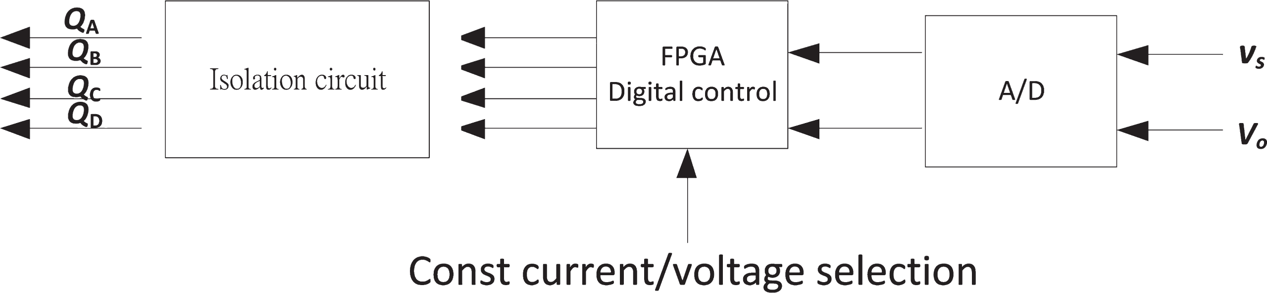
Relation between digital/analog circuit and power switching components QAQD.
where
After substituting (2) into (1), we have
By the Kirchhoff’s Voltage Law (KVL) law, the DC voltage on the secondary side of transformer can be written as
Substituting (3) into (4) obtains
where Δt3 is regarded as the control input to produce four QA ∼ QD PWMs, like Fig. 2, such that the system output V o approaches the desired constant voltage/current.
From (5) we know that the delay time Δt3 can influce output voltage V
o
and shunt voltage V
s
that is proportional to output current i
o
. Δt3 can be adjusted for producing suitable four PWMs, like Fig. 2, to handle output voltage V
o
to attain the desired one. This is regarded as a constant voltage control. On the other hand, if use Δt3 to control shunt voltage V
s
to obtain the desired current output i
o
then the control law is said constant current control. The magnitude of load voltage V
o
and current output i
o
shown in Fig. 1 is controlled by the delay time Δt3. That is, when the input Δt3 is small (large), then V
o
and i
o
are large (small). Based on the above discussion, this paper addresses the following issues: Constant voltage (CV) design V
o
≅ V
r
: Design a hill-climbing control in Fig. 7 to adjust the parameter Δt3 so that the load output voltage V
o
approaches the reference V
r
via the feedback signal V
o
; Constant current (CC) design CC or CV with slowly rising control: Let the output voltage or current reach the desired one at a time setting t
set
shown in Fig. 9.
The output port of the digital PWM controller is to produce four PWM square waves like Fig. 2. Then input to the power switching elements IGBTs. The following will describe the construction of the PWM square wave.
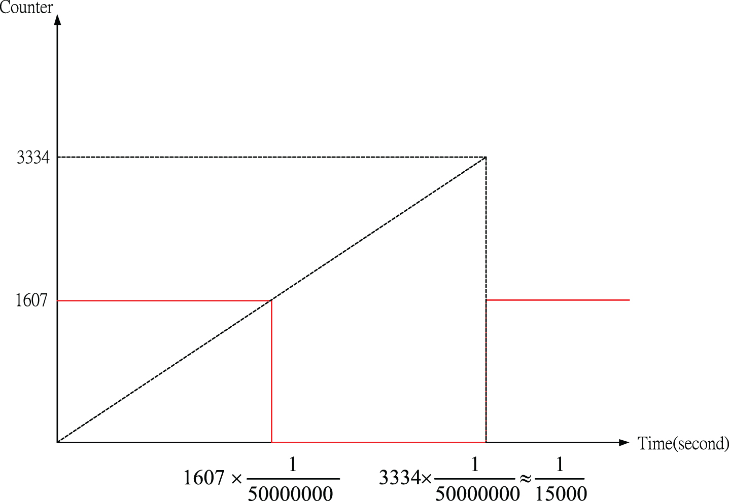
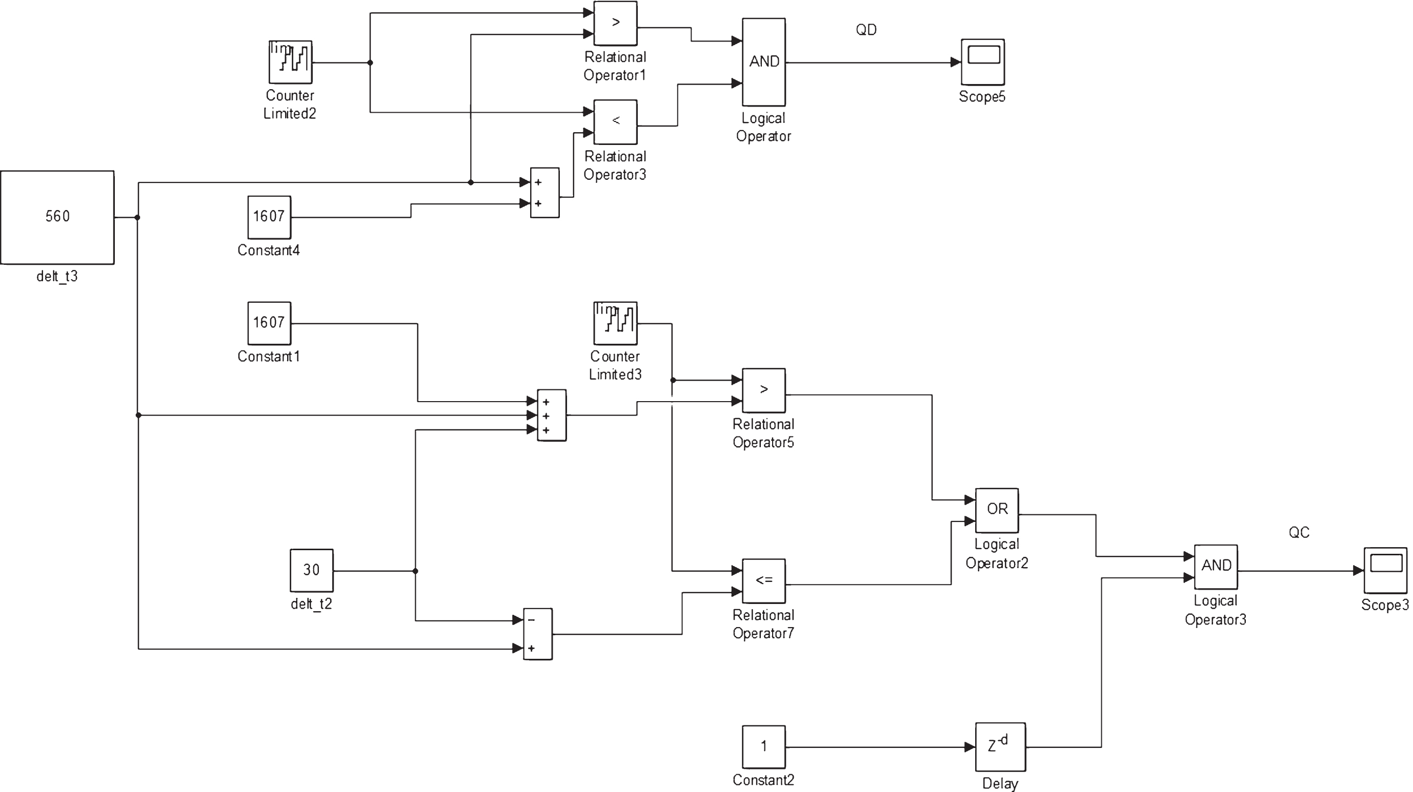
The QA square wave in Fig. 2 can be implemented by a counter and a comparator. Take an example to explain its design concept. In order to generate a 15KHz pulse of periodic wave, the counter with clock oscillation frequency 50 MHz counts up from 0 to 3334, repeatedly, and is compared with a constant 1607 to get a QA square wave. Mathematical express is shown as below:
where 3334 is the upper limit of the counter required to generate 15 kHz periodic pulse wave under 50 MHz clock oscillation frequency. This forms a high-low square wave with 0.48 duty cycle because that 1607 is about 0.48 times the 3334. The corresponding Simulink program is shown in Fig. 4a. We use the oscillation frequency of 50 MHz as a counter to make a PWM waveform with a period of 15KHZ = 1/15000 second. That is, the time up counting one is 1/50000000 seconds. So it is necessary to count up from 0 to 3334≈50MHZ/15KHZ to form a PWM waveform with 15KHZ frequency. The schematic diagram is shown in Fig. 4b.
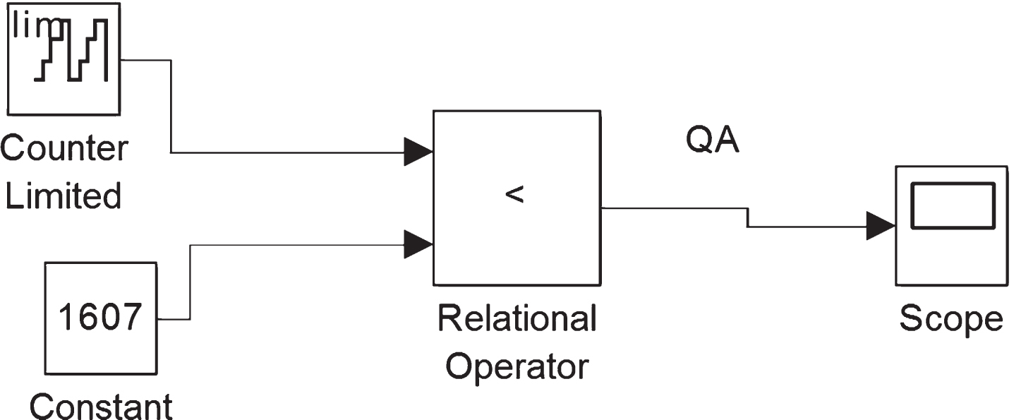
QA PWM program by Simulink.
The PWM structure formulated by the comparator and counter.
Simulation of Fig. 4a by Simulink tool.
Δt1 gap time shown in Fig. 2, assuming 60 step counts. QB square wave in Fig. 2 can be mathematically expressed as follows:
From (7) to (11), we can design a corresponding Simulink program shown in Fig. 5. The remaining QC and QD waves’ programs are designed in Fig. 6, where delt _ t3 ≜ Δt3 and delt _ t2 ≜ Δt2 are same of the one in Fig. 2.

QB PWM program by Simulink.
QC and QD of PWM program by Simulink.
Design four PWM square waves by Simulink software shown in Figs. 4–6 to meet the clock pattern of Fig. 2 where Δt3 is the simultaneously delay time of QC and QD PWMs. From Fig. 2, the range of Δt3 is
Controlling the delay time Δt3 is equivalent to control the overlap Δt4 of (QA, QD) and (QB, QC) two pairs of PWM waves, such that load output can approach to the reference input. Longer (Shorter) Δt3 is, shorter (longer) the overlap Δt4 is such that the DC load output V
o
becomes lower (larger). Therefore, the closed loop control circuit of Fig. 1 can be re-written as system block Fig. 7. We mathematically express hill-climbing control in Fig. 7 as below:
Constant voltage control.
where p of climbing step here is chosen as positive one, negative one or zero to guide the controlled output to reach the desired target, V o ≈ V r .
In Fig. 1, if the voltage V
o
is used as a feedback control signal, this control scheme is defined as a constant voltage control. On the other hand, since the voltage increasing or decreasing between the shunt resistance R
s
is proportional to the magnitude of the current flowing through the shunt R
s
according to Ohm’s Law. If using the terminal voltage V
s
as feedback signal, it can be regarded as constant current control shown in Fig. 8 whose mathematical expression are:

Constant current control.
Longer the climbing step p in (15) and (18), the shorter rising time to load output is. That is, from Figs. 7 and 8, we know that the DC output V
o
will quickly approach the desired one V
r
for a suitable magnitude step p. But the electroplating industry needs that the DC output should gradually and linearly reach the desired one at a preset rising time t
set
. In order to satisfy the electroplating factories’ demand of the slowly rising output of DC converter. This paper adds a linear saturation block behind the reference input signal whose schematic block is shown in Fig. 9. The linear saturation block is
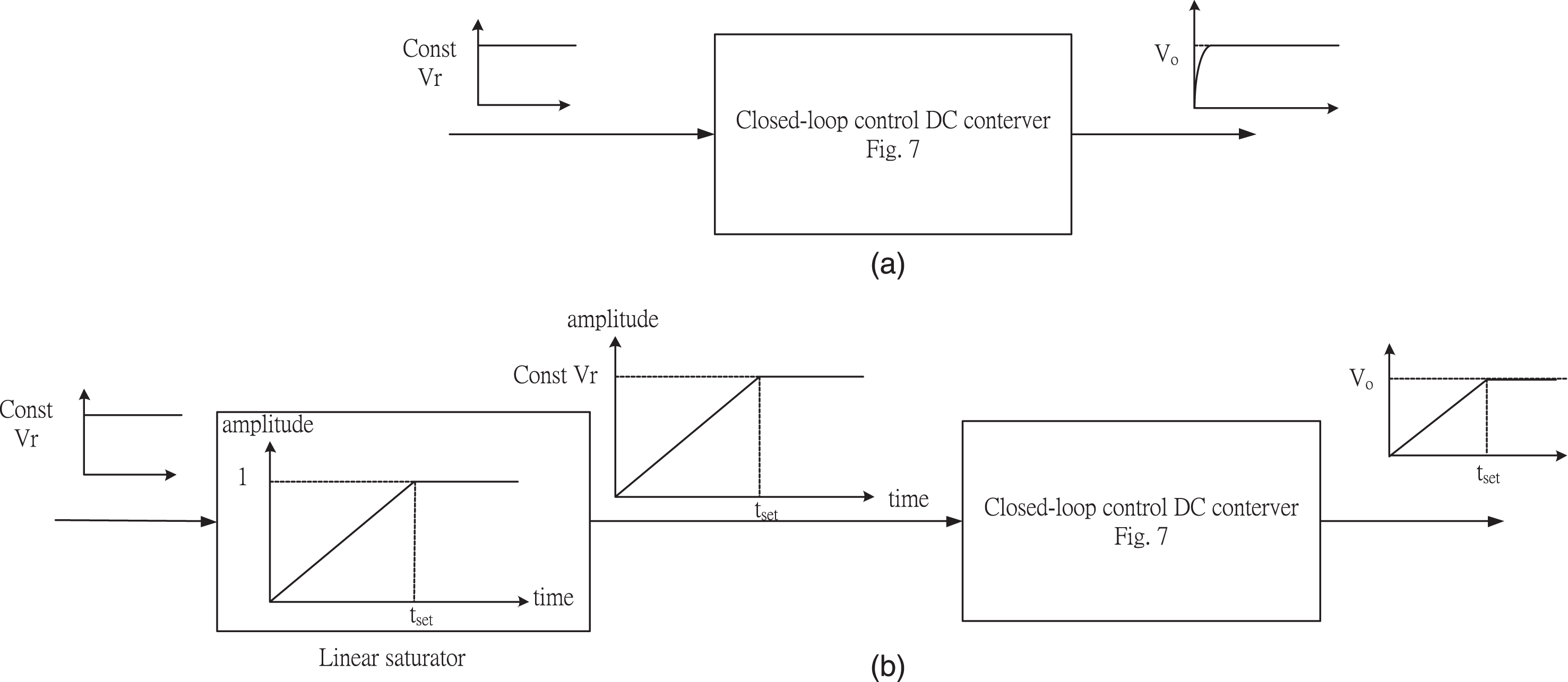
DC converter with slow rising control. (a) Original system output with fast response. (b) Gradually slow output response.
where t set is a preset rising time shown in Fig. 9(b). The output response of the original closed-loop system circuit Fig. 9(a) quickly reach the desired one. Take use of Fig. 9(a)’s function, add linear saturator behind the reference input to obtain the gradually slow output of the DC converter shown in Fig. 9(b).
In order to verify that the proposed control is feasible, the corresponding parameters of controlled full-bridge simplified circuit Fig. 1 are given below: input DC voltage V in = 220 Volts, inductance L o = 50uH, Capacitance C o = 82000uF, shunt resistance R s = 12/600 = 0.02 Ohm, turn ration of the center-tapped transformer is 26:1, all of the frequencies of QA ∼ QD PWM square periodic waves are 15KHz, A/D (Analog to Digital) sampling frequency is 2MHz, the maximum load current = 600A, maximum load voltage = 12 Volts, load resistance R o = 0.02 Ohm, the time interval Δt1 = Δt2 = 1.2 * 10-10 seconds of Fig. 2 are set.
The digital development board with Altera Cyclone IV FPGA chip is used in this paper. Experiment separately with the following items: Constant voltage control: The load output voltage V
o
can be controlled to follow a given reference voltage V
r
which is set 500 (indicates 5.00 Volts). Experimental results are shown in Fig. 10. Constant current control: The load current I
o
is controlled to approach the reference value which is set 100 (indicates 100 Amperes). The experimental situation and measurement data are shown in Fig. 11. Constant current control for slowly rising output: Reference input current 100 amps whose rising time are set at 7 seconds. That is, output current approaches 100 Amperes at 7 seconds. Its experimental measurement data are shown in Fig. 12. Zero voltage switching (soft switching): In the constant current 100 ampere control, we measure power switching element IGBT’s terminal voltage whose waveform shown in right of Fig. 13, no jitter voltage phenomenon. We also present a hard-switching plot with jitter in left of Fig. 13 as a contrast.
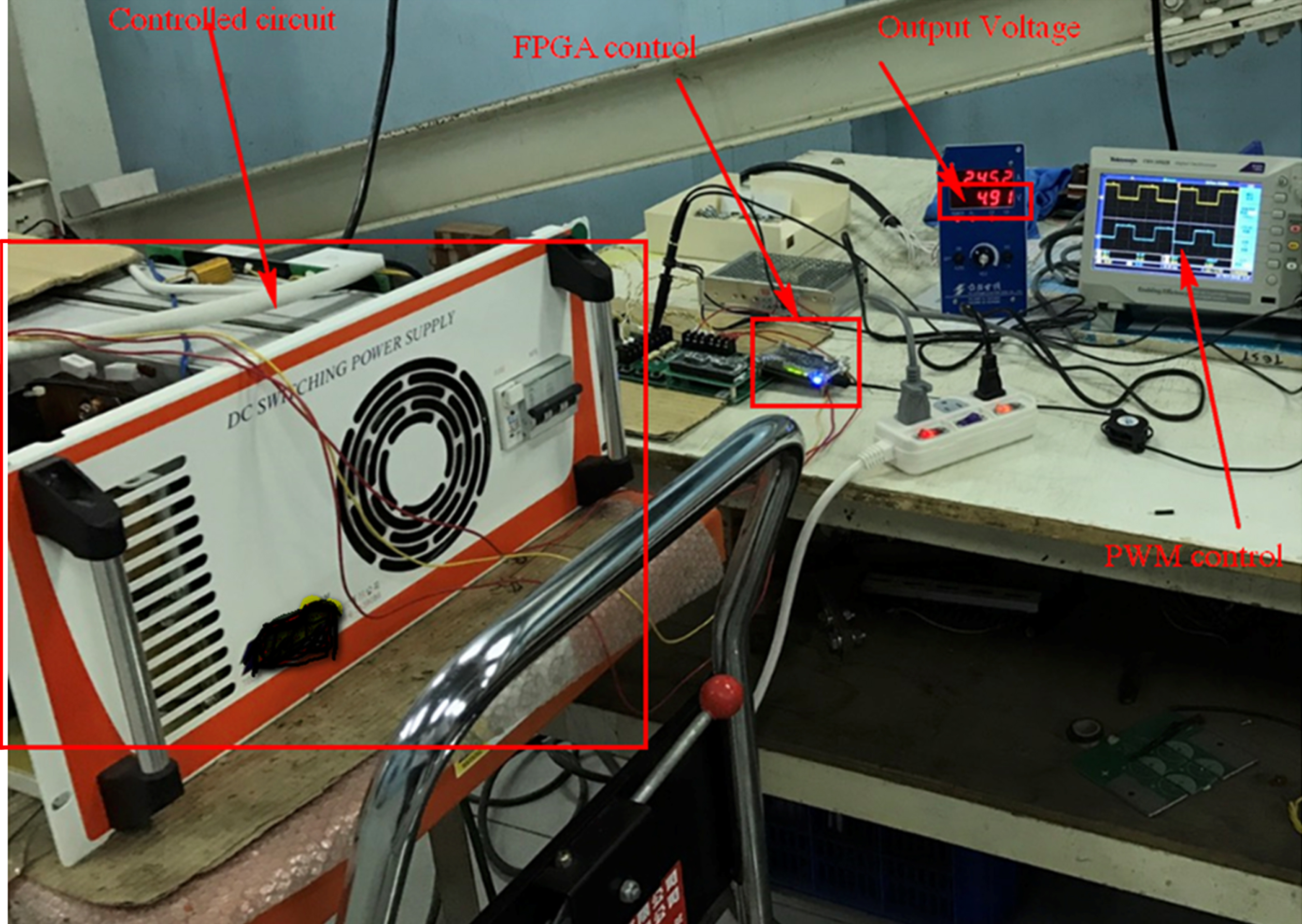
Constant voltage control for 5 volts reference input.
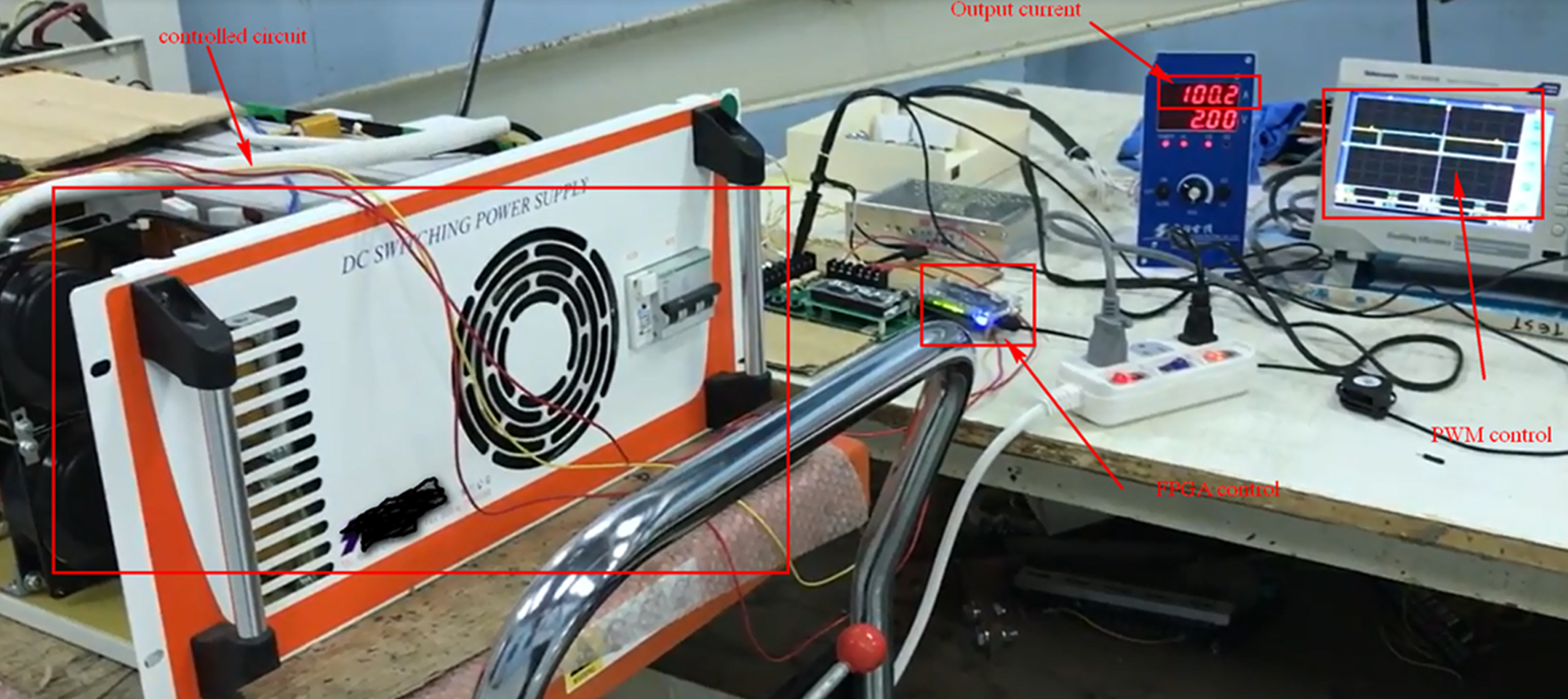
Constant current control for 100 Amperes reference input.
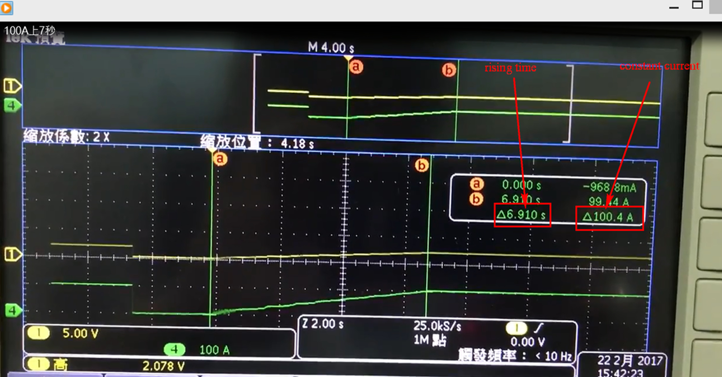
constant current control with slowly rising 7 seconds for 100 amps reference input.

Comparison between hard and soft switching under Constant current control of 100 Amperes.
From above experimental illustration, it is sufficient to demonstrate that the proposed digital controller based on the FPGA chip is feasible to constant voltage/current control of DC converter. It also can control the output to attain desired one at a preset rising time. Furthermore, there is soft switching function to achieve the benefit of energy conservation.
In this paper, we successfully implement a digital control based on the FPGA chip to accomplish constant voltage/current with slowly rising control for a 7.2 KW full-bridge DC converter circuit. The soft switching is also achieved to reduce energy consumption. The proposed HDL code is not directly written in Verilog language, but with Matlab/Simulink verification and then transform the Matlab/Simulink program into the corresponding HDL code. Its advantage is simultaneously to complete and verify the desired HDL code. Comparing digital programming and traditional IC design, we know the advantage of digital programming is: (1) it is flexible and can be updated at any time by language program; (2) saving hardware space; and (3) the development cost is reduced. This is why the digital program is the mainstream of modern industrial control.