
Abstract
Resistive random access memory (RRAM) has lots of advantages that make it a promising candidate for ultra-high-density memory applications and neuromorphic computing. However, challenges such as high forming voltage, low endurance, and poor uniformity have hampered the development and application of RRAM. To improve the uniformity of the resistive memory, this paper systematically investigates the HfOx-based RRAM by embedding nanoparticles. In this paper, the HfOx-Based RRAM with and without tungsten nanoparticles (W NPs) is fabricated by magnetron sputtering, UV lithography, and stripping. Comparing the various resistive switching behaviors of the two devices, it can be observed that the W NPs device exhibits lower switching voltage (including a 69.87% reduction in Vforming and a reduction in Vset/Vreset from 1.4 V/-1.36 to 0.7 V/-1.0 V), more stable cycling endurance (>105 cycles), and higher uniformity. A potential switching mechanism is considered based on the XPS analysis and the research on the fitting of HRS and LRS: Embedding W NPs can improve the device performance by inducing and controlling the conductive filaments (CFs) size and paths. This thesis has implications for the performance enhancement and development of resistive memory.
Keywords
Introduction
Nowadays, the Internet of Things, mobile devices, and machine learning are emerging trends that cannot be separated from memories, which offer new opportunities to memories, while conventional memories are facing the challenge of size scaling down [1], thus the emerging non-volatile memory (NVM), such as magnetic random access memory (MRAM), magnetic random access memory (FeRAM), phase-change random access memory (PRAM) and resistive random access memory (RRAM) appear at the right time [2]. And among those NVMs, RRAM exhibits significant potential for upcoming ultra-high density storage applications due to its advantages of high operation, low power consumption, stable endurance, and high integration, etc. [3–5] Additionally, it has been successfully demonstrated that RRAM-based neuromorphic computing accelerators can diminish the power consumption of heterogeneous computing systems and overcome the restrictions of the so-called “memory wall” [6]. The repeated formation and breakage of CFs is the most important conductive mechanism in the resistive switching phenomenon of RRAM. And many reports have researched the conductive mechanism of RRAM. Under the external electric field, the formation and rupture of CFs are similarly random, and the randomness of CFs results in the issue of poor uniformity restricting the mass manufacture of RRAM chips [7]. According to related literature, the forming process for RRAM also has some challenges: the high forming voltage not only affects the performance but also affects the integration of RRAM sub-20 nm. Meanwhile, a high forming voltage may make the design of peripheral circuits complicated [8–10].
To solve the problems of uniformity and high forming voltage, many methods including doping or embedding nanoparticles [11–15], multilayer structures [16], using 2D materials, etc. [17, 18] have been proposed. By S-doping HfOx to adding oxygen vacancies (Vo), Zhang et al. [19] increased the stability and uniformity of resistance changes. Zhao et al. [20] used graphene as RRAM switching layer to control switching at low power. Jeong et al. [21] improved the performance of Al2O3-based RRAM in resistance ratio, memory window, endurance and so on by inserting the Ni layer into the top electrode (TE) and switching layer. Among those methods for improving RRAM performance, embedding nanoparticles is considered an effective method to improve consistency, endurance, and other performances [22–24]. Chang et al. [25] improved the stability and retention characteristics by embedding Pt nanocrystals in TiO2 layer. Gao et al. [26] prepared alumina films embedded with silver nanoparticles to obtain hybrid CFs with good high-temperature stability. The local electric field was significantly improved and the switching voltage was effectively reduced. When embedding Ru NCs into AlOx dielectric layer, the RRAM performance of the on/off ratio and retention performance could be improved visibly [27]. Although embedding nanoparticles can improve RRAM characteristics, the uniformity still needs to enhance. While among these metallic nanocrystalline materials, tungsten is a promising material for W that can reduce the oxygen vacancy formation energy [28].
In this paper, HfOx-Based RRAM with and without tungsten nanoparticles (W NPs) fabricated by magnetron sputtering and UV lithography are investigated for nonvolatile-memory applications. The results show that NPs-RRAM exhibits lower operating voltage, more stable resistive switching behavior, and better endurance up to 105 cycles, and throughout the analysis, a potential switching mechanism is proposed. This subject adds depth to the research of metal oxide RRAM and has some bearing on raising RRAM performance.
Experimental
Figure 1(a) presents the structure of TiN/W: HfOx/ITO and the device is fabricated as follows: A SiO2 substrate is first ultrasonically cleaned with acetone, isopropyl alcohol, and alcohol to remove surface impurities. The bottom electrode (BE) TiN is deposited on the cleaned SiO2 substrate under an Ar/N2 atmosphere using Ti (99.99%) as the metal target. The BE pattern is realized by UV lithography and peeling. Two HfOx thin films are deposited on TiN with Ar/O2 atmosphere using HfO2 (99.99%) as the ceramic target. The W sub-layer (about 1-4 nm) is deposited between the two layers of HfOx under the Ar atmosphere using W (99.99%) as the metal target. To form the W NPs, a tube furnace is utilized to anneal for 40 minutes at 500°C, in the whole process of annealing, the N2 is maintained at 50sccm. The TE pattern is also achieved with UV lithography (Nanguang H94-30 double-sided UV lithography exposure system) and peeling, the optical micrograph of the structure is shown in Fig. 1(b). The cross structure is achieved by BE perpendicular to TE with UV alignment. Then, TE is sputtered by the indium tin oxide (ITO) ceramic target (99.99%). And BE TiN, dielectric layer W: HfOx, TE ITO is deposited by magnetron sputtering (Magnetron-ion beam combined physical deposition system radiation equipment, FGL560). And the thickness of TiN, W: HfOx and ITO layers is about 40 nm, 20 nm, and 150 nm, respectively. As a comparison, the HfOx device without W NPs is prepared with the same parameters. To test electrical characteristics a semiconductor parameter analyzer (Agilent B1500A, Santa Clara, CA, USA) is employed, during the test TE is applied a bias voltage, while BE is grounded, and the electrical tests were carried out in a closed chamber at normal temperature. Before testing electrical characteristics, the samples are baked at a low temperature (100°C) to remove the water vapor on the surface of the sample surface and reduce the impact on the electrical performance of the sample devices. Moreover, X-ray photoelectron spectroscopy (XPS, Scientific Escalab 250Xi, Waltham, MA, USA) is used to examine the composition of HfOx and W: HfOx thin films.
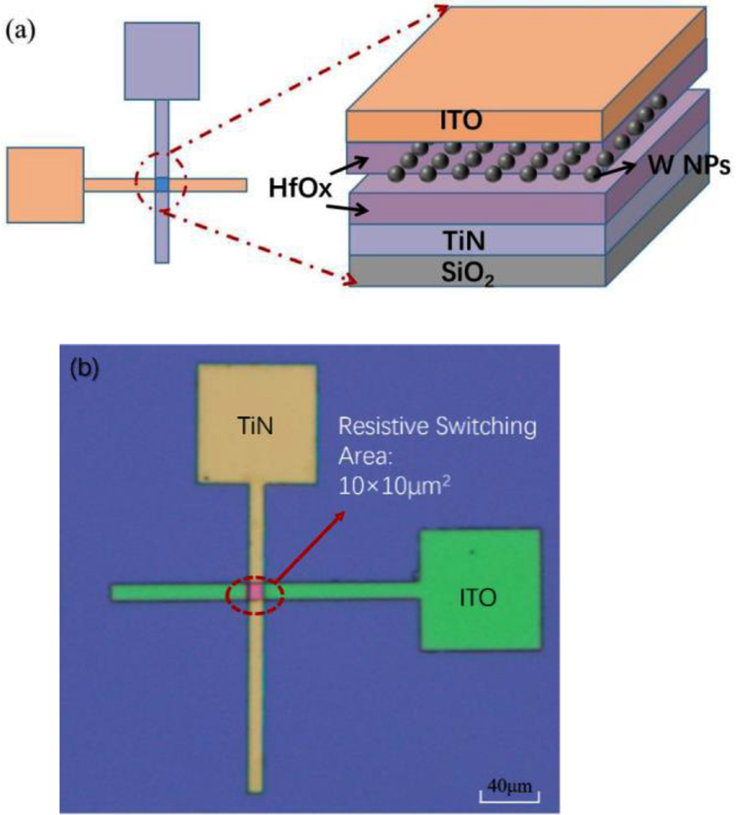
(a) The structure of the ITO/W: HfOx/TiN device. (b) The optical micrograph of ITO/W: HfOx/TiN device.
To verify the effect of the device performance embedding W NPs, two samples are prepared with the same conditions in this work, one with W NPs and the other without NPs, and the two samples are tested under the same conditions, the performance results of the two devices are compared, and the results are as follows:
Figure 2 shows the typical I-V switching characteristics of ITO/HfOx/TiN and ITO/W: HfOx/TiN devices. DC voltage scan is used during the forming process. Both ITO/HfOx/TiN and ITO/W: HfOx/TiN devices exhibit high resistance in initial states. Because a larger current can build strong CFs, here the compliance current (Icc) for forming is 100μA, too small Icc may result in unstable CFs [29]. It has been extensively reported in the literature that Icc can severely affect resistive switching behavior and due to thermally activated Vo external diffusion effects, too small Icc may lead to unstable CFs [30–34]. And the result shows that the W NPs device has a smaller forming voltage, and it suggests that embedding W NPs can reduce the forming voltage clearly. After the forming process, both devices exhibit bipolar resistive switching behavior, as shown in Fig. 2(b). It is noteworthy that the HfOx device exhibits poorer resistive switching characteristics during the DC voltage scan, including the set and reset voltages dropping from 1.44 V/-1.36 V to 0.7 V/-1.0 V. And the switching ratio is significantly larger than that of the HfOx device. Figure 2(c) displays the statistics of switching voltages. It can be observed that the W NPs device has lower switching voltages (Vforming falls from 5.31 V to 1.6 V, Vset drops from 1.44 V to 0.7 V, and Vreset from -1.36 V to -1.0 V). After forming process, both devices can reversibly achieve the set and reset process. The results suggest that W NPs are significant in reducing the device switching voltage. The reason is embedding W NPs can affect the energy of Vo formation and change the conductivity of CFs [35]. After calculating, embedding W NPs decrease the device’s forming voltage by 69.87%, which shows that embedding W NPs can thereby diminish the forming voltage and the energy required for Vo production [28].
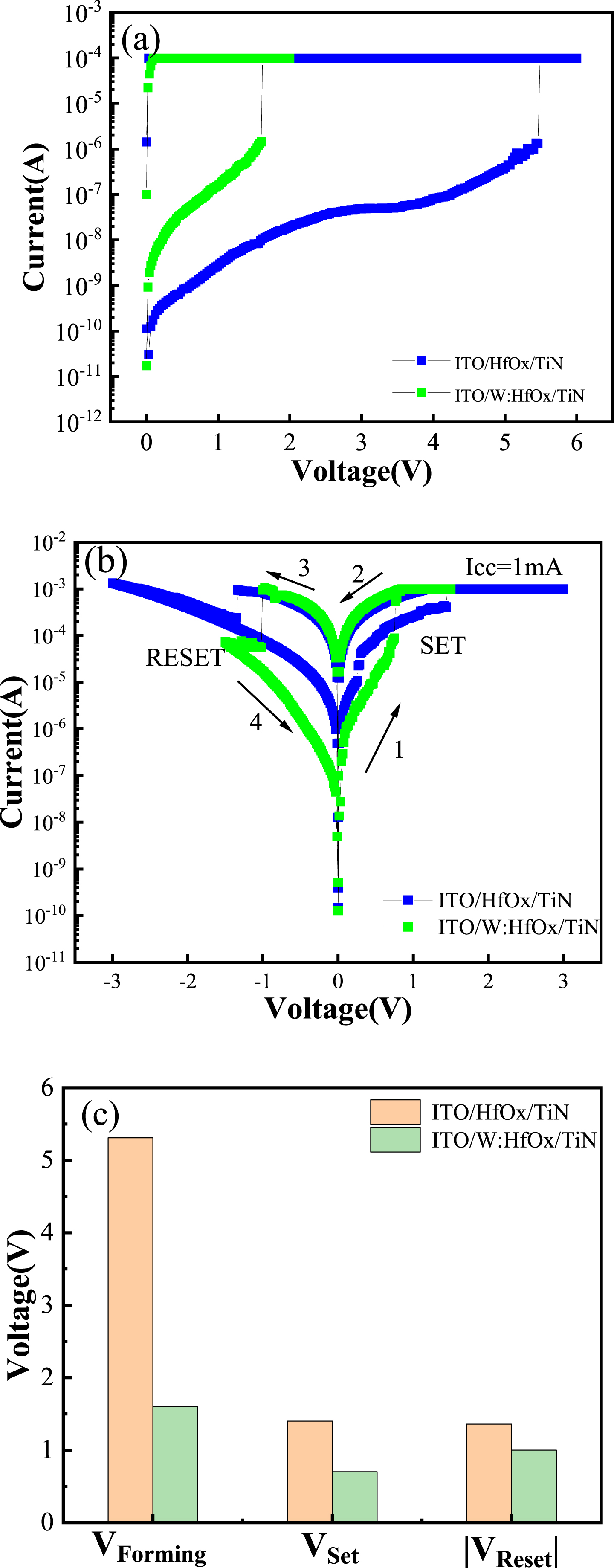
(a)The forming process current-voltage (I-V) curves of ITO/W: HfOx/TiN and ITO/HfOx/TiN devices (b) The I-V curves of ITO/W: HfOx/TiN and ITO/HfOx/TiN devices (c) The switching voltage of ITO/W: HfOx/TiN and ITO/HfOx/TiN devices.
The endurance is an important parameter to judge RRAM device performance, and the endurance of ITO/HfOx/TiN and ITO/W: HfOx/TiN devices are shown in Fig. 3. ITO/HfOx/TiN device has initial resistance values that are approximately 1200–1400 and 19k–31k, respectively. It can be seen that the endurance of the HfOx device fails at about 4×10⁴ cycles. While the initial resistance values of ITO/W: HfOx/TiN devices are about 1kΩ and 100kΩ respectively, and there is no noticeable change in LRS and HRS within 105 cycles. The endurance cycle characteristics of the two devices suggest that embedding W NPs can improve the number of repeated transitions between HRS and LRS of the device, the switching ratio of the W NPs device is increased by nearly 10 times, and the distribution of high and low resistance is more stable.

Endurance cycles (a) Endurance cycles of ITO/ HfOx/TiN device (b) Endurance cycles of ITO/W: HfOx/TiN device.
The cumulative distribution of set/reset voltages or HRS/LRS is one parameter to measure the uniformity of RRAM device. And Figure 4 displays the cumulative distribution of set/reset voltages and HRS/LRS. The W NPs device has a narrower Vset and Vreset range (Vset ranges from 0.68 V to 0.88 V, Vrest ranges from -1.0 V to -0.89 V) than the HfOx device (Vset range is 1.21 V to 1.74 V, Vrest range is -1.69 V to -1.27 V), indicating that the W NPs enhances the stability of the device’s set/reset process. What’s more, Fig. 4(b) shows that the W NPs device HRS/LRS has better resistance uniformity, and the switching ratio increases from about 14 to 100, the coefficient of variation (σ/μ, σ is standard deviation, and μ is mean value) of W NPs device exhibits narrower distribution than HfOx device as shown in Fig. 4(b) insert table, the results indicate that the W NPs improve the stability of the device [36].
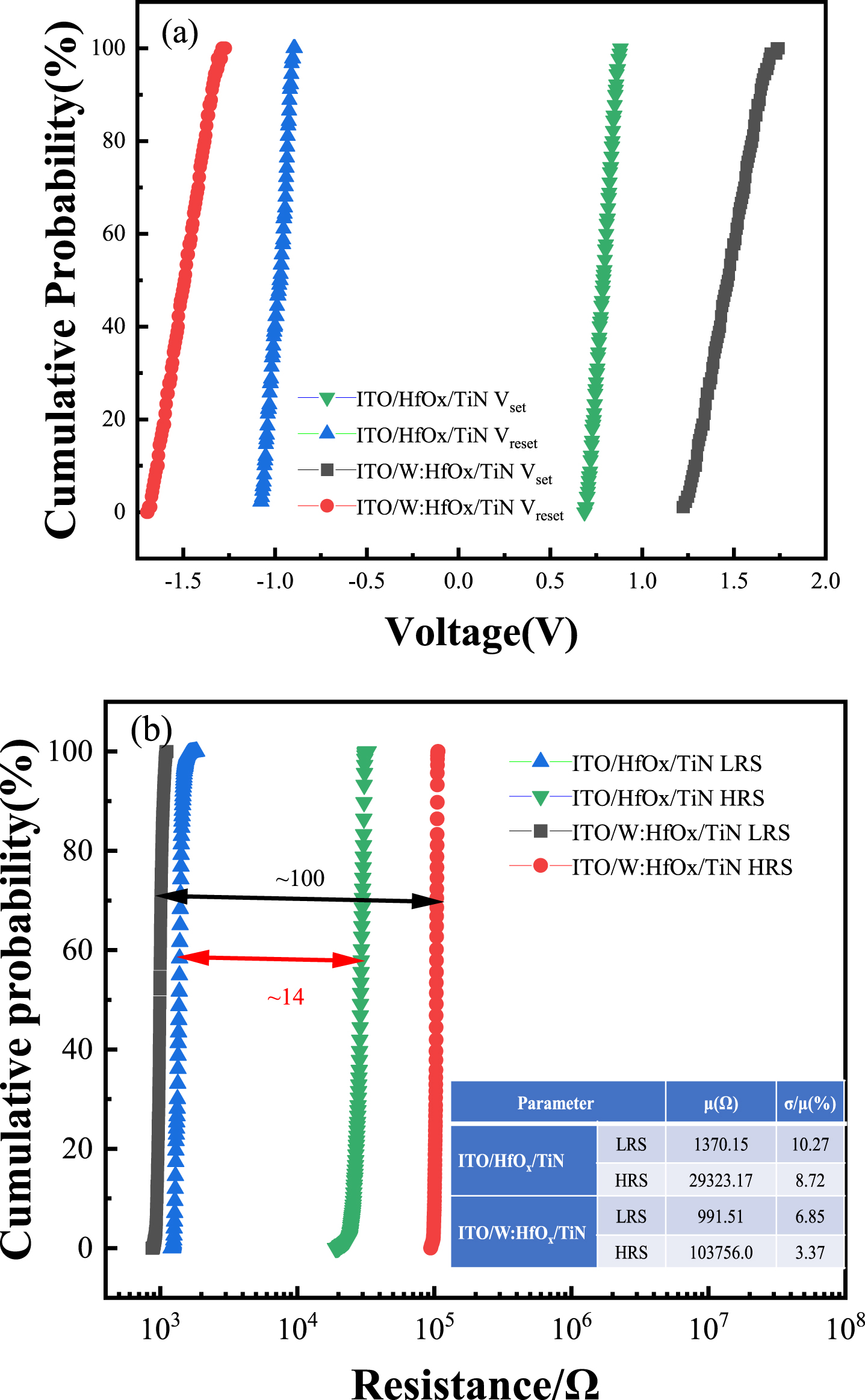
(a) Cumulative probability of set/reset voltage (b) Cumulative probability of HRS/LRS for ITO/ HfOx/TiN and ITO/W: HfOx/TiN devices.
Based on the analysis above, the W NPs device exhibits relatively better performance: lower switching voltages, higher switching ratio, more stable endurance, and uniformity. Table 1 lists the HfOx-based RRAM performance parameters in our work and compares them with previous reports.
Performance of HfOx-based memory RS devices, prepared in this paper and compared with previous reports
XPS is an effective way applied to study the compositions and chemical state. In order to investigate the intrinsic reasons for the improved performance of the ITO/W: HfOx/TiN device, the components of the devices were characterized by XPS. The bonding conditions of tungsten in W: HfOx films were investigated by XPS spectroscopy. The results are shown in Fig. 5. A standard calibration was performed during the XPS test using a C-C bond binding energy of 284.6 eV. Both devices Hf 4f can be well-fitted. Compared to HfOx films, the shift of the Hf peaks of the W: HfOx films toward higher binding energies is based on the NIST X-ray photoelectron spectroscopy database [43]. Since the CFs of the devices are formed by oxygen vacancies, the oxygen in the films is analyzed and Fig. 5(b)(d) shows the result. The peaks of O 1 s lattice oxygen in HfOx and W films are at 529.7 eV, and 530.2 eV, respectively. The percentage of area occupied is 62.25% and 56.16%. The non-lattice oxygen peaks are at 530.2 eV and 532.0 eV. The percentage of area occupied is 37.75%, and 43.84% respectively. The percentage of non-lattice oxygen is significantly increased. The results indicate that W NPs can increase the level of oxygen vacancies in the dielectric layer. And the increase in oxygen vacancies facilitates the formation and rupture of CFs during the resistance transition [44, 45]. Figure 5(e) shows the W 4f XPS spectrum in W: HfOx films with W 4f7/2 peaks corresponding to 30.5 eV, 32.6 eV, 35.7 eV, and W 4f5/2 peaks corresponding to 38.0 eV, 39.8 eV. Where the 32.6 eV, 35.7 eV, and 38.0 eV peak positions are consistent with W6 + and the peak at 39.8 eV corresponds to the W0 + state [46]. The W/O ratio was determined to be about 3.22 by integrating the W and O peak areas, and the results show that the contribution of the W oxidation state in W: HfOx films is due to the W6 +, and W0 +.

XPS spectra of HfOx films (a) Hf 4f; (b) O 1s; and W: HfOx films XPS spectra (c) Hf 4f; (d) O 1 s; (e) W 4f.
To further investigate the device switching behavior, a linear fit of the I-V curves for the high and low resistance states is performed using double logarithmic coordinates. The results are displayed in Fig. 6, it is evident that embedding W NPs does not alter the device’s mechanism. Figure 6(a)(c) shows the ln(I)-ln(V) linear fit of the LRS after the set, and the slope of the fit is approximately 1, indicating that the LRS follows an ohmic conducting mechanism, which suggests that the current of the storage cell in the low-resistance state is conducted through a CF [47]; Fig. 6(b)(d) shows the ln(I)-sqrt(V) linear fit of the HRS after reset, and the results are consistent with the Schottky emission mechanism, which results demonstrate that the HRS of the device exhibits a Schottky conducting mechanism.
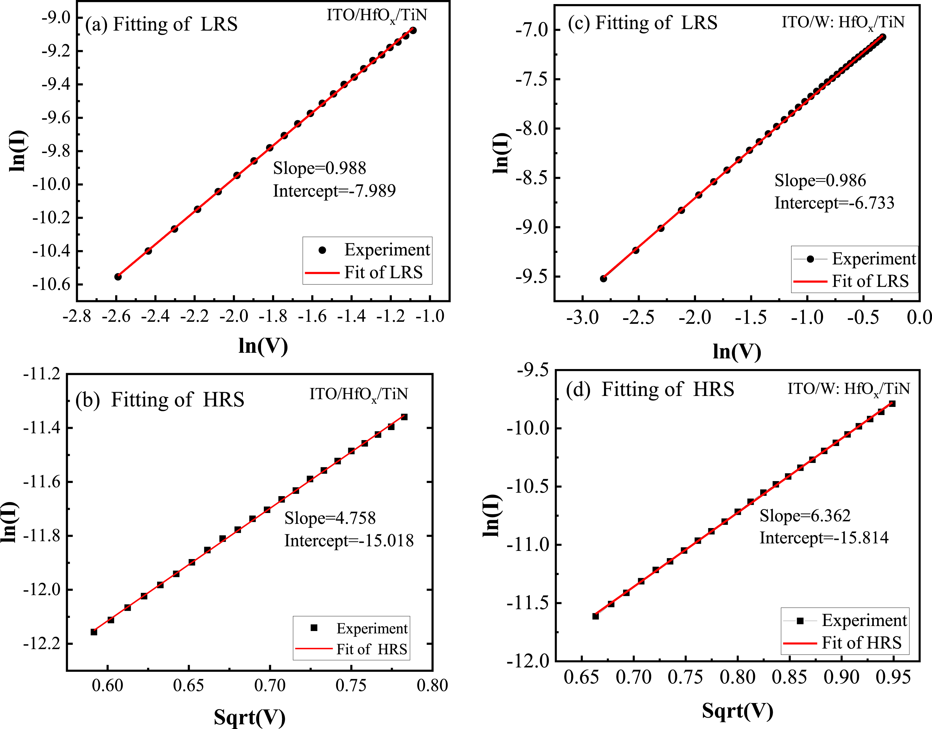
(a) LRS linear fit; (b) HRS linear fit and ITO/ W: HfOx/TiN device (c) LRS linear fit; (d) HRS linear fit for ITO/HfOx/TiN and ITO/W: HfOx/TiN devices.
Based on the mechanistic model, a possible resistive switching mechanism is proposed based on the XPS as well as the result of HRS and LRS linear fitting, as shown in Fig. 7. The formation and fracture of CFs are the main factors of resistive switching behavior. Regarding the HfOx device, as shown in Fig. 7(a)(b), the oxygen vacancies will move to the upper electrode ITO with a positive voltage, and a large number of oxygen vacancies form CFs in the dielectric layer. In this process, the movement of oxygen ions is affected by the Joule heat generated by the electric field, which creates a temperature gradient that causes the oxygen ions to diffuse randomly in all directions [48]. While a negative voltage will cause the oxygen vacancies to bind to the oxygen ions and the CF to break. After multiple resistance transitions in the device, some oxygen ions in the film become uncontrolled by the electric field and become unevenly distributed, resulting in unstable CFs, which deteriorates the device’s performance.

Schematic diagram of the switching mechanism of ITO/ HfOx/TiN device (a) set process; (b) reset process; and ITO/W: HfOx/TiN device (c) set process; (d) reset process.
And when embedding the W NPs into the HfOx dielectric layer, the tungsten divides the dielectric layer into two layers, as shown in Fig. 7(c)(d). Generally known, in the forming process of RRAM, the CFs will grow from random defects at the bottom electrode. In this work, embedding W NPs the CFs grow from TiN, while W NPs limit the path and size of the upper CF. The oxygen vacancy will move toward the negative electrode if applied a positive voltage to ITO/W: HfOx/TiN. The W interface has multiple stable oxide valences states attracting oxygen vacancy. Therefore, the upper electrode and lower W interface exist more oxygen vacancy. The tungsten atoms in the lower layer near W will take away the oxygen from the hafnium oxide and form more oxygen vacancies, which makes the CF formed in the lower dielectric layer wider and more stable, and the device will have a smaller resistance at low resistance. when the reverse voltage is applied, because TiN and ITO have the ability to store oxygen [49] and the top CF is thinner than the lower layer, the CF will begin to break preferentially in the upper layer around W, which explains why the device operates at a low voltage.
This paper examined the resistive switching behavior of embedding W NPs into hafnium oxide resistive devices that were manufactured using a magnetron sputtering process. W NPs device exhibits excellent electrical characteristics, including high uniformity, lower switching voltage, larger switching ratio (100), and stable endurance (>105). According to the experimental results, the improved device performance is attributed to the W NPs effect. Based on this, a possible conductive mechanism is proposed. Embedding W NPs can improve the device performance by inducing and controlling the size and paths of CFs. The findings show that other oxide-based RRAM may benefit from the use of embedding W NPs technology.