
Abstract
This paper present device model simulation describing the current-voltage characteristics of polymer/fullerene bulk heterojunction solar cell. In the research paper an organic photovoltaic device with PPV/PCBM [poly (2-methoxy-5-{3’,7’-dimethyloctyloxy}-p-phenylene vinylene) and {6,6}- phenyl C61-butyric acid methyl ester] was simulated via Silvaco TCAD 2-D simulation tool. PCBM acts as acceptor and PPV is donor. The models used to simulate the device were Langevin for recombination, s.binding and a.singlet. Simulation of these type of devices is an vital approach to project and predict the cell performance. Under the illumination of one sun (AM 1.5) the simulated organic cell showed a short circuit current density (J SC ) of 28 A/m2, open circuit voltage (V OC ) of 0.84 Volt and a fill factor (FF) of 52.51%, the resulting maximum efficiency of the PPV/PCBM organic solar cell is 1.22%.
Introduction
Solar cells based on semiconductors based are highly efficient devices for generating low cost eco-friendly, renewable form of energy. A solar cell converts sunlight energy into electrical power by producing photo-electrons in the solar cells active layer these photo-electrons give rise to the photo-electric current. The third generation of solar cells (Quantum dot and Organic solar cells) are the most encouraging field of photovoltaic cell research owing to their low fabrication cost and high flexibility. The photo-electrons are generated when a photon strikes the solar cell’s active layer or active area. If the energy of incident photon apt enough, then an electron by gaining energy from the photon moves to conduction band from valance band subsequently generating photo-current [1]. To propose a solar cell, numerical models are considered to be the tools of great convenance to comprehend the operation of solar cell and for its performance optimization for further applications [2, 3].
The organic solar cells based on the concept of BHJ (bulk heterojunction) are promising substitution for the traditional solar cells which are mostly based on silicon primarily due to their low cost and easy fabrication with great mechanical flexibility. In a BHJ based solar cell electron donating and an electron accepting material are intermixed and cast against a substrate, this creates a diffusing/penetrating web or mesh structure. The incoming solar light is absorbed by one material (electron donating material) which leads to the creation of an exciton. The dissociation of this exciton at acceptor-donor interface creating electron-hole pair which dispersed into two different media. The charge transport occurs via particular or individual material to respective electrodes [4, 5]. A bilayer solar cell has layered structure wherein electron donating layer is deposited on top of electron accepting layer. In bilayer solar cells maximum photocurrent is contributed by light absorbed near the junction only. This tricky problem does not exist in BHJ solar cells making them more promising concept than bilayer solar cells. In an article Mihailetchi et al. [6] established that parting of bounded electron/hole pair into free chare carriers is a significant procedure in solar cells. At very high reverse bias conditions photocurrent is saturated which demonstrations that all the electron/hole pairs are parted. The process of recombination can be omitted since at short circuit conditions the current is linearly dependent on the intensity of incident light [7, 8].
Goodman et al. [9] represented a model describing the abstraction of photogenerated charge carriers from a photoconductor. Barker et al. [10] represented a mathematical model describing the voltage-current characteristics of bilayer solar cell devices. The electronic structures of BHJ and bilayer solar cells are different thus their operational principles are essentially dissimilar. This article a device modelling is presented to characterizes the role of diffusion and drift of free charge carriers, contacts, junctions, carrier generation rate and recombination. In the present article, simulation, parameter extraction and internal analysis of PPV/PCBM based solar cell is carried out. The parameters obtained are utilized for the solar cell analysis using Silvaco-ATLAS numerical device simulator [11]. The fundamental performance parameters include open circuit voltage (V OC ), short circuit current density (J SC ), fill factor (FF) and power conversion efficiency (η). These parameters represent the quality of the solar cell designed and provide understanding of the solar cell’s operation. Further the solar cell is analysed in depth using vertical cut-line. Subsequently, potential distribution, electron-hole current density, recombination rate, carrier concentration is demonstrated. These cut-line based internal investigative studies are very crucial and helpful to understand the device behavior [12, 13].
This paper is divided into five sections including the introduction in first section wherein an explanation of device is carried out, which is followed by an analytical model representation with appropriate relevant equations in the second section. In third section the characteristic analysis of the BHJ solar cell is performed. In fourth section simulation results are presented showing the internal analysis of the device such as free charge carrier density and field distributions of the device. Finally, all the important results are summarized in the fifth section.
Device analysis & analytical model
An organic solar cell comprises of an active layer positioned among two electrodes with dissimilar work functions. This difference in work functions builds up an electric field (potential) in the active layer. The device is built up by a single semiconductor material with HOMO (highest occupied molecular orbital) of the donor and LUMO (lowest unoccupied molecular orbital) of the acceptor as conduction and valance band correspondingly. Figure 1 represents the structure of the BHJ solar cell and energy levels of the materials. In this article a BHJ solar cell was simulated with following materials layers ITO (Indium Tin Oxide), PEDOT: PSS, PPV/PCBM, LiF, Al respectively. The length of the device is taken to be 1μm. The structure is summarized in Table 1.
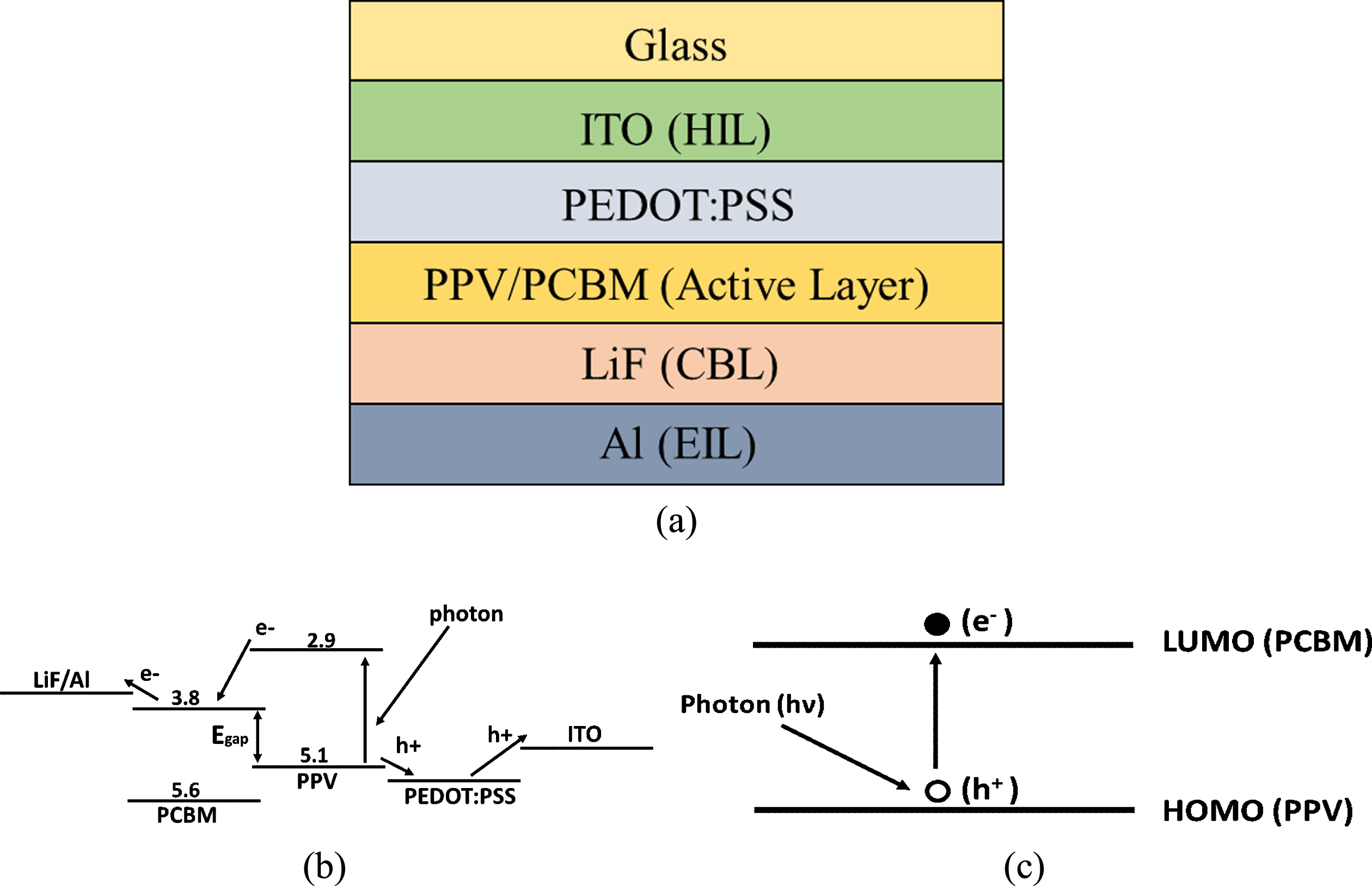
(a) Device structure of multilayered solar cell. (b) Illustration of energy levels of electron accepting and donating materials. (c) Representation of device under operating condition.
Thicknesses of the solar cell layers [14]
The ITO is anode for the solar cell also known as hole injection layer which is conductive and transparent in visible spectrum, the PEDOT: PSS is a flexible and conductive polymer for integration on an organic platform the material has high electrical conductivity, high transparency (88%), high elasticity and can be shaped into different geometries making it extremely suitable for microfabrication of organic platforms. The PPV/PCBM is the active layer in the BHJ solar cell. LiF (Lithium Fluoride) is an efficient cathode buffer layer (CBL) whose thickness is maintained below 1 nm and has insulating property. Aluminum (Al) is the cathode of the BHJ solar cell.
The difference of energy amid the donor material’s HOMO and the acceptor material’s LUMO denotes the band gap of semiconductor. The fact to be noted is that in an organic solar cell band gap isn’t a strictly defined quantity. The process of recombination is described by and its rate is specified by Langevin with the assumption that electron/hole pairs are generated at a homogenous rate throughout the device. The free charge carrier generation is a two-step procedure at first there is dissociation of exciton at the acceptor-donor interface yielding an electro/hole pair which is bounded, this bounded electron/hole pair is further separated into free electron and hole.
The device is defined by means of the metal-insulator-metal (MIM) picture. The basic equations describe the transport of charge carriers. Analytical model-based simulators are proven to predict and enhance the performance of the device before its actual realization. The simulation of the solar cell solves the basic mathematical equation with an objective to understand the solar cell’s performance. In the article the solar cell proposed is analyzed via benchmark industry standard Silvaco Atlas 2-D device simulator. The equations used in the article contains the drift and diffusion of charge carriers. The generation rate of electron-hole pair is presumed to be homogenous all over the device. To solve the basic equations the device simulator at first makes a presumption of potential and the density of the charge carriers, this is followed by a subsequent correction in value of potential calculated via Poisson equation. The corrected value of potential is added to the presumed value of potential and this process is a recurring process until a convergence point is reached. Further, in the next step carrier densities are calculated from the new value of the potential by solving continuity equation. This procedure is also of recurring character until convergence is reached.
The equations used in simulations are the Poisson equation [15, 16]
Where Φ (x) is the potential and p(x) is hole density and n(x) is the electron density, q is charge and ɛ is dielectric constant respectively.
The continuity equation is specified as
Where J e (x) is the electron current density and is the J h (x) hole current density. H(x) is net generation rate.
The net generation rate is the difference between generation of free charge carriers and their recombination.
The relation between the carrier densities to current densities (including both diffusion and drift) and the potential is given as
Where, D n and D p are the carrier diffusion coefficients.
At x = 0, device top contact exists, and at x = Z the bottom contacts exist. Z presents the device thickness and x presents position within the device. To obtain proper simulation solutions its essential to specify potential and free carrier densities at the contacts.
By using Boltzmann statistics,
Where, N c presents effective density of states for both valance and conduction band. As the precise values of effective densities of states of conduction and valance band are unknown, thus one value for both the bands is used.
Similarly,
The boundary conditions for potential are:
Where V s is applied voltage.
The generation and recombination theory explained by Onsager [17] and Braun [18] we can determine the net generation rate.
Onsager explained the generation on photocarriers, further enhancement to this theoretical model is made by Braun stating that bound electron/hole pair have a fixed determined lifetime.
The bounded electron/hole pair might degenerate to ground state through decay rate of K f or else dissociate into free charge carriers.
Probability of electron/hole pair dissociation according to Braun’s is given as
Where, K diss is dissociation rate constant, R’ is recombination rate constant, x is electron/hole pair distance, T is temperature and E is field strength.
Expression for K diss
EB is the electron/hole pair binding energy, J1 is Bessel function of order 1 and R’ is recombination rate defined as
Where, n int is intrinsic carrier density and ϒ is the recombination strength.
The equation used in Barker et al. [10] where X is number of bounded charge carrier pairs per unit volume changed in time is given by
In steady state
the above equation represents the total number density of free charge carriers generated, thus continuity equation becomes (for electron)
Using Equation (8), K diss =[P/(1-P)]K f , thus Equation (8) becomes
Further, continuity equation becomes
Finally, net generation rate is
Thus, after bimolecular recombination the charge carriers are not certainly lost, but form bounded electron-hole pair which either degenerate to ground state or dissociate into free charge carriers.
The simulators based on analytical models have demonstrated their vital and indispensable role to visualize and optimize performance of the device before their actual realization. In present section the BHJ solar cell is simulated and analyzed with an aim to extract the solar cell’s fundamental parameters so as to understand it’s performance and quality. Further, to comprehend the internal device physics and operation of the BHJ solar cell proposed benchmark industry standard Silvaco Atlas numerical device simulator [19, 20] is used. The simulator allows for materials and device structures to be user defined, offers various model parameters for accurate calculations and device behavior modelling meshing is incorporated [21–23]. All parameters that are used for the simulation of the device are itemized in Table 2.
The accuracy of the BHJ solar cell’s characteristics in the simulator (Silvaco-Atlas) originates from the amalgamation of diverse optical propagation models of robust nature. The simulator has built-in public domain AM1.5 & AM0 solar spectra which can be accessed by BEAM statement. Further, use of ray tracing model directly traces the accurate number of rays to determine any discontinuity at device surface or deep within the cell.
The Fig. 2 represents the experimental data attained from current-voltage measurement made on an OCC-PPV/PCBM bulk heterojunction solar cell [23]. In the graph the photocurrent density under illumination, is plotted as a function of the voltage (V), it must be noted that the experimentally gained value of open circuited voltage (VOC) is reported as 0.90 volts, this experimental value is very close to simulated value of 0.84 volts. Also, for comparison the experimental and simulated photocurrents are shown in linear plot which is focused on the fourth quadrant, it can be understood that the simulated photocurrent fits the experimental photocurrent data over the complete voltage range.
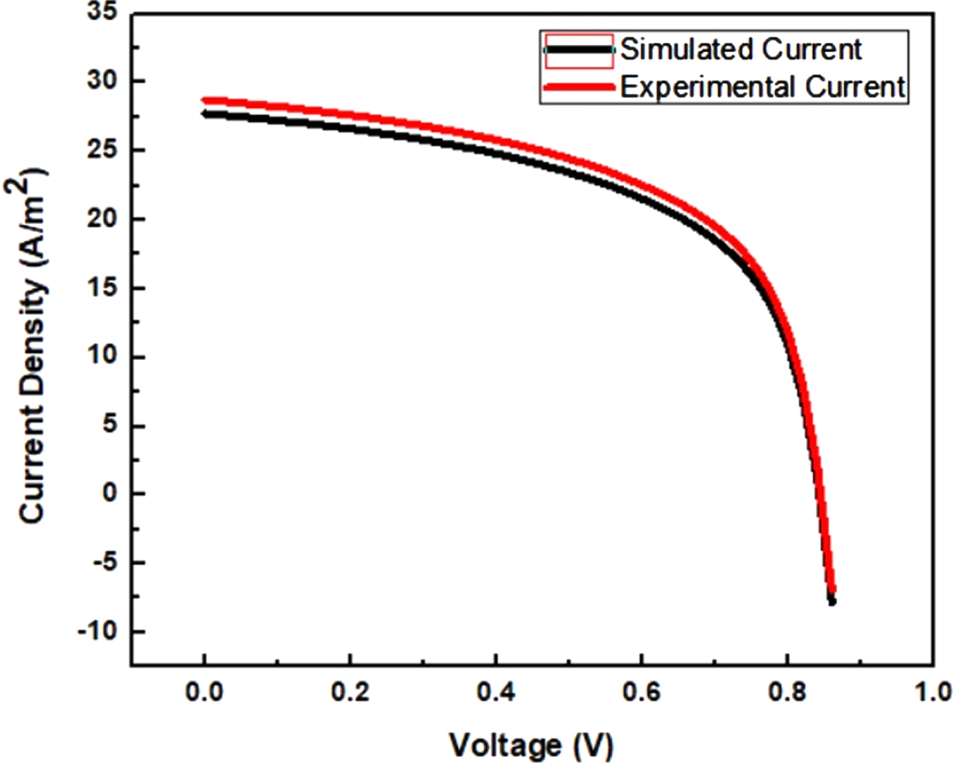
Current-voltage characteristics of photovoltaic device the red curve represents the experimental current and black curve represents simulated current.
The applied voltage reflects internal electric field of the device. The open circuit voltage can be stated as the maximum voltage generated by the solar cell when no connected to a load, at open circuit voltage the current density is observed to be negative as open circuit voltage is dependent on the lifetime of the minority chare carriers on both side of the junction, and the negative value presents the fact that the minority carriers flow is opposite to the flow of majority carriers. The maximum magnitude of photocurrent density is 28 A/m2 at zero voltage (short circuit current density). The short circuit current depends on multiple factors; such as, power of incident light, optical properties, Solar cell area and collection probability. From graph current density is constant till V(volt) and then it declines exponentially, thus the plot trails the universal I-V shape of a solar cell and is linear plot lying in the fourth quadrant. The Table 3 represents the all the extracted fundamental parameters of the BHJ solar cell.
Extracted performance parameters for the BHJ solar cell
This close agreement between the experimental and simulated data allows us to further analyse the behavior of the device in detail for understanding its device physics.
The solar cell is further analyzed internally via vertical cutline through the center of the device. This internal analysis authenticates the BHJ solar cell’s performance. The internal potential variation in the device is shown in Fig. 3(a) and it can be observed that potential is higher towards the anode remains almost constant throughout the device specially in the active layer and further decreases towards the cathode. The peak of potential is observed at device thickness = 0μm and has a value of 0.67 V. Also evident from Fig. 3(a) the electric field is constant throughout the device except at the contacts where it shoots up, as at the contacts carrier (electron and hole) densities high. At device thickness = 0μm and the field has a value of 4.1×10⁵ V/cm. Further, internal potential variation in each layer is shown in Fig. 3 via vertical cut-line analysis this exploration of each internal layer of the cell is beneficial to analyse the device physics in depth, this also validate the performance dependence of the cell on each layer. The Fig. 3(a) and 3 (b) the x-coordinate represents the device thickness in micrometers (μm) which extends from 0μm to 120μm. The y-coordinate in Fig. 3(a) presents the potential in volts and its corresponding variation in Fig. 3(b) is presented by the color variation wherein the top red color represents the x = 0μm with a value of 0.67 volt. Similarly, different colors represent the respective values of the voltage in the different layers of the device. The Fig. 3(c) represents the variation of electric field, the x-coordinate presents the device thickness, the field is maximum at the contacts and nearly constant in all the other layers as presented by different color variation in the Fig. 3(d) .

(a) Characteristic plot of potential vs device thickness (b) Device structure depicting variation of potential (c) Electric filed vs device thickness (d) Device structure depicting variation of electric field.
It can be observed from the internal analysis that the field in device is fairly high at short circuit conditions, this large field also explains the high extraction rate of the charge carriers. Additionally, because of insignificant space-charge effect the is electric field constant. Also, due to high electric field strength there is little loss of free charge carriers, which eventually leads to decent extraction of free charge carriers subsequently resulting in low carrier densities at short circuit. As, density of carrier is less, recombination becomes weak, thus recombination lifetime of carriers increases.
The Fig. 4(a) and (b) illustrate the variation of electron and hole current density and (c) and (d) show the variation of electron and hole concentration respectively. From above variation profiles it can be observed that electron concentration and current density is more towards the top (device thickness = 0μm) where anode is present. The peak value for electron current density and electron concentration is 8.8 × 10- 4 A/cm2 and 19.1 cm- 3 respectively. Similarly, it can also be observed that hole current density and concentration is more at the bottom of the device where cathode is present thus verifying the flow of the photocurrent in the device.
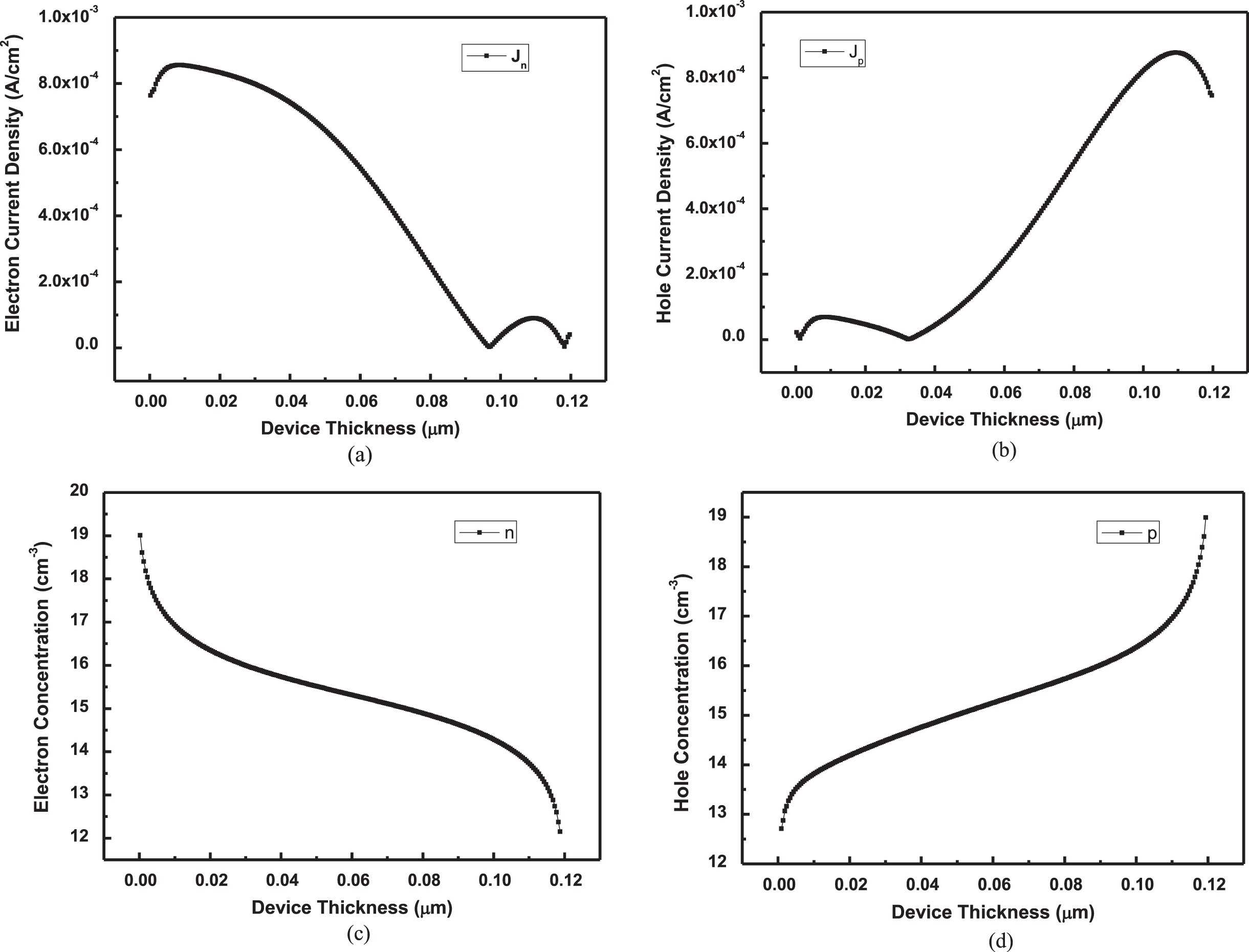
Characteristic plots of (a) electron current density (b) hole current density (c) electron concentration (d) hole concentration as a function of device thickness.
Further, from the variation profiles it can also be concluded that density of current displays linear dependency on the device position, though close to the device contacts both the charge densities are high and the process of recombination becomes extremely significant. In the bulk of the device hole density is larger than electron density due to difference in mobility amid holes and electrons. As holes are having low mobility than the electrons, they get concentrated inside the device. Also observed from Fig. 4(a) and 4 (b) that the current densities are nearly symmetrical this can be verified via Equation (3).
Rearranging the equation and using the Einstein relation,
Where, VT is the thermal voltage.
Then the Equation (3) becomes,
Integrating above yields
Now, using Equations (5.b), we get
Thus, verifying that the charge carrier densities are indeed symmetrical.
As per simulation result from Fig. 5(a) it can be observed that majority of all the free charge carriers recombine at the top layer near the anode and later decay. Rise in loss of free carrier is the consequence of lesser charge extraction, eventually leading to higher carrier densities and increase in recombination probability. Further deep inside the device and in active layer the recombination rate is almost constant. The Fig. 5(b) depict the recombination rate which attains maximum value of 3 × 1022 cm- 3s- 1. The maximum recombination’s takes place in the active layer. Further, a decline in recombination rate confirms that holes and electrons are confined in active layer. Additionally, a decline in the recombination rate validates presence of maximum number of charge carriers at the active layer.
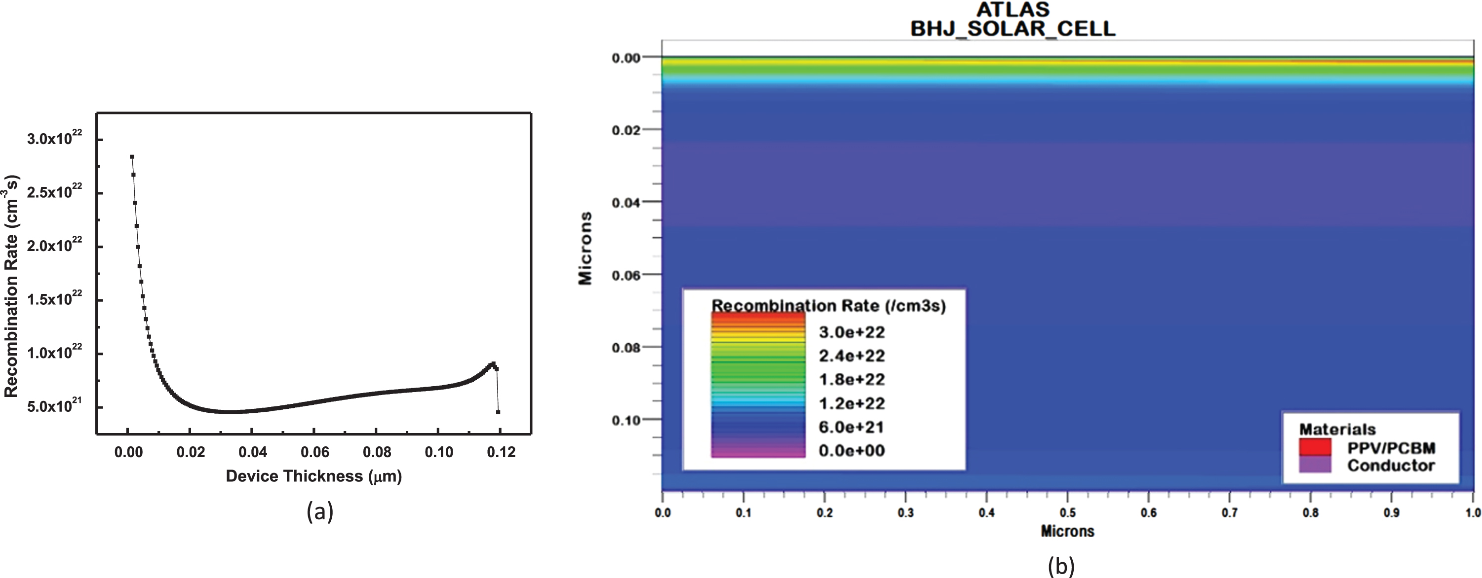
(a) Characteristic plot of recombination rate vs device thickness (b) Device structure depicting variation of recombination rate.
Further, the number of carriers lost via recombination can be calculated by calculating the net generation rate (H) which is obtained by integrating the Equation (2.a),
which gives
From Fig. 2. (a) we can determine J n (Z) to be equal to 0.4 A/m2 and J n (0) to be equal to 7.6 A/m2. The q is the charge and Z (device thickness) is equal to 120nm. This gives the net generation rate (H) to be equal to 3.75 × 1027 m- 3 s- 1 which is very close to the experimental value of 1.56 × 1027 m- 3 s- 1 [14]. Thus, presenting a agreement between the simulated and experimental data and verifying the behavior and internal device physics of the solar cell.
In this work, successful design and numerical simulation for ITO/PEDOT: PSS/PPV-PCBM/LiF/Al bulk heterojunction solar cell was performed using Silvaco Atlas numerical software and fundamental parameters such as short circuit current, open circuit voltage etc. were extracted. Further, a vertical cut-line analysis is performed to examine the internal device physics of the BHJ solar cell. The simulation results included the profile plots of charge carrier, the potential variation plot through the device, recombination profile. In the simulation JSC of 28 A/cm2, VOC of 0.84 volt and FF of 52.51%was obtained and these simulation results are in complete coincidence with the experimentally reported results and hence give an inside and in-depth view of the BHJ solar cells device physics.