
Abstract
OBJECTIVE:
At present, Internet of things (IoT) technologies such as radio frequency identification devices (RFID) have been widely used. In such context, manufacturing industries of semiconductor integrated circuits have gradually realised that it is necessary to integrate IoT technologies such as RFID with other systems of technologies. The research provides a new idea for the deep integration of IoT technologies including RFID with new-generation information technologies (IT) such as big data and deep learning and drives IoT technologies to develop with multiple functions and diverse types.
DESIGN, METHODOLOGY, and APPROACH:
The research takes the manufacturing enterprises of semiconductor integrated circuits as the objects and integrates IoT technologies involving RFID and intelligent sensors with new-generation IT technologies such as big data, sensing database, deep learning, knowledge discovery, etc. On this basis, a process innovation mode based on the integration of IoT and sensing big data is established. Based on the characteristics of sensing big data of enterprises manufacturing semiconductor integrated circuits, the innovation mode is designed in three stages including: data integration and fusion, data optimisation and modelling, and data application. Moreover, the system architecture, key technologies, modelling process, and algorithm design are also analysed.
FINDINGS:
A process innovation mode of semiconductor integrated circuit products based on the integration of IoT and sensing big data is provided.
Keywords
Introduction
Data volume and the multitude of sources have experienced exponential growth, creating new technical and application challenges in the manufacturing sector (Bello-Orgaz et al., 2016). These data come from everywhere in the manufacturing supply chain: product design, manufacturing, product operation, marketing and sales, and quality control processes. Meanwhile, the application of technologies such as internet of things (IoT), enterprise resource planning (ERP), manufacturing execution system (MES), product data management (PDM), etc. in manufacturing enterprises further increases the volume of data to be managed by these manufacturing enterprises. There has been a compelling need to adopt data management systems in industrial operational processes and product development principles to enhance IoT applications (Bevilacqua et al., 2017). It has been widely recognised that these technologies are interdependent and should be jointly developed (Chen et al., 2014). Therefore, data collected using IoT technologies such as RFID and intelligent sensors can be used for supply chain whole-process tracing and warning (Scalia et al., 2016; Liu et al., 2012) and improving the sales volume (Rizzi et al., 2016; Bottani et al., 2016). In addition to this, they can also be fused with new-generation information technologies (IT) such as big data and be integrated with systems including ERP, MES, and PDM to improve and innovate the processes used in manufacturing.
A series of new process technologies and modes have appeared with the advent of the age of big data, the maturity of the basic architecture of the Internet, and the promotion of the IoT and cloud computing technologies (Zhang et al., 2016). In that context, how to find innovative modes of processing for products using the Internet, IoT, and big data technologies has become an important approach for manufacturing enterprises as they develop and innovate, search for a rational the basis for their decision-making, and improve their competitiveness (Gao et al., 2011). Process innovation modes refer to how a new or modified production process is used in commercial production, and it is actually the application of new or significantly modified production modes (Wang et al., 2017). As a critical component of technological innovation, process innovation pays more attention to the process of the innovation compared with the product innovation. The maximum value of the application of technologies including IoT and big data, from the point of view, lies in that it provides more innovative possibilities for process technologies and production methods in practice.
The semiconductor industry, as the core of the IT industry, is a mainstay industry for promoting the transformation and upgrade of traditional manufacturing industries and for lifting the level of intelligent manufacturing. For this reason, the technological level and degree of innovation of this industry have become a standard for measuring the industrial competitiveness and the comprehensive power of a nation (Wang et al., 2017). The manufacturing of semiconductor integrated circuits involves extremely complex processes. Semiconductor integrated circuit products have exacting requirements imposed on the allied process technologies and modes, especially with regards quality and reliability, therefore, the application of the technologies, knowledge, and methods of IT including big data of the products can also meet the requirements of manufacturing industries of most of other high-tech products (Jian et al., 2016). So, the enterprises manufacturing semiconductor integrated circuits are typical and representative in their process innovation modes. Among them, integrated circuits are the most complex and representative of this type of device. Semiconductor integrated circuits are integrated circuits designed according to certain functions and are laid out by forming semiconductors with silicon or germanium substrates via doping with boron, phosphorus, etc. These semiconductors are produced as the base material taken from components such as resistors and capacitors and other connecting components. The whole process, including design, development, and production, of semiconductor chips is complex and dozens and even hundreds of specific integrated circuit chips are manufactured and mounted on a wafer with semiconducting silicon as the substrate. Semiconductor integrated circuits are typical knowledge-intensive and technology-complex products. Semiconductor integrated circuits, as the basis for the entire IT industry, are such that process innovation is critical to global socio-economic development (Wang et al., 2017; Jian et al., 2016). Taking the manufacturing enterprises of semiconductor integrated circuits as the objects of this research, we explored a process innovation mode based on the integration of IoT and sensing big data. We focus on the application process of IT technologies such as IoT and big data in manufacturing enterprises of semiconductor integrated circuits and the course of the process of innovation therein. The objective of the research is to provides a framework for the deep integration of RFID technology with big data and deep learning in the manufactures supply chain following three innovation process stages: data integration and fusion, data optimisation and modelling, and data application. The following two issues are mainly discussed: 1) the main characteristics of process big data of manufacturing enterprises of semiconductor integrated circuits compared with other manufacturing industries; 2) the detailed workflows including system architecture, key technologies, modelling process, and algorithm design of the process innovation of those making semiconductor integrated circuits.
Literature review
Big data integration with the Internet of things
The IoT is the network of physical devices, vehicles, home appliances, and other items embedded with electronics, software, sensors, actuators, and network connectivity which enable these objects to connect and exchange data. It includes information and sensing equipment such as RFID + Internet, GPS, laser scanners, and intelligent sensors. It is designed to connect network terminals with objects in their surroundings (involving information collection, co-processing, intelligent network, and even information servicing of sensing equipment), so as to identify, trace, and control the objects and form an intelligent system. Recently, some have tried to integrate big data with IoT technology to manage equipment manufacturing data and improve processing systems. Huang et al. (2016) analysed six aspects in manufacturing process control system–predicting, resource management, load balance, risk assessment, operations planning and process optimizing by the combination of big data technology and IoT technology. Wang et al. (2016) proposed a weighted network which regards the potential quality failure factor as a node and the relationships between the potential quality failure factors and complex network theory. Bevilacqua et al. (2017) proposed a framework to integrate IoT-based energy management and existing corporate information systems by big data analytic methodologies. Li et al. (2017) pointed out that the bottlenecks faced by enterprises in manufacturing IoT and big data analytics require a scientific workflow management system based on cloud manufacturing service platform.
Informatisation and process innovation of manufacturing enterprises
Research into modes of innovation remains in its preliminary stages: previous studies in recent years reveal that the extension of informatisation enriches the resources of manufacturing enterprises and gradually becomes a strategic core resource for the process innovation, so it is of great significance for increasing process innovation capacity (Gao et al., 2011). The Industry 4.0 paradigm takes, informatisation as providing infrastructures such as networks, computers, and automatic production equipment for organisations carrying out process innovation and becomes a powerful means for the process innovation among manufacturing enterprises. At the same time, it changes the mode of process innovation and reconstructs the procedure of process innovation (Gao et al., 2011; Tao et al., 2014). Adrien et al. (2000) believed that the integration of micro-electronics, computers, and automatic technologies with process equipment forms informatised process technologies at different levels changing from rigidity to flexibility and from simplicity to complexity. The integration also impels enterprises to introduce these informatised technologies to realise process innovation (Li et al., 2016). At present, how to construct a process innovation architecture to adapt to new changes in process innovation for manufacturing enterprises under an informatisation background has become a key problem to be solved (Adrien Presley et al., 2000). In the age of big data, integrating advanced IT technologies including the Internet, IoT, cloud computing, and big data and applying them in the process innovation during the production of manufacturing enterprises has produced many benefits. It is not only conducive to improving process innovation capacity and building intelligent production lines, but also to promoting informatisation and constructing an architecture for process innovation among manufacturing enterprises (Gao et al., 2011; Tao et al., 2014).
Existing research mainly focuses on the application of IT technologies such as IoT, big data, and cloud computing in quality control and enterprises’ decision making (Bevilacqua et al., 2017; Tao et al., 2014). Studies on the informatisation and process innovation of manufacturing enterprises also involve clarification of relationships between informatisation and process innovation on one side and an analysis of the influence of informatisation on the architecture of process innovation of manufacturing enterprises on the other: however, the comprehensive application of IoT technologies such as RFID and new-generation IT technologies such as big data in process innovation has seldom been studied. Currently, IoT technologies including RFID are becoming more widely used. Many enterprises, especially those manufacturing high-tech products (typically, semiconductor integrated circuits) have realised that integrating IoT technologies such as RFID with other systems and technologies is a key to achieving the development of IoT technologies with multiple functions and diverse types. Taking manufacturing enterprises of semiconductor integrated circuits as our object of interest, we aimed to integrate IoT technologies such as RFID and intelligent sensors with big data, sensing databases, deep learning, and knowledge discovery to explore a new process innovation mode.
Analytical framework
Semiconductor integrated circuits are technology-complex and knowledge-intensive, characterised by long production cycle, high value, and high risk. The whole production process of a semiconductor involves a complex process to fabricate dozens and even hundreds of specific integrated circuit chips on the wafer made of semiconducting silicon. The whole process consists of nine procedures (Fig. 1). Among them, wafer fabrication comprising thin-film technology, a rounding process, doping, and heat-treatment, is key to manufacturing of semiconductor integrated circuit products. The process of wafer fabrication is just like building a house layer-by-layer, and the layers are portioned by lithography. Each layer includes the combination of various processes such as deposition, lithography, etching, ion implantation, and metallisation, so each product is fabricated through at least hundreds of processes. In the operation, each process generates much complex, multi-source data (Zhang et al., 2016; Wang et al., 2017; Jian et al., 2016).
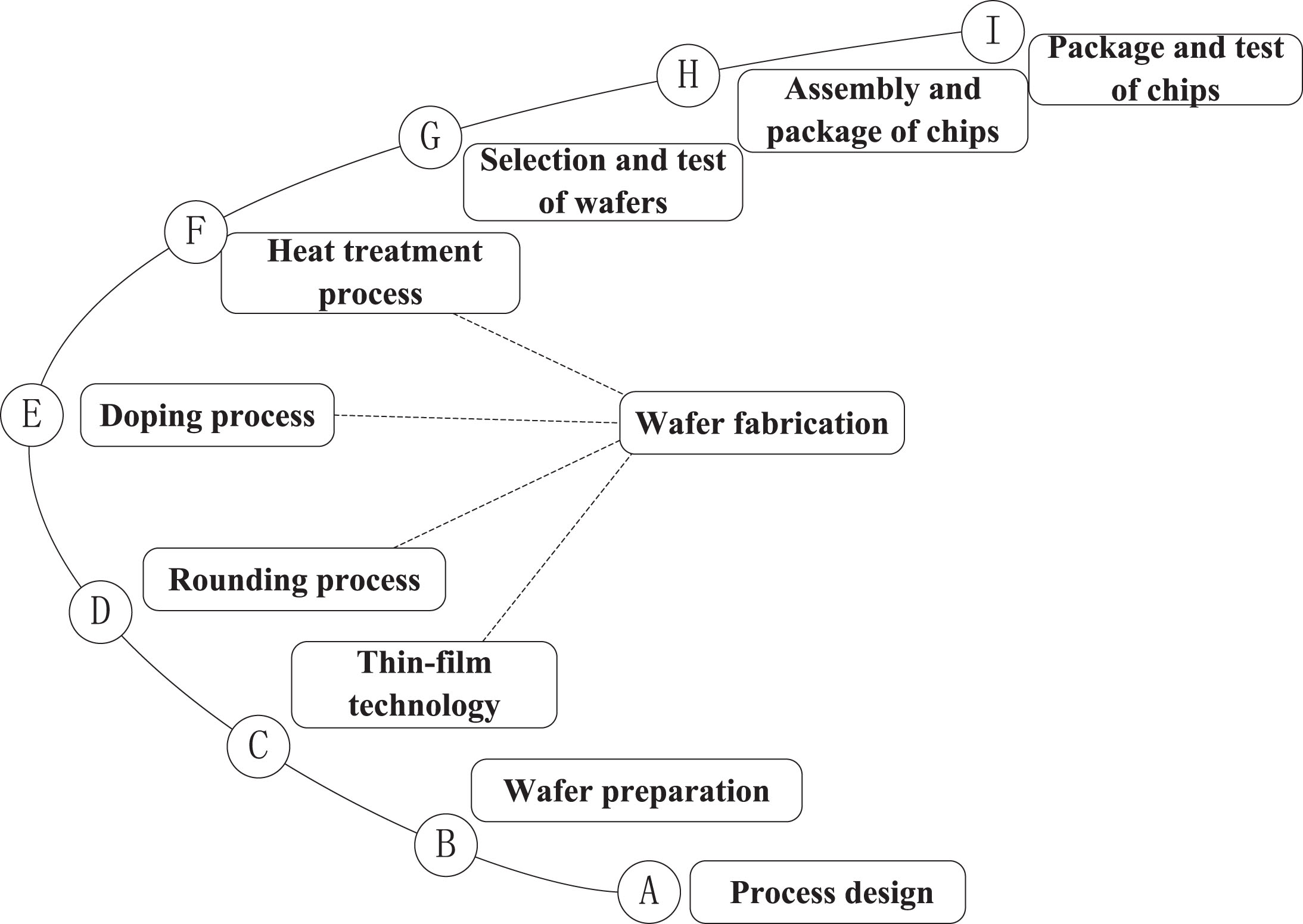
Technological processes in semiconductor integrated circuit manufacture.
The core competitiveness of semiconductor integrated circuits products lies in their technologies while technological development depends on the process innovation mode and development level. The complex and precise characteristics in the manufacturing process of semiconductor integrated circuit products can determine that the manufacturing processes have complex cyber-physical properties and operating characteristics of high value-density. At present, almost all enterprises of semiconductor integrated circuits in the world have used information systems such as ERP, MES, PDM, and APC, and their networking and informatisation have been realised in the manufacturing workshops. Data about manufacturing process, technology, quality, and logistics information are transmitted over the industrial Internet. The manufacturing technology of semiconductor integrated circuits is largely computer-controlled and such processing technologies have become highly automated. Based on the highly automated machines for producing semiconductors, various sensors are installed on the production lines to collect all kinds of data resources which are then transmitted through the Internet and the IoT, providing support for the operation of manufacturing information systems; however, the production of semiconductor integrated circuits is both precise and complex, especially during wafer fabrication, which involves various diverse processes. It is difficult to control the production line and guarantee the orderly running of the technological process: the process demands the further optimisation of the technological process and further technological improvement. We analyse and design a process innovation mode based on the integration of IoT and sensing big data and its key technologies, modelling, algorithm, and knowledge discovery in three stages (data integration and fusion, data optimisation and modelling, and data application). A process innovation mode of semiconductor integrated circuit products based on the integration of IoT and sensing big data is provided.
Characteristics of process big data
As the level of automation of machines in enterprises manufacturing semiconductor integrated circuits increases, and the collection of production process and technological parameters of wafers and chips become more automated, the volume of data increases. Owing to traditional PDM and ERP systems having limited optimisation scope for resources, they cannot timeously, and perfectly, deal with the huge volumes of process parameters generated in the production of semiconductor integrated circuits. So, it is necessary to use corresponding big data technology to analyse process data. Semiconductor integrated circuits involve a great variety of process parameters and up to 70 parameters are collected using single RFID and intelligent sensor for one item of equipment in a production line for wafer fabrication, and more than 400,000 pieces of data are collected every day. In general, there are about 500 items of equipment in a production line for wafer fabrication, so the data volume acquired in the production line of wafer fabrication is already large (Zhang et al., 2016). Moreover, as the production of semiconductor integrated circuits requires a long cycle and uses complex technologies, the data volume formed in the production process also increases. All these require all kinds of sensors to collect continuously and accurately huge amounts of data, so as to monitor the whole manufacturing process flow of semiconductor integrated circuits.
Classification of IoT-based sensing big data
Various RFID and intelligent sensors are employed to acquire data from the manufacturing systems and productions. These automated data from the sensors and industrial IoT are called IoT-based sensing data. The data can be acquired through manual typing, file import, direct data upload through equipment in various production links, typing using scan guns, RFID scanning data, and data integrated using other systems such as MES and ERP. IoT-based sensing big data can be classified into three types: identification data, that is, the data collected using RFID. The radio frequency tags of RFID are embedded in materials to traverse the whole production process. Within the sensing scope of the RFID antenna signals, the RFID sensors installed in production equipment can obtain each material tag and therefore fulfil the whole-process tracking of the materials. The tracking system based on RFID needs to acquire and process the tag data and correlate the tag data with equipment data. The system acquires and publishes tag data using the middleware layer, and correlates and processes the material and equipment information using the tracking layer for the production process. The second is status data, that is, data collected using intelligent sensors. These sensors are mainly used to collect all kinds of sensing information in the production process. By using these sensors, the production states of equipment and machines for semiconductor integrated circuits are remotely monitored. These two types of data are the most common, basic, and important data of IoT-based sensing big data. The third type is instruction data: commands can be given by human beings or automatically by systems (Wang et al., 2017). These data are generally used to represent a series of changes in system states.
Characteristics of IoT-based sensing big data
These IoT-based sensing data have inherent characteristics and processing requirements (Table 1).
Characteristics of quality control data in the wafer fabrication of semiconductor integrated circuits (Zhang et al., 2016)
Characteristics of quality control data in the wafer fabrication of semiconductor integrated circuits (Zhang et al., 2016)
1The data reflect whether the grains meet the functional requirements or not, so the data need to meet the functional requirements in the processing.
Big data exhibit typical 4 V characteristics, that is, variety, volume, velocity and value. As displayed in Table 1, the variety of big data sensed by manufacturing enterprises of semiconductor integrated circuits is mainly shown as the variety of data sources, types, forms, dimensions, and scales. The volume is generally reflected by the large scale of parameters, numerous data to be recorded, and frequent data acquisition events. As to the velocity, it is represented by the real-time acquisition and data fluctuation. Apart from these characteristics, the big data from the manufacture of semiconductor integrated circuits also have high position attributes, sequence attributes, and an event-triggering nature unlike those from other manufacturing industries. The position attributes are used to measure the moving characteristics of sensing sensors or intelligent devices. The sequence attributes indicate that the process state needs to be realised through continuous data acquisition. Event triggering nature refers to that the state change needs to trigger necessary treatment processes (for example, the breakdown of equipment and machines will trigger some maintenance process). The high automation and informatisation allow the production line to be more intelligent through use of big data. These huge, multi-source, diverse, real-time, and high-velocity IoT-based sensing big data provide a new design idea for process innovation in the production of semiconductors.
In the following section, the process innovation mode of enterprises of semiconductor integrated circuits based on the integration of IoT and sensing big data is designed and analysed in three stages: data integration and fusion, data optimisation and modelling, and data application.
Data integration and fusion
The stage targets at the recycling of existing data and the seamless integration of existing data and new data through data migration and import: unified modelling of metadata is the key technology applied here.
Data conversion and import mainly refers to carrying out necessary pre-processes including conversion and filtering of data and then timeously uploading pre-processed data. Metadata are information relating the data organisation, data domain, and their relationships and the traditional management system for manufacturing data of semiconductors generally stores semiconductor data in a form combining databases and file systems. Among the various data, structured data such as equipment data and measurement data are stored in databases such as SQL. Unstructured data including process design maps can only be directly stored on hard disks or mobile hard disks. The largest problem of the data management systems in this mode lies in that data of different types are separated and cannot be fused, thus failing to meet the highly automatic and intelligent requirements imposed by the semiconductor production process. To solve these problems, a metadata integration system based on the integration of IoT and sensing big data is established (Fig. 2).

Metadata integration system based on the integration of IoT and sensing big data (Zhang et al., 2016; Wang et al., 2017).
The system is distributed across three layers: data acquisition, department system, and enterprise application, and the integration requirement increases by layer, therefore, it is a multi-layer distributed metadata integration architecture applicable to sensing big data pertaining to semiconductor manufacture. The system can not only track the data flows of all components in the whole supply chain and reveal the meanings of different data elements, but can also conduct global metadata management for all kinds of systems and thereby realise the global sharing of data in enterprises: however, the manufacturing system of semiconductors involves a variety of items of equipment, and the production process is complex and long. All these characteristics cause performance indices used to assess the manufacture of semiconductors to have complicated correlations. Then, during metadata integration, business modelling is conducted for equipment, products, and systems used in the manufacturing process. During business modelling, the performance indices are divided based on their multi-dimensional characteristics (Table 2).
Division of multi-dimensional performance indices in semiconductor manufacture (Zhang et al., 2016; Wang et al., 2017)
To improve the existing processes, domain modelling has to be conducted for data in different domains, so as to reveal the correlations of abstracted entities behind the presentation of different businesses. From four aspects (entity, domain, business, and workshop performance), domain modelling is performed for data, so as to elucidate the correlations of different entities, domains, businesses, and workshops in an enterprise (Fig. 3).

Data domain modelling in the manufacturing of semiconductors (Zhang et al., 2016; Wang et al., 2017).
After business, and data domain, modelling of sensing big data from semiconductor manufacture, data entities such as the electrical performance of lead wires in chip package and state of measurement devices are obtained (Fig. 4). These entities need to undergo logical and physical modelling to form the metadata models described by the data entities. Taking the metadata model of product state as an example, it contains four numerical data attributes including manufacturing procedures, process time of each procedure, product priority, and amount of movement (Move) of each batch of wafers (Lot). After building the metadata model, sensing databases need to be designed, as shown in Fig. 4.

Framework for sensing database design (Zhang et al., 2016; Wang et al., 2017).
As shown in Fig. 4, the whole database is composed of a data acquisition coordinator, a memory data manager, a historical data manager, a data organisation manager, a real-time dispatching centre for transactions, a data subscription/publication centre, a data synchronisation server, a log manager, and an application interface server.
The main task of the stage is to construct the prediction and control model using the improved deep learning algorithm based on the analysis platform of big data. The algorithm and the model involved in the stage are the deep learning algorithm and the prediction and control model. Differing from the machine learning in the manufacturing process of traditional semiconductor integrated circuits, we use an improved deep learning algorithm, that is, a deep neural network algorithm which explains different data information by imitating the human brain. The algorithm has the following three characteristics: 1) the autonomous learning of deep neural networks; 2) unsupervised key features are extracted automatically; and 3) an error feedback propagation mechanism (Zhang et al., 2016; Wang et al., 2017; Lee et al., 2016).
Taking the prediction and control of wafer yield as an example, the improvement of the manufacturing process flow of wafers is discussed below. To make the deep learning meet the predicted demand for wafer yield, on the one hand, complex relationships in the data are fitted according to their mutual interactions, the network model of data relationships, and multi-layered complex actions among the data. This can predict the quality problems in the manufacturing process of wafers and prevent production quality problems from accumulating in batches of defective wafers (Zhang et al., 2016; Wang et al., 2017; Lu et al., 2016). On the other hand, the hierarchical relationship between data is designed using an improved Continuous Restricted Boltzmann Machine (ICRBM). The ICDBN model is composed of multiple ICRBM models and regression analysis models. The ICRBM model is used to realise unsupervised feature extraction of input parameters. The regression analysis model adjusts the extracted weighting feature information and outputs the predicted yield values (Xu et al., 2019).
At first, the hidden layers are assigned physical meanings using deep neural networks, taking a virtual function test layer for instance, then different types of data such as yield data are used for the layer-by-layer training of these deep neural networks according to the physical meaning of each hidden layer. This aims to describe the interaction mechanism of different types of data and different hidden layers and finally realise prediction and control over wafer yield.
According to the characteristics of multiple factors influencing wafer yield, large data volume and complex data inter-relationships (Table 1), on the basis of the electrical test parameters during wafer processing, a wafer yield prediction method based on improved continuous deep learning network is provided (Fig. 5). A two-stage data pre-processing method for wafer electrical test parameters is proposed.

Wafer yield prediction method based on improved continuous deep learning network (Xu et al., 2019; Tan et al., 2017).
In the first stage, the missing and abnormal values in the wafer electrical test parameters are cleaned. The dimensionality inconsistency between the parameters of wafer electrical properties is normalised with the maximum and minimum values given by:
Among them, x
i
and
In the second stage, the multicollinearity relationship between the parameters of wafer electrical properties is analysed by principal component analysis to acquire the input variables for the prediction model. The wafer yield prediction and control model based on deep learning network is designed later. The hierarchical relationship between data is designed by improved Continuous Restricted Boltzmann Machine (ICRBM) to establish the complex non-linear mapping relationship between WAT parameters and yield. After that, the correlation, and interaction mechanism between data are described accurately and the wafer yield unsupervised key features extracted automatically. Furthermore, the interaction mechanism of the parameters is demonstrated according to the correlation characteristics of the parameters. Then the wafer yield value is adjusted compared with actual yield values and the error feedback propagation mechanism is provided to modify the prediction model. The wafer yield can be accurately predicted and controlled by the error feedback propagation mechanism of the output layer. Finally, the failure mechanism of the wafers is determined and thereby new process knowledge is discovered, which provides a powerful, and informed basis for process innovation.
The main task of the stage is to discover, explain, and evaluate process knowledge and to build the process knowledge base based on the prediction and control model. Additionally, a new process mode needs to be reasoned intelligently using the process knowledge in the process knowledge base. This kind of knowledge can be classified into three categories: typical process cases and process data, process models for process optimisation, and process decision-making rules. The new process knowledge still contains noise, so it needs to be evaluated according to the demands of enterprises and users, so as to determine the validity of the knowledge therein. With the participation of experts and relevant technologists, redundant or irrelevant knowledge is removed, thus forming a process knowledge base, which is then divided into two parts: the process rule base and the process case base, which separately store process knowledge needed in different process design stages. Then, by using the process knowledge base, the new process mode is reasoned intelligently.
The intelligent reasoning of process knowledge is to solve specific problems in the process design based on process knowledge (Tan et al., 2017). At first, it is necessary to find the process knowledge most approximate to the solution to the problem in the process knowledge. To find the approximate solution to the problem, the problem and the process knowledge need an appropriate structural description, that is, one defining the retrieval constraints and the control strategy of intelligent reasoning. Then, similar process knowledge is searched as a reference or example using the retrieval algorithm and subjected to intelligent reasoning and matching to obtain the final process mode.
Conclusions
A process innovation mode based on the integration of IoT and sensing big data is designed in three stages: data integration and fusion, data optimisation and modelling, and data application. We focus on the innovative application of data collected using IoT technologies such as RFID and intelligent sensors. The contributions of the study are as follows: The deep integration of IoT technologies such as RFID and intelligent sensors with IT technologies including big data and deep learning can reconstruct the procedure of process innovation and fundamentally changes the mode of process innovation. Furthermore, against an information-based background, the development of the process innovation mode of manufacturing enterprises not only depends on IT technologies including IoT and big data, but also more significantly relies on the discovery, comprehension, interpretation, and evaluation of process knowledge. The study offers a new idea for the deep integration of IoT technologies with other IT technologies and also promotes development of IoT technologies with multiple functions and diverse styles. The study compensates for the deficiencies in the research and empirical studies on technology systems of process innovation. From the perspective of process innovation, we design the process innovation mode, technological process, and key technologies of enterprises manufacturing semiconductor integrated circuits based on the integration of IoT and sensing big data, therefore, the investigation compensates for the deficiencies in the research into the process innovation system and enriches the empirical studies on process innovation from the integration of IoT and sensing big data. The study provides guidance for manufacturing enterprises of semiconductor integrated circuits to use IT technologies, including IoT and big data, to improve their technological prowess and processing systems, and enhance their ability to innovate, so as to obtain a competitive advantage enabling their sustainable development. With the advent of the Industry 4.0 paradigm, it ushers in a new stage upon which global manufacturing enterprises can improve their level of informatisation. All these force these enterprises to improve their process mode, technological process, and process innovation capacity.
Footnotes
Acknowledgments
We are very grateful for “National Natural Science Foundation of China” (Grant No. 71804200),“Natural Science Foundation of Hunan Province of China (Grant No. 2019JJ50991) and “Youth science foundation project of central south university of forestry and technology” (2017QY001). The authors also extend their gratitude to the editors for their valuable advices on this paper and the reviewers for their careful and insightful work on this paper.