
Abstract
PURPOSE:
This study aims to analyse energy spectra formation in semiconductor X-ray pixel detectors using a simple experimental method.
MATERIALS AND METHODS:
The calculations were performed for the pixel detectors made of high-resistivity gallium arsenide compensated by chromium GaAs (Cr). A peculiar feature of these detectors is an extremely short lifetime of the holes. When using ordinary detectors with planar electrodes the spectra with high energy resolution could not be observed. In this study, the shape of amplitude spectra of gamma rays were calculated with energy W0 = 60 and 17 keV. The calculations were performed for the pixel detector of GaAs (Cr) with the thickness of d = 500μm and pixel pitch of 50μm. The mobility of electrons and holes were assumed to be μn = 3000 cm2/Vs, μp = 300 cm2/Vs, and the lifetimes were τn = 20 ns and τp = 1 ns, respectively.
RESULTS:
It was demonstrated that in the pixel detector, where there was practically no collection of holes and the amplitude spectra occurred with the energy resolution of 3.5 keV.
CONCLUSION:
The calculations show that energy spectra of the pixel detectors has a high energy resolution at an appropriate polarity applied bias voltage. The calculation results were conformed by the experimental data.
Introduction
X-ray detectors based on amorphous selenium, high-resistivity gallium arsenide, cadmium zinc telluride, or cadmium telluride are detectors that directly convert the energy of photons into an electrical charge [1–4]. The losses during conversion of energy in such detectors are significantly lower than in double-conversion detectors, in which the energy of the absorbed photons is first converted into a photon of light in the scintillator layer, and then into an electric charge in a silicon detector. Therefore, using coordinate detectors with direct conversion in digital X-ray medical instruments can help solve a pressing problem — that of reducing the dose of radiation patients receive and at the same time improving spatial resolution [5–7].
An important characteristic of X-ray detectors made from these materials is that usually only charge carriers of one polarity are collected effectively in them, because non-equilibrium carriers drift under the conditions of fairly strong trapping to deep levels. In detectors made of GaAs (Cr) and cadmium telluride, electrons are collected and holes are trapped rapidly. The condition μ n · τ n >> μ p · τ p is met in these detectors, where μ n is the mobility of the electron, τ n is the lifetime of the electron, μ p is the mobility of the holes, and τ p is the hole lifetime [8, 9]. In such detectors, charge collection efficiency (CCE) is less than 100%. The energy resolution of GaAs (Cr) detectors with planar electrodes is poor. [9]. At the same time, the pixel X-ray detectors from these materials exhibit spectroscopic performance due to the small pixel effect [10–12]. The essence of the effect is that the CCE for collecting charges at a pixel contact having a small area may be substantially higher than the total efficiency for collecting charges from the entire area of the detector. The effect was analysed using the Shockley-Ramo theorem [13–17]. The small pixel effect in GaAs (Cr) sensors was first investigated by the authors in [18, 19]. In the work [8] the authors measured the amplitude spectra for GaAs(Cr) pixel detectors with a thickness d = 500μm and 200 anode pixels with 50μm spacing,. Measurements were taken with the HEXITEC ASIC detector. The amplitude spectrum of isotope 241Am with peaks at 14, 17, 26, 59.5 keV was obtained [10]. The average energy resolution at 60 keV (FWHM) was in the range 2.8–3.3 keV per pixel.
Markedly different amplitude spectrum is obtained when using detectors with planar electrodes. The amplitude spectrum for GaAs (Cr) detector with planar electrodes is shown in Fig. 1. To evaluate the spectroscopic properties of detectors a charge-sensitive preamplifier ORTEC142A, a shaper amplifier ORTEC 673 with a shaping time of 1.5μs and a multichannel analyser (NUCLEUS-PCA II) have been used. The detectors were irradiated with a 241Am source (17 and 59 keV). Energy calibration of the measurement setup was carried out using a Ge detector and 100% charge collection efficiency (CCE) was assumed. The energy resolution of setup was 3 keV for photon energies 59.5 keV. Besides, energy calibration of the measurement setup was carried out using a GaAs pin-detector with a 15μm active layer assumed 96% charge collection efficiency (CCE). A material of pin-detector grown by means of vapour-phase epitaxy. The lifetimes in active layer were τ n ≈ 20 ns and τ p ≈ 20ns, respectively.
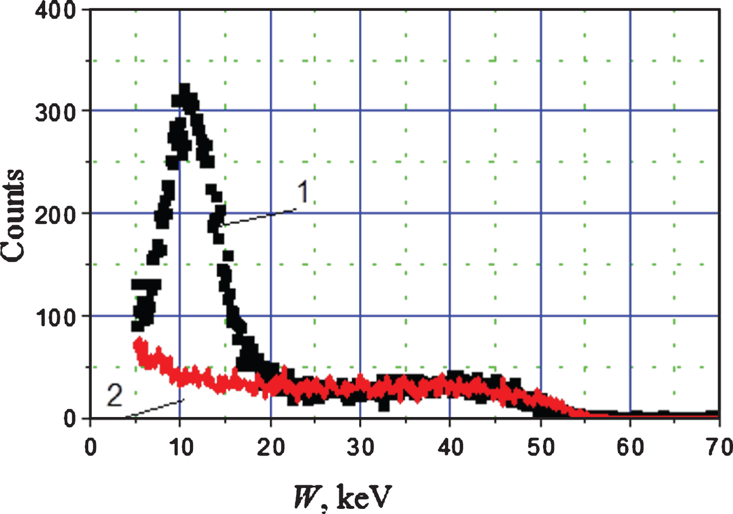
1) Amplitude spectra of a detector with planar electrodes for various voltage polarities: 1) photons impinge on the cathode, 2) photons impinge on the anode.
Figure 1 shows measurements made with a GaAs (Cr) detector for different voltage polarities. The detector with planar, square-shaped electrodes with a contact area of 0.1 cm2 and a thickness d = 400μm was mounted near γ-ray source. The irradiation was always carried out through the same electrode for different polarities of voltage. The orientation of the irradiation did not change. The bias polarity reversed. Bias voltage was 200 V. It can be seen that the spectra of the detectors with planar electrodes are missing the narrow peak of monoline 59.5 keV. Peak of monoline 17 keV occurs at only one polarity of applied bias voltage and it is shifted towards lower energies.
Based on the results of modelling the small pixel effect [18, 19], it can be asserted that the shape of the energy spectrum in the pixel detector should depend both on geometrical factors such as the sizes of the pixel contact and material parameters (τ n , τ p , μ p , μ n ), and on the average electric field within the detector. In order to optimize the characteristics of the spectrometric pixel detector, mathematical modelling must be done to find the shape of the amplitude spectrum of the detector, it is also important and to be able to do preliminary simplified calculations to find the shape of the energy spectrum. This is the goal of the present paper, which proposes a simple method for calculating the spectrumshape.
For the calculations we apply the following simplification. We assume that after the absorption of a photon at some point of depth z0, packets of electrons and holes are generated at this point and are immediately separated by the electric field [20] and drift along the electric field to the corresponding electrodes with velocities ν n μ n = μ n · E0, · ν p = μ p · E0, where E0 is the average electric field in the detector. Moreover, the coordinates of the packets of electrons and holes will vary with time t as follows: z n = z0 ± ν n t, · z p = z0 ± z p t (the sign is chosen depending on the direction of the electric field), here t is time.
We assume that the moving packets of electrons and holes are concentrated at geometric points (diffusion is neglected). We also assume that the potential is the same at all pixel contacts, the gaps between pixels are negligible and therefore the problem of the distribution of the electric field due to moving charges in the active region is reduced to the problem of charges moving in space between two infinite conducting plates [15]. Next, we consider the situation where the trajectory of the moving charges is on the axis passing through the centre of the pixel with coordinates x = 0and y = 0.
Due to the finite electron and hole lifetimes, the value of the charges in the packets will vary according to the following law: , here Q0 is the initial charge of holes or electrons that appear where a photon is absorbed. Meanwhile, the movement of electrons and holes that appear as a result of photon absorption generate an electric current in the active region of the detector and displacement currents will flow via pixel contacts [15]:
To find the electric field created by moving charges near the surface of the contacts of different pixels, we used the imaging method of [18]. In accordance with the imaging method, the distribution of the electric field near the metal contact plane is equivalent to the field created by an infinite series of positive and negative charges. The model for the calculation is shown schematically in Fig. 2. If the charge Q (dark circle) occurs in the detector, charges with both opposite (light circles) and similar (dark circles), signs appear beyond the electrode’s surface. When the charges move, their reflected charges also change coordinates. The expression for the excess of the electric field E (t, x, y) due to the charges in the active region in a plane z = d where pixel metal contacts are, is:
- distance from negative charge of image k, caused by packets of electrons in the detector, to the contact surface of the pixel.
- distance from negative charge of image k, caused by packets of holes, to the contact surface of the pixel.
- distance from positive charge of image k, caused by packets of holes, to the contact surface of the pixel (Fig. 2).
Expression (2) is valid when the cathode coordinate is zero and the pixel contacts are anodes. For the opposite case, when the coordinate of the anode is equal to zero, and pixel contacts are the cathodes in (2), the sign of vn and vp must be changed.
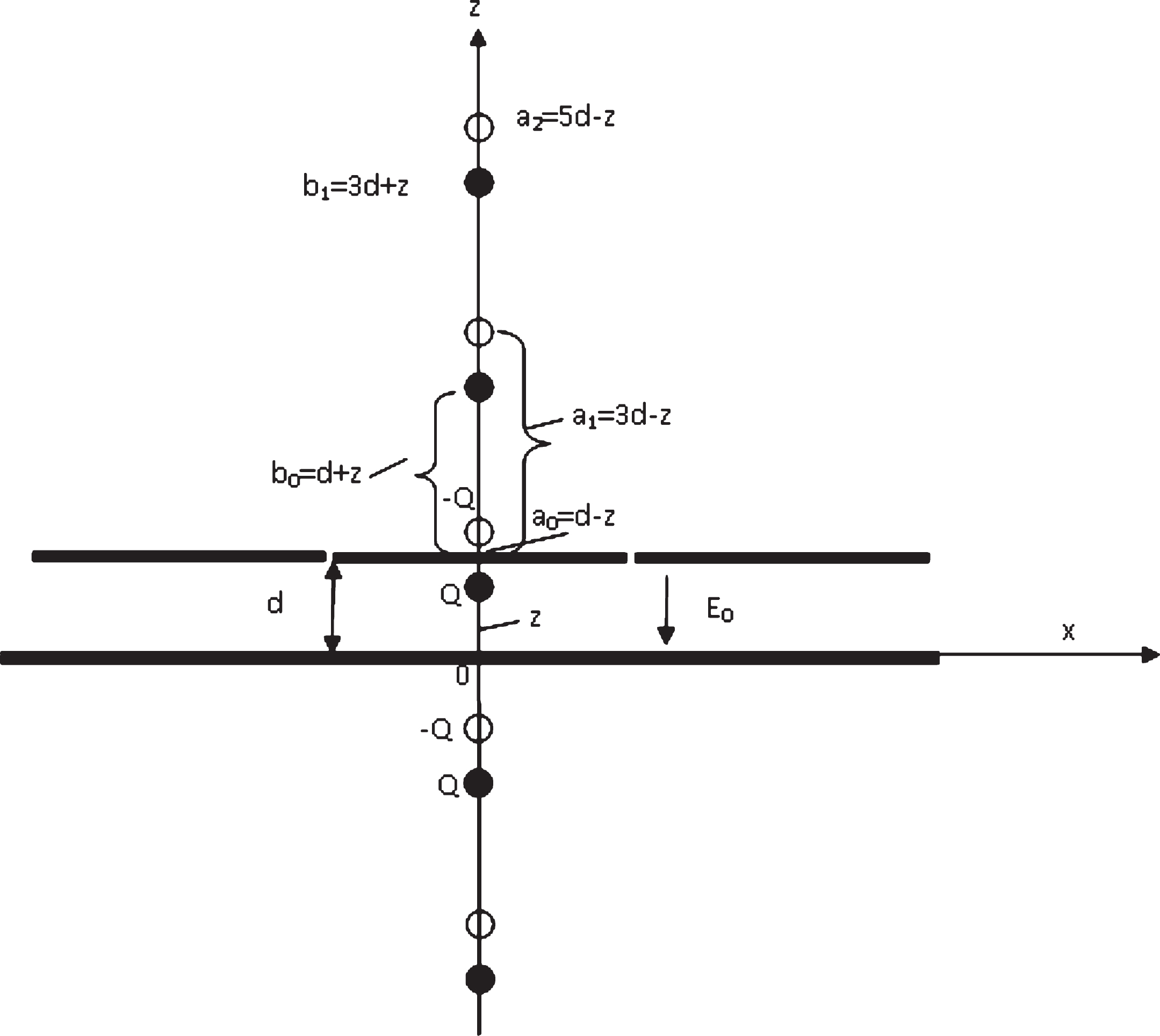
An image of the charges in a pixel detector.
Hybrid pixel detector includes semiconductor detector and readout chip. Medipix3 and Timepix are the last generations of a CMOS pixel detector readout chip. Both chips have a 256 by 256 matrix of 55μm square pixels. So it is interesting to determine parameters pixel detectors with pixel pitch 50 um. Calculations using (1) and (2) were done for a GaAs (Cr) pixel detector with a thickness of d = 500μm and pixel pitch of 50μm. The mobility of electrons and holes is assumed to be μn = 3000 cm2/Vs, μp = 300cm2/Vs, and lifetimes, respectively, were τ n = 20 ns, τ p = 1ns [21]. It was assumed that the trapped charges do not contribute to the change in the electric field, and the derivative is caused only by the movement of the charge. Calculations were performed for different polarities for the following average electric field intensities in the detector: E0 = 5 kV/cm. To conduct the experiments Mathcad 14.0, a powerful software which allows to calculate all formulas while doing the sum, was used.
Figure 3 shows the function of the current i0 over time flowing through the central pixel as a function of the depth coordinates of the photon absorption z0. The calculations given in Fig. 3 are for the case when the pixel contacts of the detector are anodes and the cathode coordinate is zero. From the relationship shown in the figures, it follows that the duration of the output pulse current in the pixel is determined only by the time of electron drift from the point z0 where the charge is generated. As the electrons drift to the anode, the current continuously increases and reaches a maximum when they reach the anode. The current increases due to the decrease in the distance between the electron packet and the conductive pixel contact, which rapidly increases the excess electric field. At the same time, an increasing number of flux lines close on a pixel area.
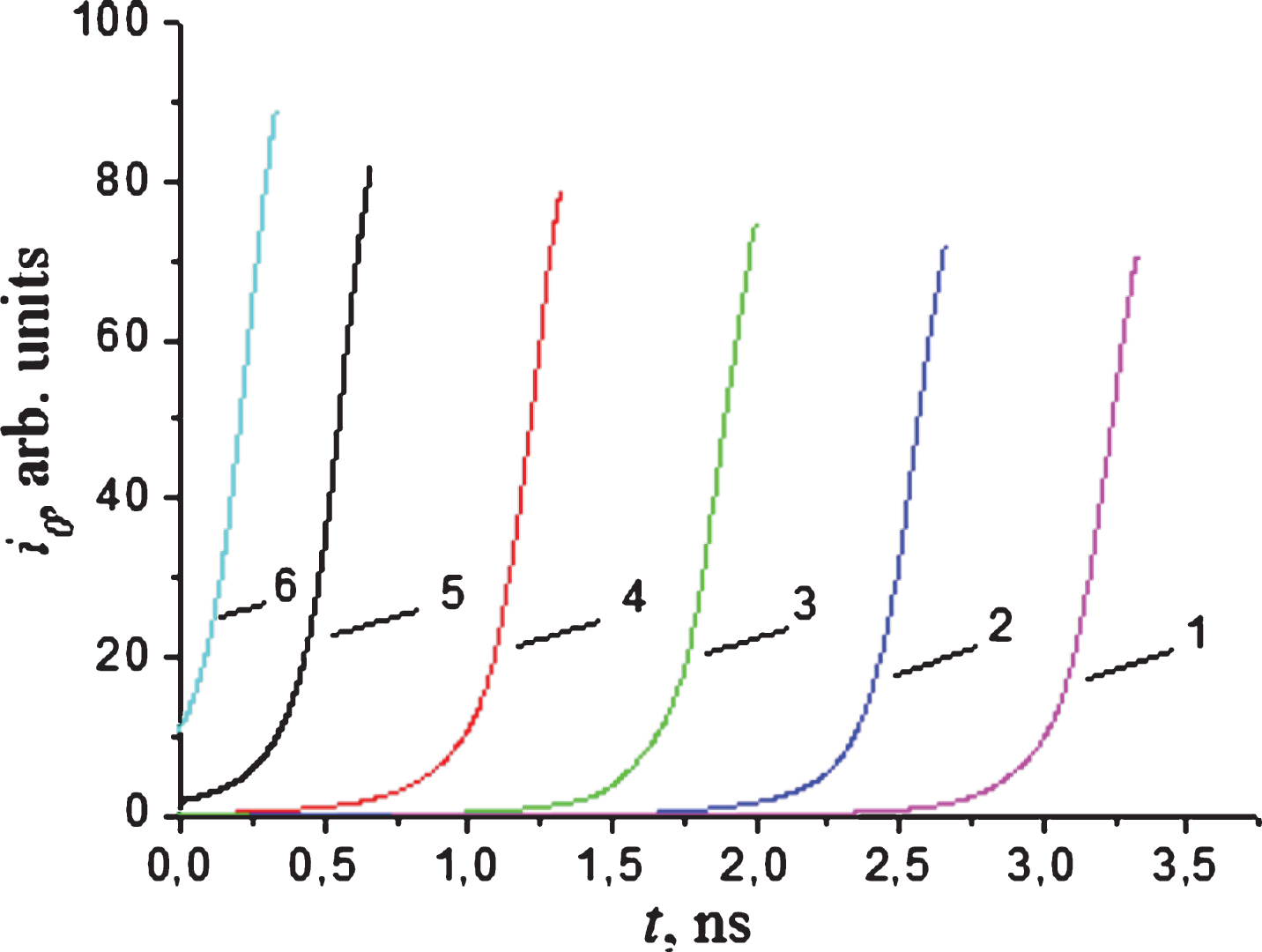
The function of the current in the pixel over time for different x-ray photon absorption coordinates z0 for E0 = 5 kV/cm (pixels are anodes). 1 – z0 = 0μm, 2 – z0 = 100μm, 3 – z0 = 200μm, 4 – z0 = 300μm, 5 – z0 = 400μm, 6 – z0 = 450μm.
A completely different situation occurs when polarity of the voltage at the detector is changed, as shown in Fig. 4. When the pixel is a cathode, observable currents flow through the pixel only when the charge of non-equilibrium carriers is generated near the pixel (400< z0<500μm). For all other points, the maximum currents are negligibly small. To find the charge Q collected at the pixel over the time the charges drift from the point with depth coordinate z0, the functions in Figs. 3 and 4 should be integrated over time. The values of the integrals ∫i D dt = Q normalized to Q0 are equal, by definition, to the charge collection efficiency (CCE), here Q is the charge collected at the electrode of the detector after the moving charges disappear from the active area of the detector.
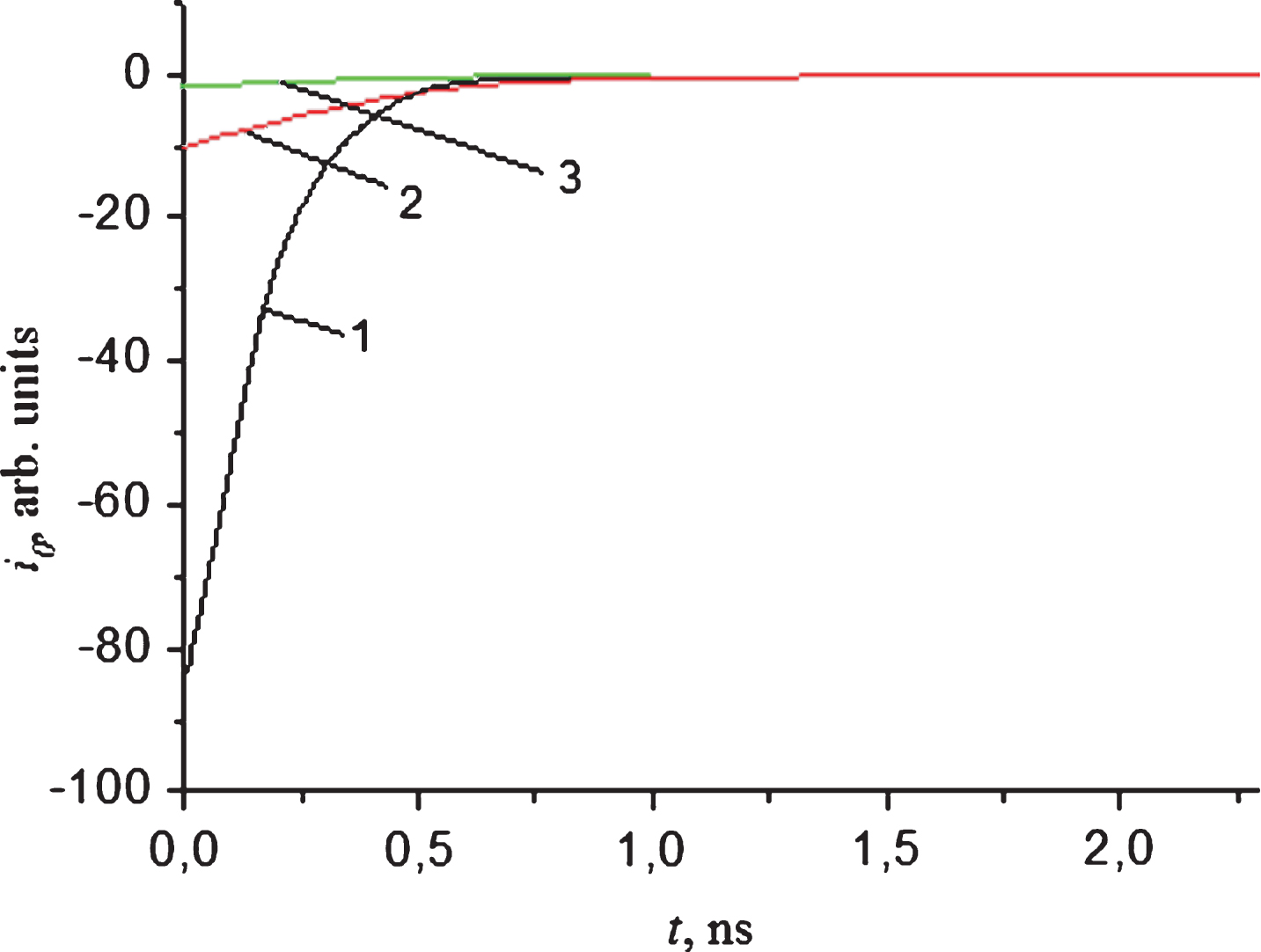
The function of the current through the pixel contact over time for different x-ray photon absorption coordinates for E0 = 5 kV/cm (pixels are cathodes). 1 – z0 = 500μm, 2 – z0 = 450μm, 3 – z0 = 400μm.
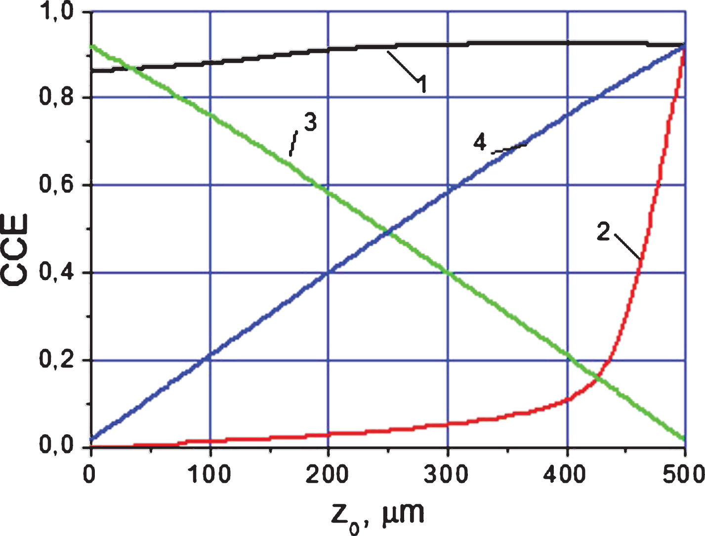
CCE(z0) for different detector: 1CCE(z0) for a pixel detector (pixel is anode); 2CCE(z0) for a pixel detector (pixel is cathode); 3- CCE(z0) for detector with planar electrodes (photons impinge on the detector cathode); 4-CCE(z0) for detector with planar electrodes (photons impinge on the detector anode).
These functions for different polarity of applied bias voltage are shown in Fig. 5. As follows from Fig. 5, the functions of CCE (z0) for pixel detectors (curves 1 and 2) are fundamentally different from the known functions for detectors with planar electrodes, also shown in Fig. 5 (curves 3 and 4). Curves 3 and 4 were found from the Hecht equation [22]:
z0 is the coordinate of the absorbed photon,. l p = μ p · τ p · E0 is the drift length of the holes, d is the thickness of the detector and l n = μ n · τ n · E0 is the drift length of the electrons.
Curves 1 and 3 were obtained, respectively, for pixel and detectors with planar electrodes for E0 = 5 kV/cm. While CCE(z0) in a detector with planar electrodes drops almost linearly from 0.9 to zero as the coordinates of the photon absorption are changed from zero to d = 500μm, CCE in a pixel detector continuously increases, reaching the limit close to one. This result gives insight into the reason the 59.5 keV peak of isotope 241Am can be observed in the pixel detector [10], but not in the detectors with planar electrodes.
To calculate the amplitude spectrum, we used the equation [23]:
where W is the energy of photons recorded by the detector, is the distribution of the number of the events for energies W, W0 is the photon energy, α(W0) is a linear attenuation coefficient depending on the photon energy. Value σ is the standard deviation of energy in the formula for Gaussian distribution theorem. σ usually depends on noises of electronic measuring equipment and also noises of detector [23]. For the equipment in the current paper σ ≈ 3keV.
The shapes of the amplitude spectra for photons with energy W0 = 60 and 17 keV was found for pixel detector with pith 50μm and detectors with planar electrodes. The following parameters for GaAs (Cr) detectors were used [24]: d = 500 μm, E0 = 5 kV/cm, linear attenuation coefficient equal α= 10.9 cm–1 for W = 60 keV and α= 351.8 cm–1 for 17 keV. The standard deviation of energy equal to 3 keV. Equation (4) was used for the calculations, taking the functions of CCE(z0) for the pixel detector shown in Fig. 5. For detectors with planar electrodes CCE(z0) was found from the Hecht equation [22]. The behaviour of CCE(z0) was approximated by a second-order polynomial CCE(z) = 0.85+3.4×10⁻⁴z-4.2×10⁻⁷z2 for curve 1 (Fig. 5). Exponential function for curves 2 is: CCE = 2.5×10⁻⁵exp(z/48).
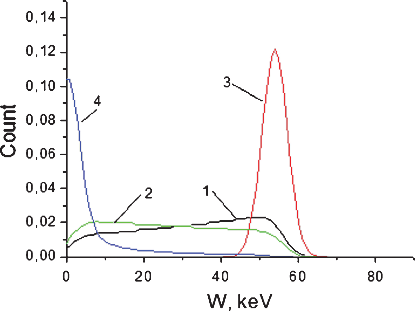
The shape of the amplitude spectra for W0 = 60 keV: 1- Photons impinge on the cathode of detector with planar electrodes (curve1); 2- Photons impinge on the anode of detector with planar electrodes (curve 2); 3- Pixels are anodes, photons impinge on the cathode of the pixel detector (curve 3); 4- Pixels are cathodes, photons impinge on the anode of the pixel detector (curve 4).

The shape of the amplitude spectra for W0 = 17 keV: 1- Photons impinge on the cathode of detector with planar electrodes (curve 1); 2- Photons impinge on the anode of detector with planar electrodes (curve 2); 3- Pixels are anodes, photons impinge on the cathode of the pixel detector (curve 3); 4- Pixels are cathodes, photons impinge on the anode of the pixel detector (curve 4).
The results given in Figs. 6 and 7 show the shape of the amplitude spectra for W0 = 60 and 17 keV for different cases, which include following: Photons impinge on the cathode of detector with planar electrodes (curve1), Photons impinge on the anode of detector with planar electrodes (curve1), Pixels are anodes, photons impinge on the cathode of the pixel detector (curve3), Pixels are cathodes, photons impinge on the anode of the pixel detector (curve 4),
The amplitude spectrum of the detector with planar electrodes (curves 1 and 2 in Fig. 6) has no peaks at energy of W0 = 60 keV. This is caused by two reasons: short lifetime of holes t p and small linear attenuation coefficient at an energy of 60 keV. So, only electrons are collected by the detector anode and CCE is a function from the point of photon absorption z0 as shown in Fig. 5 (curve3). Thus, collected charge depends on the photon absorption coordinate. But at value α = 10.9 cm–1 with energy W0 = 60 keV, X-ray quantum are absorbed almost evenly in an active field of the detector. Therefore, the spectrum has similar values in the energy range from 0 to 60 keV at different polarities of applied bias voltage. Calculated spectra are consistent with the ones obtained experimentally in GaAs (Cr) detectors (Fig. 1, curves1 and 2).
Other functions were obtained for pixel detectors. The amplitude spectrum of the pixel detector contains a sharp peak (FWHM = 8 keV) corresponding to photons with an energy of 60 keV, taking the functions of CCE(z0) for pixels which are anodes (Fig. 5). In the case where pixels are cathodes, the peak is shifted towards lower energies with values no more than 10 keV.
Due to high value of linear attenuation coefficient at energy of 17 keV almost all photons are absorbed in gallium arsenide at a depth of 20–30μm. If photons are absorbed on the cathode, the CCE value is almost equal to 1 and electrons are collected on the anode. In this case spectra in pixel detectors and in a detector with planar electrodes have narrow sharp peak corresponding to 17 keV(FWHM = 8 keV).
In addition, one more characteristic of pixel detectors must be mentioned. Figure 8 depicts a way of calculating pixel detectors where the pixel is the anode and the photon is absorbed at a depth of 250μm. Current-time functions in the central pixel and summed current of four pixels which surround it are shown in Fig. 8. Calculations show that, while the current increases rapidly at the central pixel, the current may either decrease or change signs in the adjacent pixels. It is evident that at a certain time the total current in the four adjacent pixels is negative.
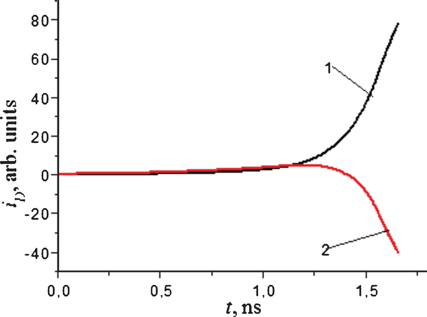
The function of current over time in the central pixel (1) and in four adjacent contacts (2). (z 0 = 250μm, E 0 = 5 kV/cm).
The difference in shapes of dependences of currents in central and neighboring pixels is caused by the following factors. Movement of electrons towards the anode in the central pixel leads to a constant intensification of the electric field. At the same time, normal component of the electric field in the neighboring pixel starts to decrease at some point causing negative polarity of current in these pixels. Change of normal components of the electric field in central and neighboring pixels at different time t1 and t2 is shown schematically in Fig. 9. That effect might be an explanation for difference of dependences CCE (z0) existed in pixel detectors and detectors with planar electrodes (Fig. 5, curves1 and 3).
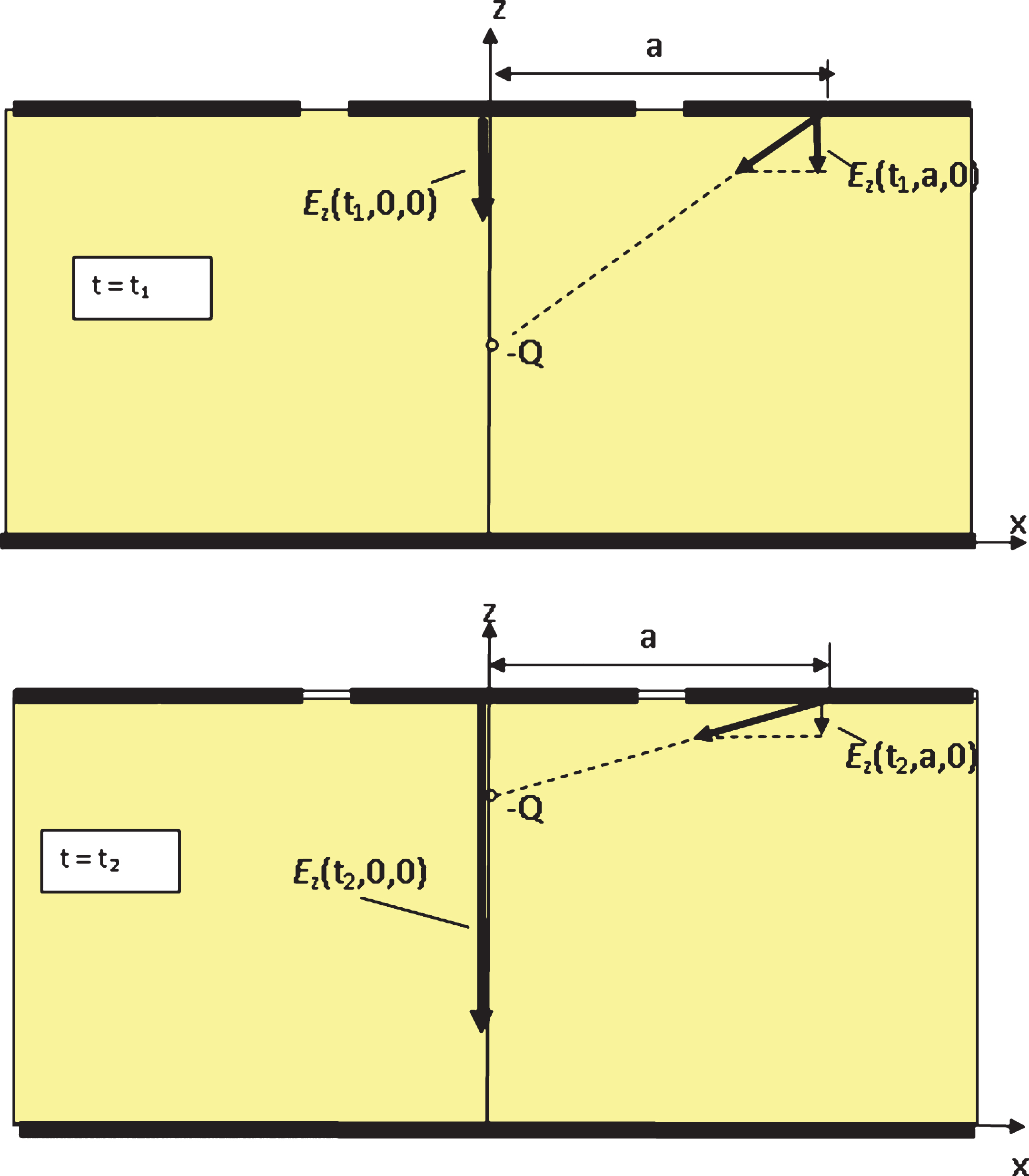
Schematic image of change of normal electric field components in central and neighboring pixels at different time t1 and t2 caused by packet of electrons moving toward pixels.
The amplitude spectra of a pixel X-ray detector were calculated using a simple physical model. The calculation results are in qualitative agreement with the experimental data [10]. It is shown that in a pixel detector, where μ n · τ n >> μ p · τ, amplitude spectra with high energy resolution can be obtained. This is because the signal is taken from the contact of just one pixel, where the function of the current over time is very different from the same function at adjacent pixel contacts. Moreover, such properties can be observed only under the condition that the pixel contact receives voltage with positive polarity.
The results can be useful for finding the amplitude spectra of X-ray pixel detectors made from CdTe or Se. This calculation method can be improved. For a detailed calculation of the shape of the amplitude spectrum, the variations of CCE for charges whose trajectories cross the whole area of the pixel contact must be taken into consideration. Equation (2) can be used for such calculations.