




Abstract
With the popularity of portable electronic devices, the demand for 12-bit low-power analog-to-digital converter (ADC) chips continues to grow. Considering that these devices typically rely on battery power, high precision and stability are crucial. In order to improve the voltage resistance of ADC chips under high voltage, an innovative bootstrap sampling switch design is proposed, which utilizes the capacitance characteristics of NMOS and PMOS transistors to enhance the voltage resistance of the chip. At the same time, considering factors such as power fluctuations, time domain and voltage interleaving, a two-stage hybrid architecture based on successive approximation registers (SARs) and time to digital converters (TDCs) was studied and designed to optimize the balance between low power consumption and high voltage resistance performance. The results showed that the power consumption of the chip design was only 9.5 mW. The voltage compensation measures significantly reduced the error value from 7.01% to 1.97%, optimizing 5.04%. In summary, this design not only improves the accuracy and speed of ADC chips, but also successfully controls the exponential growth of power consumption, which has strong practical value. The proposed solution by the research institute has broad potential in multiple application fields, especially suitable for situations with high requirements for power consumption and stability, such as medical imaging and aerospace. This design provides new ideas and directions for the development of high-performance and low-power ADC chips in the future.
Introduction
In today’s electronic systems, analog-to-digital converters (ADCs) play an indispensable role, especially in the fields of precision measurement and portable devices. 1 Among them, 12-bit low-power ADC chips are highly favored due to their excellent accuracy and energy-saving characteristics. This type of ADC chip is widely used in fields such as healthcare, environmental monitoring, portable instruments, and industrial control systems. 2 However, in practical applications, ADC chips face many challenges, especially the impact of voltage fluctuations on chip performance. Due to external factors such as power fluctuations, temperature changes, and signal interference, existing ADC designs often struggle to ensure stable performance in these unstable voltage environments, resulting in decreased accuracy and increased power consumption. In response to this issue, an innovative bootstrap sampling switch design has been proposed, aiming to significantly improve the voltage resistance performance of 12-bit low-power ADC chips under high voltage, while optimizing power consumption and accuracy. Therefore, evaluating the withstand voltage performance of ADC chips is crucial to ensure their reliability and stability under various working conditions. Voltage resistance refers to the maximum voltage that electronic components can safely withstand without damage. 3 For low-power ADC chips, superior withstand voltage performance can not only improve product safety and reduce failure rates, but also extend product lifespan, especially in voltage unstable environments. With the development of technology, the sampling rate of 12-bit resolution ADC chips has been increased to 18 Gb/s. 4 When the sampling phase is constant, the higher the single-phase sampling speed and accuracy, the higher the accuracy and speed of the time-domain and voltage interleaved ADC chip. 5 But its power consumption will show exponential growth with the increase of sampling bits and speed. Therefore, in this context, research is dedicated to designing an ADC chip that combines low power consumption and high voltage resistance. To this end, an innovative ADC chip design based on a two-level hybrid architecture of successive approximation register (SAR) and time to digital converter (TDC) was proposed to enhance the performance stability of low-power ADC chips in unstable voltage environments. The contribution of the research lies in providing a high voltage resistance, low power consumption, and high-precision ADC chip design scheme for future portable electronic devices, especially suitable for applications with strict requirements for power consumption and stability.
The research content includes four parts. The second part is a review of the current research status of ADC chips and SAR-ADC chips both domestically and internationally. The third part is the design of a 12-bit low-power two-level hybrid architecture ADC chip circuit. The first section conducts research on the ADC chip architecture based on SAR-TDC, and the second section conducts low-power circuit design for a 12-bit resolution ADC chip. The fourth part is the simulation verification of a 12-bit low-power two-level hybrid architecture ADC chip circuit.
Related works
ADC chips can convert analog signals into digital form for electronic devices to process and analyze, so they have received widespread attention in many fields, and many researchers have conducted in-depth research on them. Researchers such as Pazhouhandeh M R proposed a 32 channel bidirectional CMOS neural interface to achieve efficient treatment of neurological diseases. Each channel of this design contains a neural ADC, and the effectiveness of this method was demonstrated through whole brain validation in rodents. 6 To address the challenges of high-performance analog integrated circuit design in nanoscale CMOS technology, Gielen GGE et al. proposed a time coding based ADC method. This method used ADC technology of voltage controlled oscillators to achieve the functions of analog circuits in a highly digitized form. The results showed that this method was feasible in addressing the challenges of nanoscale CMOS technology. 7 To minimize the power consumption and cost of ADC, Mulleti S and other scholars proposed a prototype design of modular computing hardware, which adopted modular folding technology to avoid signal clipping. In addition, to fold signals with higher frequencies than existing hardware, modular hardware operated before sampling. The results showed that this method effectively reduced the power consumption and cost of ADC. 8
The SAR-ADC chip stands out among numerous ADC chips due to its advantages of low power consumption and medium to high precision, becoming a current research hotspot. To improve the efficiency and energy-saving performance of ADCs, Yi P’s research team proposed a compact noise shaping SAR-ADC based on error feedback structure. This method used a unit gain buffer and a ping-pong operation delay element to replace the traditional cascaded integrator feedforward structure for error feedback. The results showed that the design achieved a signal to noise ratio (SNR) and signal to noise distortion ratio (SNDR) of 79.3 dB at 16 times oversampling ratio. 9 Miki T and other scholars proposed a method called “random interrupt jitter technique” to enhance the defense ability of SAR-ADC against bypass attacks. This technology reduced the correlation between the analog input and the reference charge flow by introducing a significant jitter in the analog input, which was equivalent to a quarter of the full scale of the ADC. The results showed that compared to traditional reference charge bypass attacks on SCA, this innovative tamper proof ADC could reduce information leakage to 0.8 bits. 10 Tang X et al. proposed a second-order noise shaping technique with a closed-loop dynamic amplifier to enhance the energy efficiency of SAR-ADC in the face of process, voltage, and temperature changes. This technology adopted a closed-loop structure and dynamic operation, embedding a closed-loop dynamic amplifier into a loop filter designed for second-order noise shaping SAR. The results showed that this method effectively improved the energy efficiency of SAR-ADC. 11
Summary of literature review.
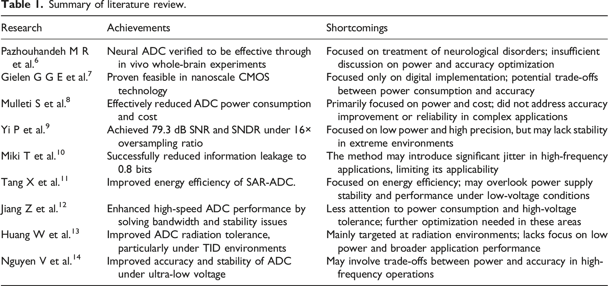
In summary, many existing ADC designs, such as the noise shaping SAR-ADC proposed by Yi P and the second-order noise shaping design proposed by Tang X, have not fully focused on stability and high reliability at extremely low voltages while pursuing high energy efficiency and accuracy. Moreover, under high-frequency operation, these designs may face additional power consumption and accuracy losses. In addition, although Nguyen V et al.'s ultra-low voltage FDC design solves the variability problem under low voltage, power consumption and stability issues still exist under high-frequency operation. In response to the above limitations, an innovative ADC chip design scheme with high voltage resistance, low power consumption, and high precision has been developed. Leverage the capacitance properties of NMOS and PMOS transistors to enhance the voltage tolerance of the chip, thereby offering device manufacturers more stable and reliable products.
Circuit design of a two-level hybrid architecture ADC chip with 12-bit low power consumption
This chapter explores the basic architecture of SAR-ADC chips and analyzes the quantization process of ADC chips based on SAR-TDC, revealing their innovative applications in time coding and digital conversion. Research on ADC chips based on SAR-TDC is expected to provide new basis for mixed signal integrated circuit design and a new perspective for efficient ADC implementation.
ADC chip based on SAR-TDC
SAR is a technique used for ADC, which allows for the conversion of analog signals into digital signals through a stepwise approximation method.
15
SAR-ADC is an efficient, precise, and widely used converter for low-power and medium speed applications. Due to its stepwise approximation method, SAR-ADC does not require continuous comparison operations, which often leads to lower power consumption. Compared with other types of ADCs, the design of SAR-ADC is relatively simple because it does not require complex clock management or high-speed operational amplifiers. The basic architecture of the SAR-ADC chip is shown in Figure 1. The basic architecture of SAR-ADC chip.
As shown in Figure 1, SAR-ADC mainly consists of sample and hold (S/H) circuit, digital to analog converter (DAC), comparator, SAR, and TDC. SAR is responsible for generating digital outputs, while DAC converts these digital values into analog signals for comparison. The comparator determines the size relationship between the input signal and the DAC output, while the timing controller ensures that the data conversion process proceeds in an orderly manner. The evaluation indicators for ADC performance include static and dynamic characteristics. The static characteristics focus on the performance of the device in steady-state, while the dynamic characteristics describe the performance when the input signal changes dynamically.
16
Resolution, bias error, signal-to-noise ratio, and sampling rate are key indicators for evaluating ADC performance.
17
The resolution of ADC refers to its ability to recognize and convert the minimum amount of variation in the input signal.
18
In the digital field, resolution is usually expressed as the number of bits that ADC can convert. In the field of simulation, resolution refers to the minimum input voltage change that the ADC can detect.
19
The mathematical expression for resolution is shown in equation (1).
In equation (1), 
In equation (2), 
In equation (3), 
In equation (4), 
In equation (5), The quantization process of ADC chip based on SAR-TDC.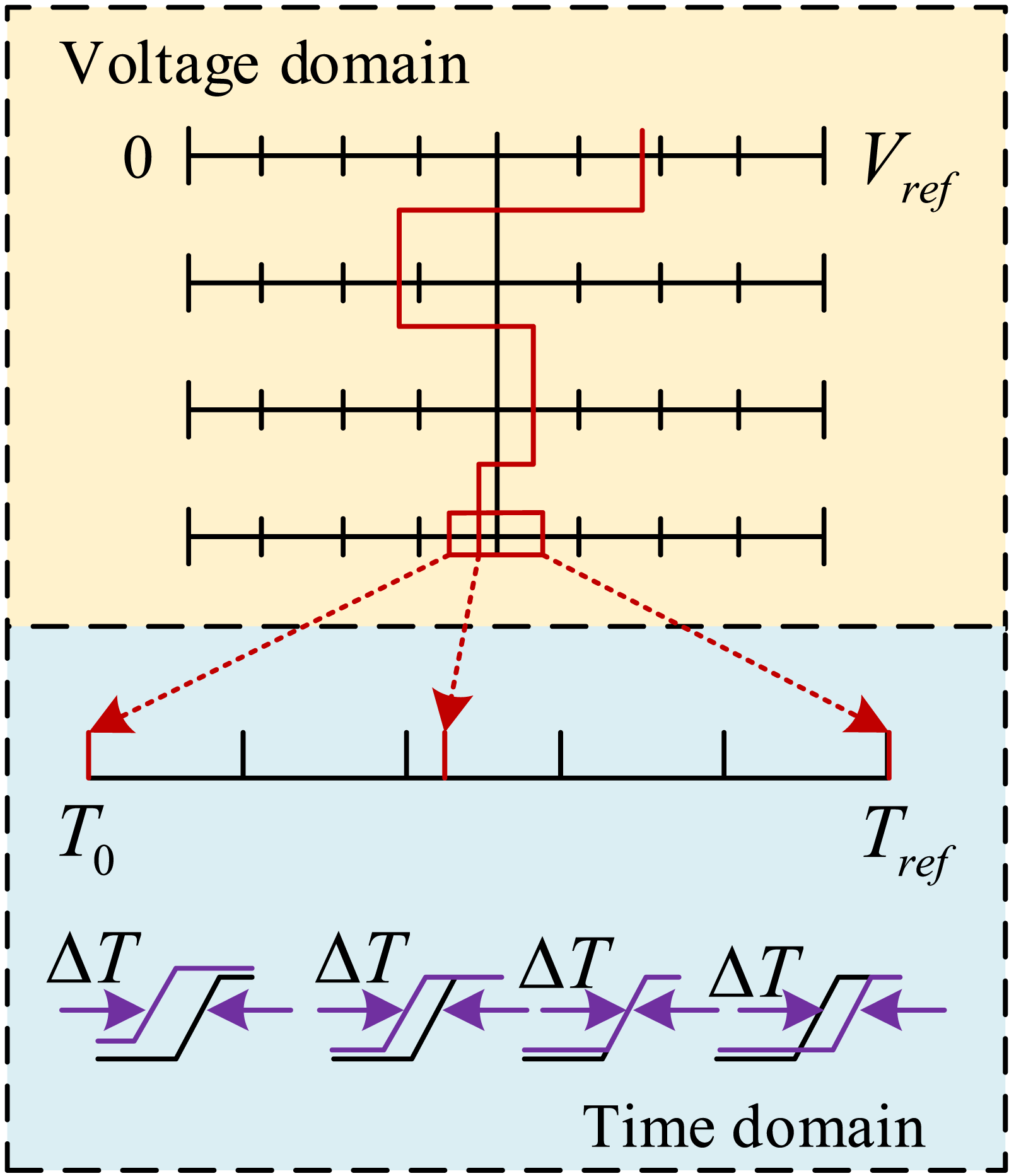
As shown in Figure 2, the quantization process in the SAR-TDC hybrid ADC chip is performed as a reference voltage, with the quantization range of SAR-ADC ranging from 0 to
Low-power circuit design of ADC based on 12-bit resolution SAR-TDC
When exploring ADC chips based on SAR-TDC architecture in depth, a signal acquisition and conversion mechanism combining the high-speed operation characteristics of TDC with the low energy consumption advantages of SAR was proposed. Aiming at the dual requirements of low power consumption and high voltage resistance, an ADC circuit based on 12-bit resolution SAR-TDC was studied and designed. In the circuit design process, optimization strategies such as dynamic residual amplification and bootstrap sampling switches were adopted to reduce power consumption while improving conversion rate and dynamic performance. The hybrid architecture based on SAR-TDC adopts a two-stage design. In the first stage, the SAR module is used to roughly approximate the input signal, while in the second stage, the TDC module is used to accurately measure the approximated signal. The innovation of this design architecture lies in the use of a bootstrap sampling switch design based on the capacitance characteristics of NMOS and PMOS transistors to enhance the stability of the chip in high voltage environments. This design effectively reduces errors caused by voltage fluctuations and ensures higher accuracy during the sampling process. In addition, the study also utilizes dynamic residual amplification technology to dynamically amplify signal residuals, in order to further improve the linearity and signal-to-noise ratio of the system, thereby optimizing performance under low power consumption. The low-power ADC circuit based on 12-bit resolution SAR-TDC is shown in Figure 3. Low-power ADC circuit based on 12-bit resolution SAR-TDC.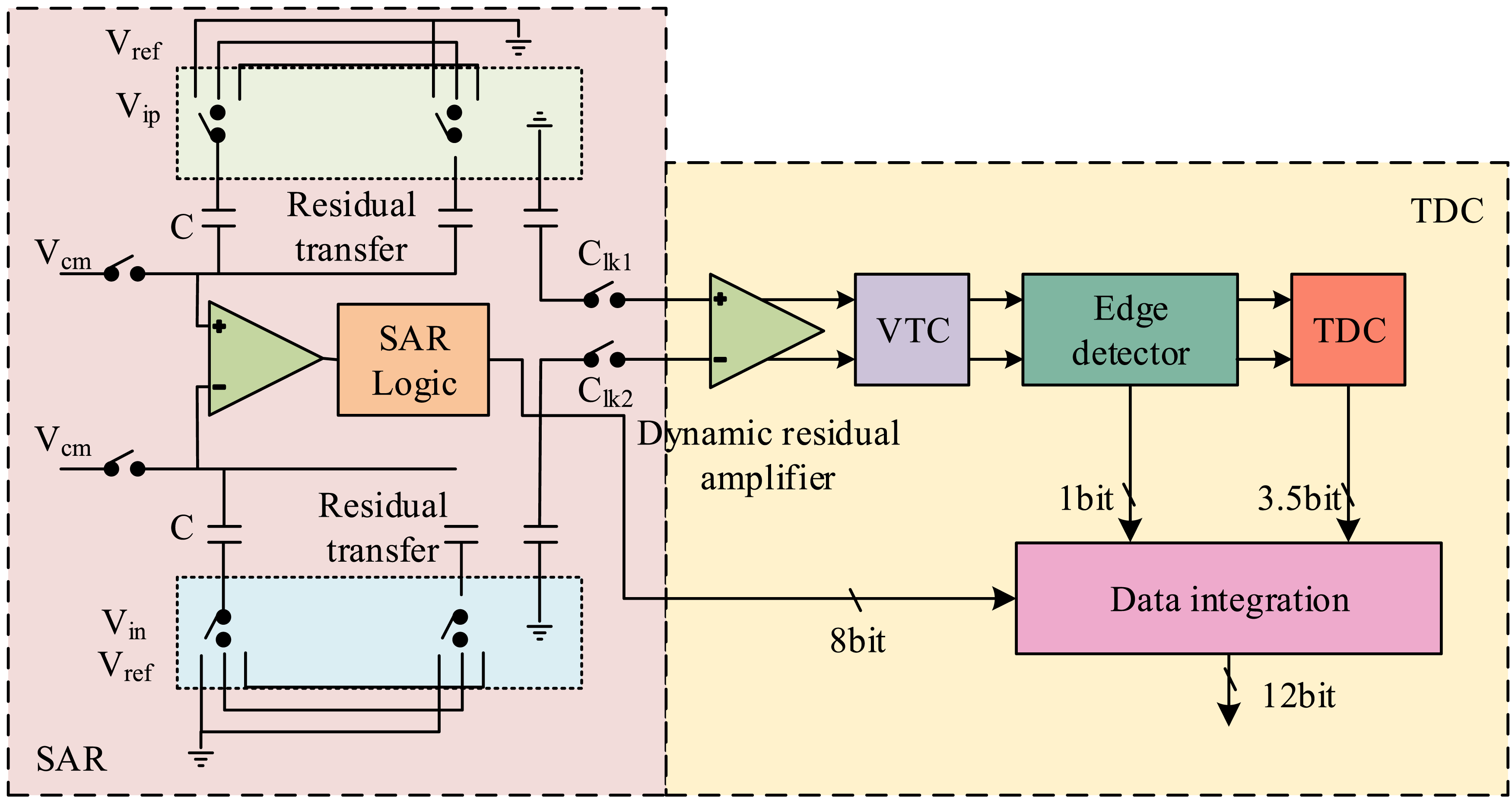
As shown in Figure 3, in the low-power circuit design of SAR-TDC hybrid ADC based on 12-bit resolution, an 8-bit resolution SAR-ADC architecture and a 4.5-bit resolution TDC-ADC architecture are integrated, with a 0.5-bit resolution used as redundant bits to improve the robustness of the system. This design also integrates a data fusion module and a residual transfer module to optimize data processing and accuracy during the conversion process. Among them, the SAR-ADC part includes a comparator, sampling switch, logic control circuit, and a binary capacitor array, responsible for preliminary ADC. In the integration part of TDC-ADC, the system adopts VTC, edge detector, TDC, and a dynamic residual amplifier to achieve finer conversion accuracy. The design of the dynamic residual amplifier considers the compensation mechanism for power supply fluctuations and temperature drift, and is manufactured using a 40 nm complementary metal oxide semiconductor process. In terms of power supply design, SAR-ADC and dynamic residual amplifiers use a 1.1 V power supply, while other components use a 0.8 V low voltage power supply. This layered power strategy helps to reduce overall power consumption, ensuring system energy efficiency and performance.
22
The binary capacitor array of SAR-ADC is shown in Figure 4. Binary capacitive array of SAR-ADC.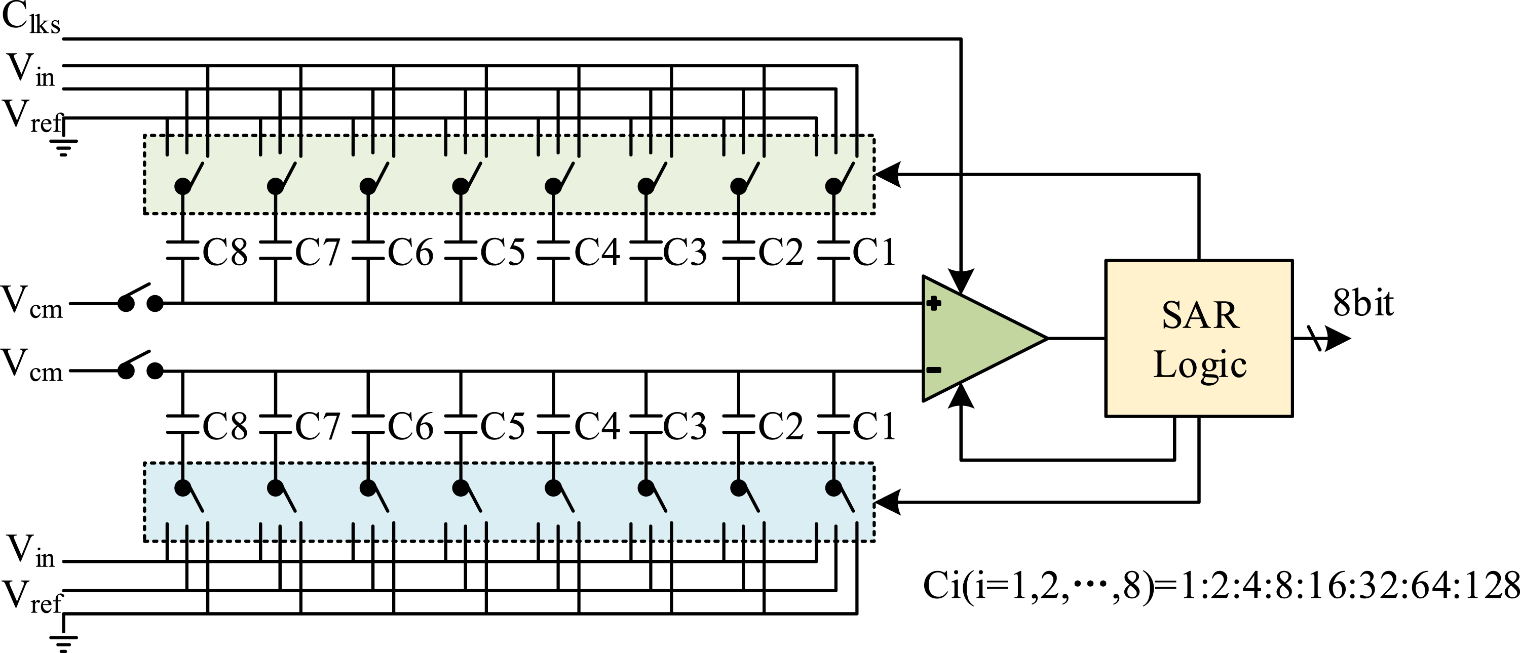
As shown in Figure 4, the SAR-ADC section uses a binary capacitor array consisting of 8 capacitor units labeled C1 to C8. Their capacitance values are set to (1, 2, 4, 8, 16, 32, 64, 128) times the reference capacitance C, forming an accurate binary weighted array for precise charge allocation and adjustment of the input signal during ADC. In terms of differential input, 
In equation (6), 
In equation (7), 
In equation (8), 
In equation (9), 
In equation (10), 
In equation (11), 
In equation (12), 
In equation (13), 
In equation (14), 
MOSFETs, especially NMOS transistors, are widely used as sampling switches due to their fast switching performance and small size. These switches utilize the conduction capability of MOSFETs, allowing the circuit to accurately sample analog signals based on the frequency of the clock signal. However, the conduction resistance of MOSFETs is not fixed and will change with time, especially when the value of Circuit design of bootstrap sampling switch.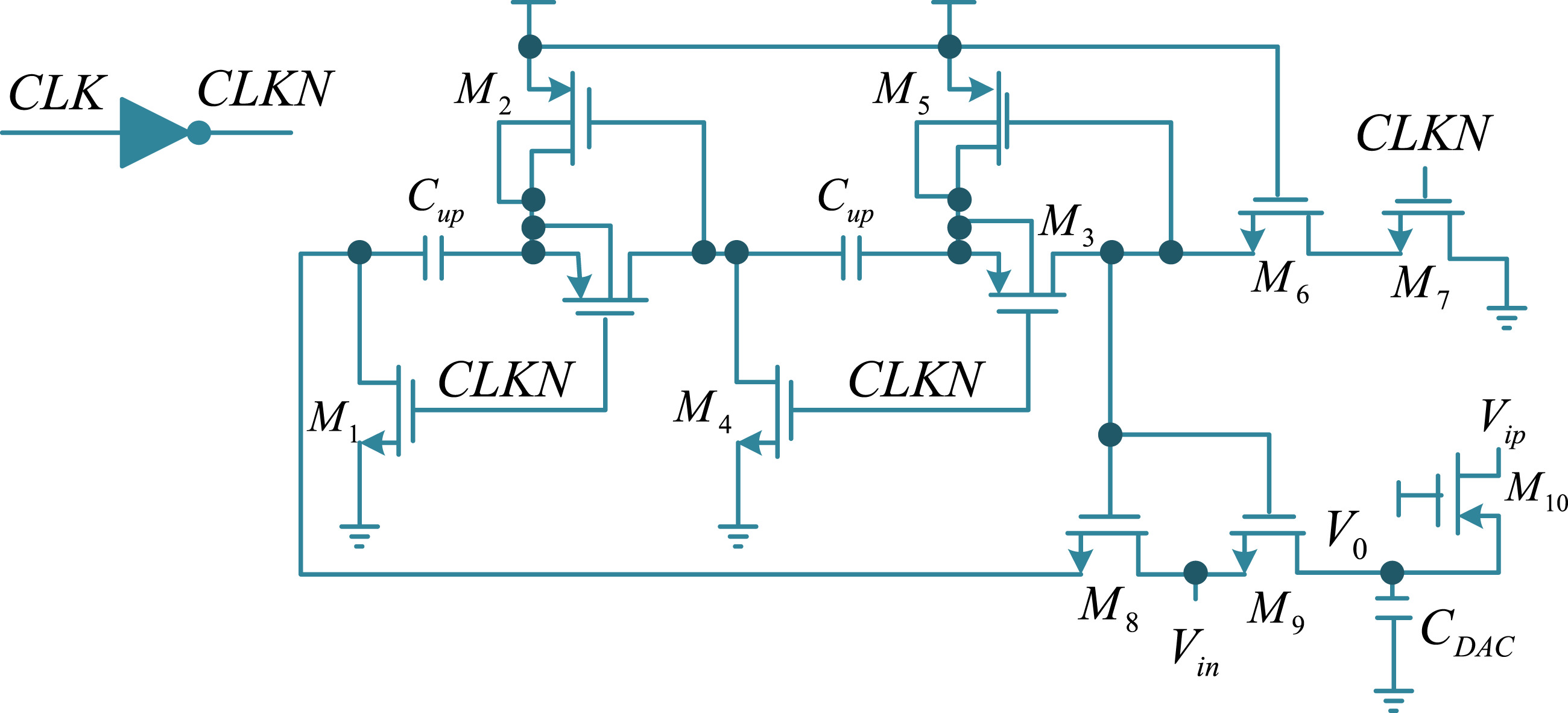
As shown in Figure 5, in the circuit design of the bootstrap sampling switch,
In order to improve the stability and reliability of ADC chips in practical applications, a detailed design of voltage compensation and temperature compensation mechanisms was studied, and optimization was carried out based on the working principle of bootstrap sampling switches. In addition, in the implementation of compensation algorithms, a new compensation algorithm framework was proposed by combining error feedback structures with temperature and voltage compensation models. This algorithm utilizes polynomial fitting method to model the voltage and temperature changes under different working environments, ensuring the effectiveness and adaptability of the compensation mechanism. The voltage compensation model is shown in equation (16).
In equation (16), 
In equation (17),
Simulation verification of a 12-bit low-power two-level hybrid architecture ADC chip circuit
This chapter first set up a simulation experimental environment, and then simulated the circuit of the ADC chip to further verify its resistance voltage performance. Through simulation experiments, the performance of the ADC chip was comprehensively evaluated, providing reliable basis for subsequent practical applications.
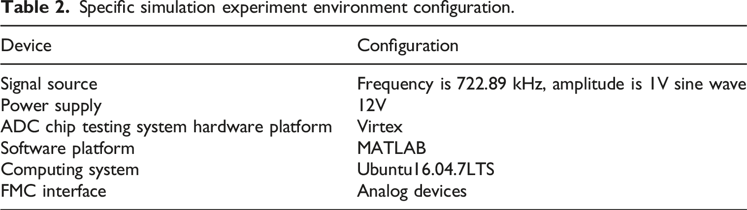
Experimental environment construction
Specific simulation experiment environment configuration.
ADC chip circuit simulation results
The study conducted simulation tests on ADC chips using the SPICE simulation platform, and the simulation results of the ADC chips are shown in Figure 6. SNR reflects the energy ratio between the input signal and noise, and a higher SNR indicates that the analog signal is less affected by noise during the conversion process. SDR measures how much original signal components are retained in the output signal while suppressing how much nonlinear distortion is present. A higher SDR means that the ADC performs well in maintaining signal fidelity. THD represents the intensity of harmonic interference caused by nonlinear components during ADC conversion, with higher values indicating a more linear system and smaller harmonics. SNDR is a comprehensive indicator of SNR and SDR, which represents the overall cleanliness of the system and is suitable for measuring the overall system quality of ADC. ENOB measures the true resolution of ADC in practical operation, and the closer it is to the ideal 12-bit resolution, the closer the design is to the theoretical limit. As can be seen from Figure 6, the SNR reached 65.1 dB, indicating that there was only a small amount of noise in the signal, and the signal to distortion ratio (SDR) was 74.4 dB, indicating a high purity and low distortion of the signal. SNDR and total harmonic distortion (THD) were 64.9 dB and 78.3 dB, respectively, further emphasizing signal quality. The effective number of bits (ENOB) was 10.19 bits, indicating a high quantization accuracy of ADC. Therefore, all indicators of the ADC chip met the reading requirements of the chip. ADC chip simulation results.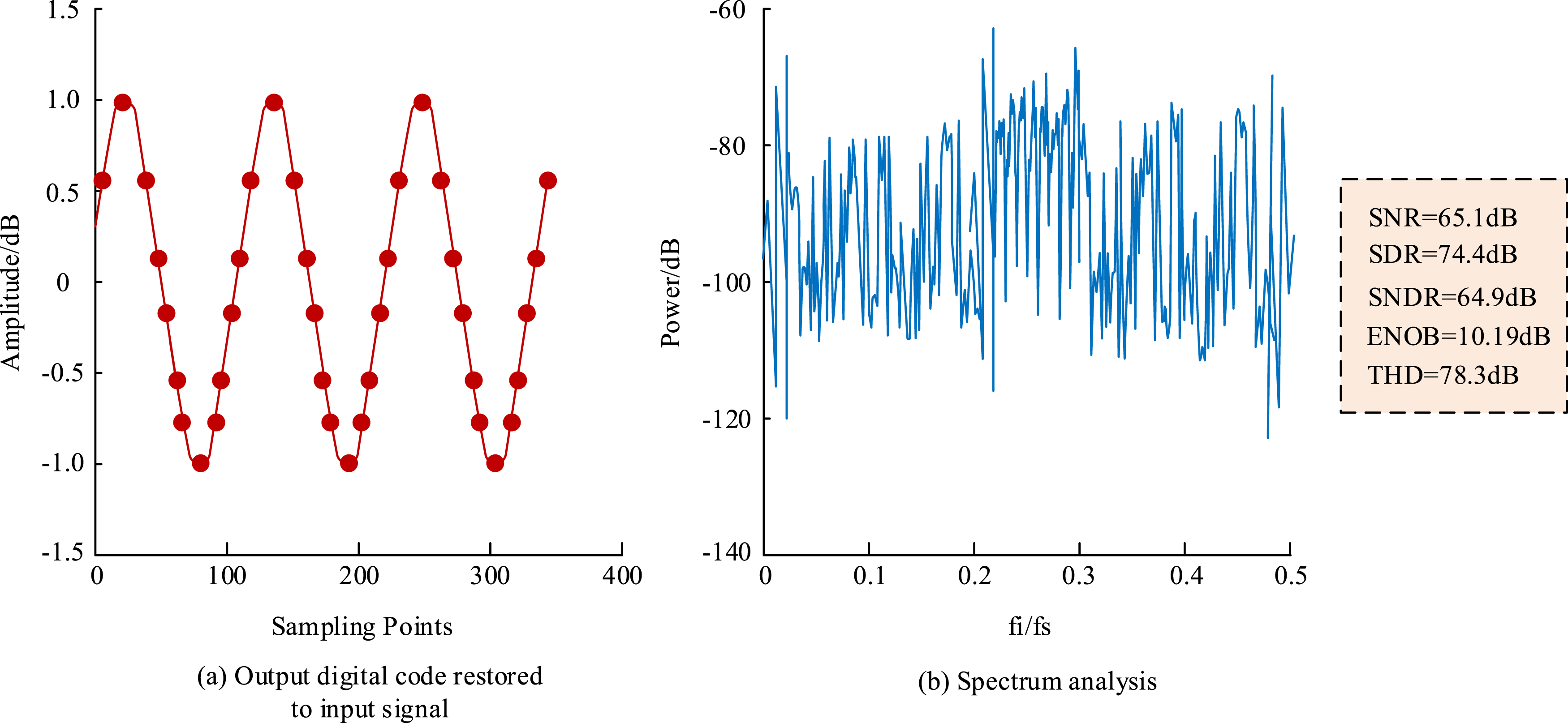
To further verify the accuracy of the ADC chip’s digital conversion output, the study connected it to two inverters and conducted transient simulation analysis. In the simulation test, the sampling frequency was set to 50 MS/s and the transient simulation time was 10 ms. The transient simulation diagram of the ADC chip is shown in Figure 7. From Figure 7, the transient simulation output of the ADC chip presented a sinusoidal signal waveform. This result indicated that the ADC chip successfully completed digital conversion output and its functional performance was accurate and error free. Transient simulation diagram of ADC chip.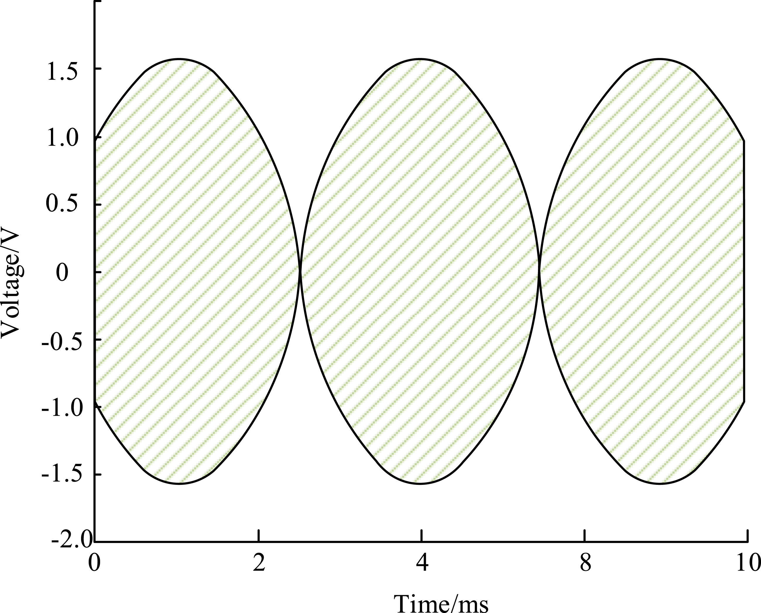
Simulation of voltage resistance performance of ADC chips
To verify the reliability and stability of ADC chips under various working conditions, a series of simulation tests were conducted to evaluate the gain performance of dynamic residual amplifiers under different temperature and power supply voltage conditions after implementing power fluctuation and temperature drift compensation mechanisms. The gain of the ADC chip after compensation under different working conditions is shown in Figure 8. From Figure 8(a), at a power supply voltage of 1.06 V, the chip achieved a maximum gain of 10.18 dB, while at 1.20 V, the gain slightly decreased, achieving a minimum gain of 9.95 dB. This change indicated that although the power supply voltage fluctuated, the compensation mechanism successfully limited the range of gain variation, ensuring the coherence and consistency of the chip output. From Figure 8(b), the ADC chip achieved a maximum gain of 10.20 dB at extreme low temperatures of −40°C, while the gain slightly decreased to 10.04 dB when the temperature increased to −10°C. Under different temperature conditions, the fluctuation of gain was controlled within a small range, demonstrating the excellent temperature adaptability and stable gain performance of ADC chips. In summary, with compensation mechanism, ADC chips could maintain the stability and reliability of their gain performance in the face of challenges such as power supply voltage fluctuations and temperature drift. In addition, the compensated gain stability ensures that the ADC can maintain consistent voltage conversion characteristics even under power supply fluctuations and temperature changes. Especially in outdoor or high-temperature industrial environments, this robustness is crucial for the long-term operation of the system. Gain of ADC chip after compensation under different working conditions. (a) Gain of ADC chip after compensation under different power supply voltages and (b) gain before and after compensation at different temperatures.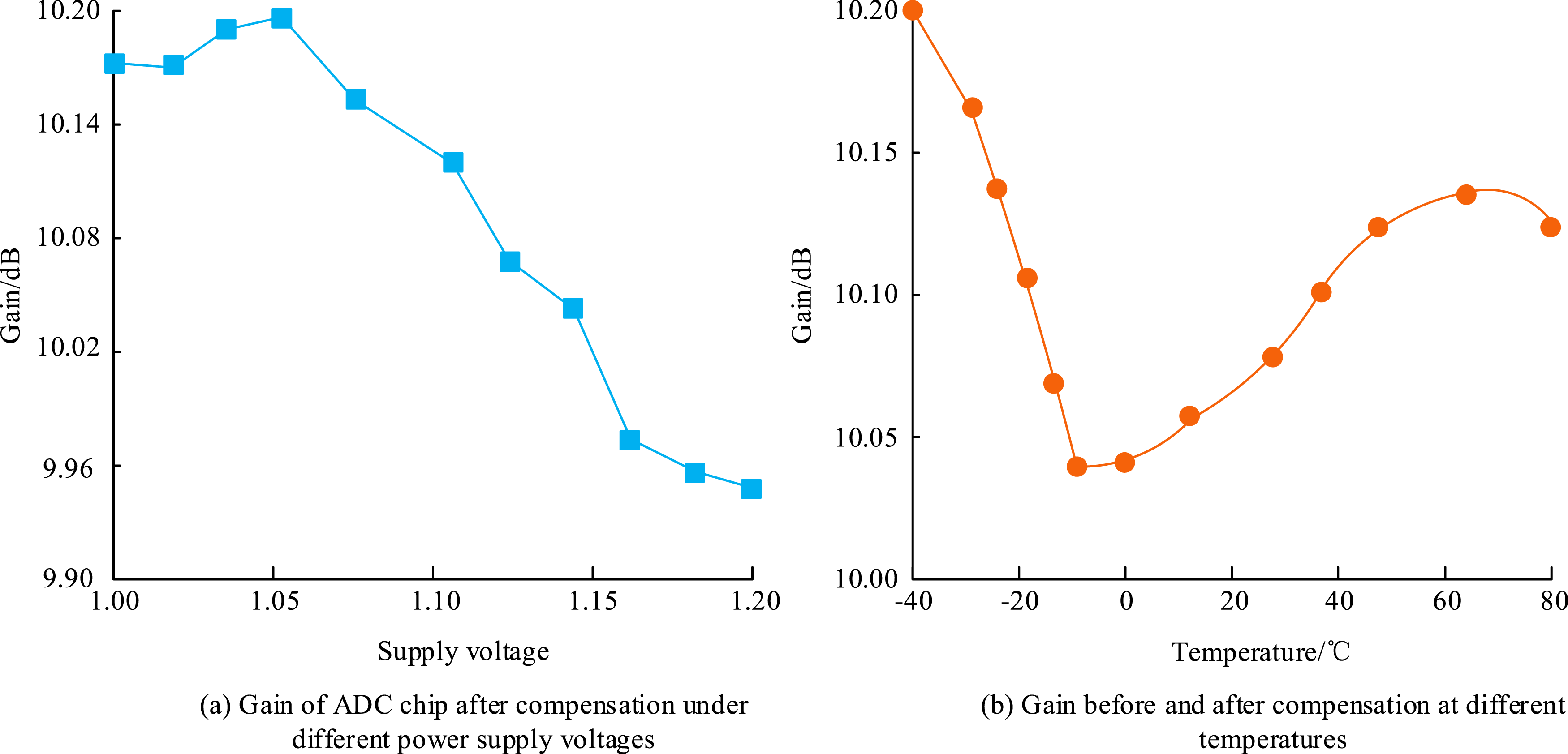
To further verify the voltage resistance of the ADC chip, a simulation test was conducted to compare the error values of the ADC chip before and after compensation, as shown in Figure 9. From Figure 9(a), in terms of voltage tolerance, the compensation measures greatly stabilized the error value, resulting in a significant decrease in error value from 7.01% before compensation to 1.97% at the application point of 1.06 V, an improvement of 5.04%. From Figure 9(b), under extreme temperature conditions as low as −40°C, the maximum error value after compensation was 2.02%, while without compensation, the error value was as high as 21.98%, a decrease of nearly 20%. Overall, the compensated ADC chip exhibited excellent performance in terms of voltage resistance and temperature adaptability. Comparison of error values before and after ADC chip compensation. (a) Error values before and after compensation under different power supply voltages and (b) error values before and after compensation for different temperatures.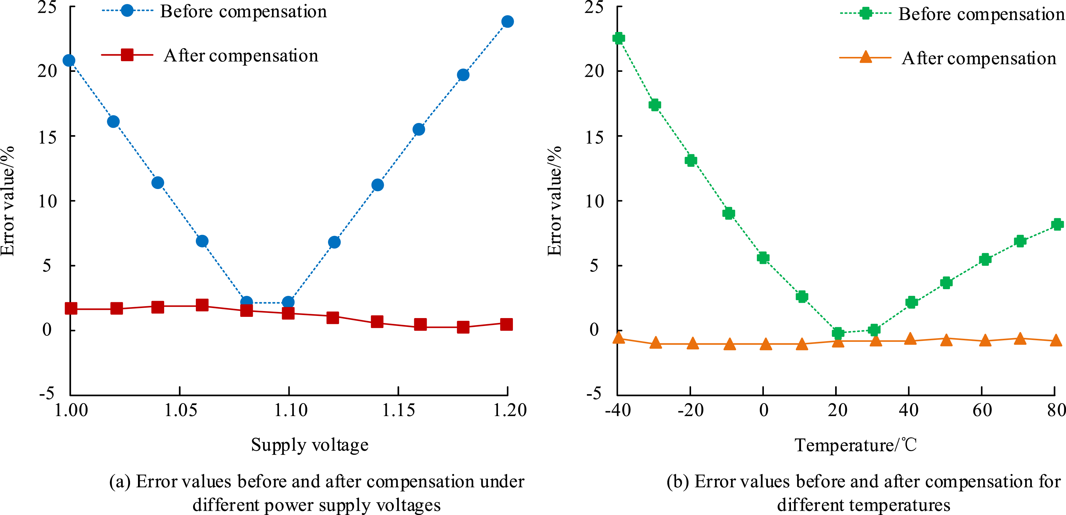
For application devices such as medical monitoring equipment, industrial sensors, and high-speed communication systems that require high precision as their core, reducing errors will directly affect the accuracy of signal sampling. For example, in the field of automotive electronics, high-precision ADC chips are required for data acquisition of various sensors inside cars to ensure the accuracy of safety systems for drivers and passengers. ADC chips with low error and high stability can provide real-time and accurate environmental monitoring data, thereby improving automotive safety.
Errors can usually be divided into two types: systematic errors and random errors. Random errors are caused by uncertain factors and manifest as unpredictable fluctuations, while systematic errors usually have strong regularity. Therefore, sensitivity analysis has become an important tool for further understanding the variation of errors under different conditions. According to the simulation results under different temperature and voltage fluctuation conditions, the variation of system error shows a relatively obvious pattern. For example, in the extreme environment shown in Figure 9(b), after compensation, it decreased to 2.02%, proving that compensation measures can significantly reduce system errors caused by temperature. However, as voltage or temperature conditions further limit, random errors will also increase, especially in extreme environments where the response time and timing control of the chip may lead to an increase in small errors. Therefore, future research needs to conduct error sensitivity analysis within a wider range of temperature and voltage fluctuations to evaluate the interaction between system errors and random errors under different operating conditions, further improving the stability and reliability of chips in various extreme environments.
To verify the effectiveness of the strategy of compensating for the nonlinear behavior of NMOS switches using the inherent diode junction capacitance characteristics of PMOS transistors, a simulation comparative analysis was conducted on the ADC chips before and after improvement, as shown in Figure 10. From Figure 10, when the time reached 2.61 ns, the voltage response of the improved chip increased to 0.8 V, while under the same conditions, the pre improved chip did not reach the same voltage until 2.65 ns. This result indicated that the application of PMOS transistors effectively accelerated the response time of ADC chips, thus it can be seen that this compensation method helps to improve the overall conversion rate. Simulation diagram of ADC chip before and after PMOS transistor improvement.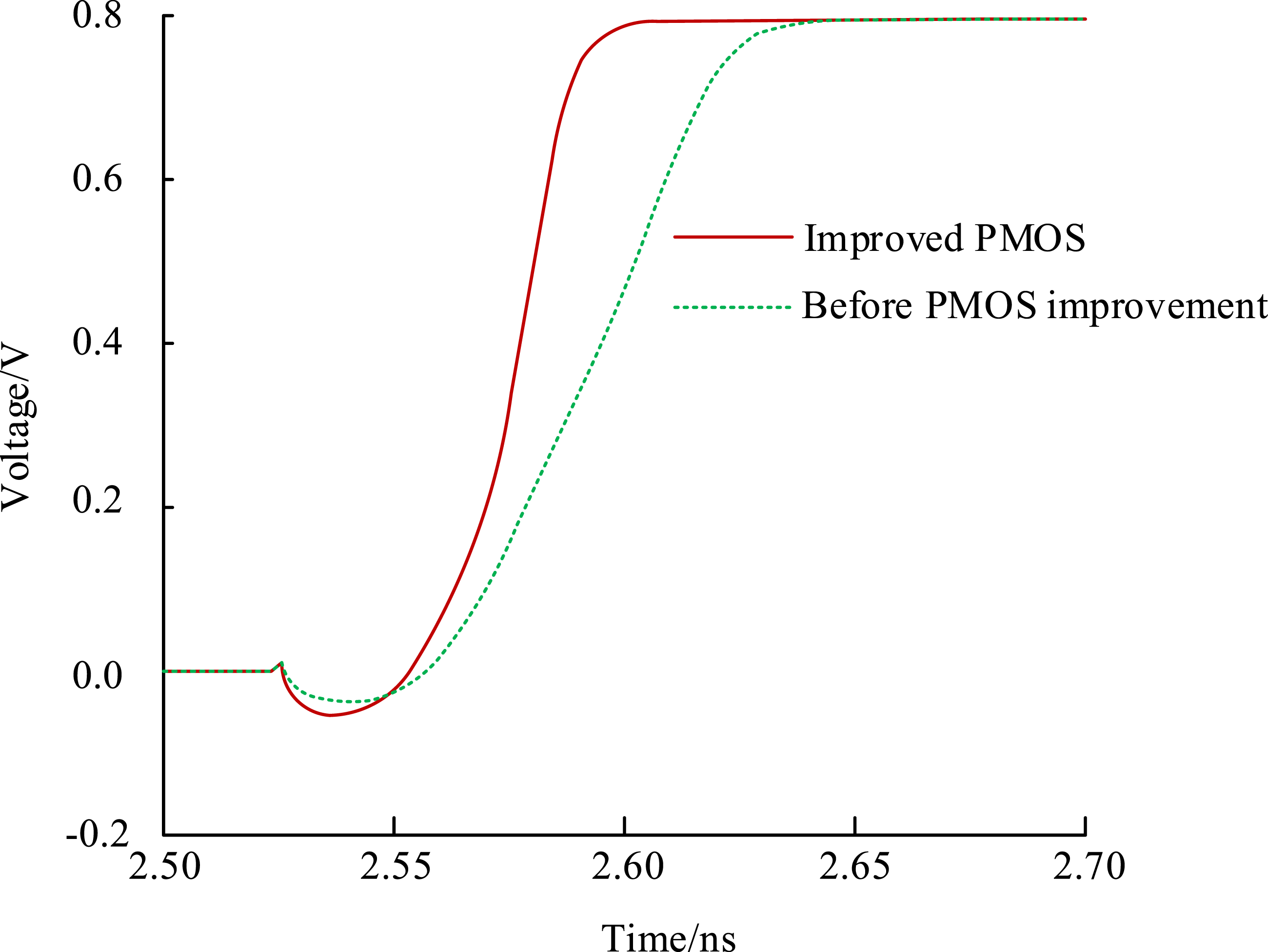
Comparison of performance parameters for different ADC chip designs.
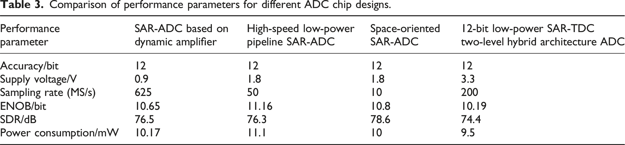
Low-power design has a significant impact on portable electronic devices. Low power consumption means an extension of battery life, which can support devices to operate stably for a long time without frequent charging. This is very important for improving user experience and device convenience. For example, in smart homes, the low-power characteristics of this chip are very suitable for low-power devices such as temperature and humidity sensors, smoke alarms, etc., enabling these devices to operate stably for a long time and reducing dependence on batteries.
Performance comparison of different low power ADC chip designs.

Conclusion
In modern electronic systems, ADC, as a key component, is crucial for applications with high speed and low power consumption performance. To achieve a balance between fast and accurate data conversion and system power consumption, a high-performance 12-bit low-power ADC chip design was studied. The results showed that the SNR and SDR of the chip were 65.1 dB and 74.4 dB, respectively, indicating that the noise content in the signal was extremely low, the signal purity was high, and the distortion was small. Meanwhile, the SNDR and THD of the chip reached 64.9 dB and 78.3 dB, respectively, with an ENOB of 10.19 bits, further demonstrating its high quantization accuracy. In addition, the chip exhibited high gain stability when adjusting the power supply voltage from 1.06 V to 1.20 V. Its maximum gain was 10.18 dB and the minimum gain was 9.95 dB. Even within the extreme temperature range of −40°C to −10°C, the change in gain was only 0.16 dB, demonstrating good temperature stability. The voltage compensation measures significantly improved the performance of the chip at 1.06 V voltage. Through compensation, the error value was significantly reduced from 7.01% to 1.97%, optimizing 5.04%. Under extreme low temperature conditions of −40°C, the maximum error value after compensation was 2.02%, which was significantly improved compared to the uncompensated 21.98%. In summary, the simulation study of voltage resistance testing for 12-bit low-power ADC chips effectively reduced power consumption and enhanced voltage resistance.
However, there is still room for further improvement in research. Future work can be carried out in the following directions: firstly, further optimizing the data exchange mechanism between SAR and TDC modules to improve overall conversion accuracy; the second is to verify its robustness within a wider range of temperature and voltage fluctuations to meet the requirements of more complex application environments; the third is to explore circuit design based on new materials or heterogeneous integrated structures, in order to further break through the limitations of traditional CMOS processes in terms of power consumption and speed. This ADC chip has broad application prospects in fields such as medical imaging, wearable devices, and spacecraft navigation that require both high resolution and low power consumption. Future research can also focus on customized design for different application scenarios, in order to achieve the optimal match between performance and cost.
Although the current sampling rate is significantly better than traditional designs, there may still be a sampling rate bottleneck of 200 MS/s for some ultra-high speed signal processing scenarios. Therefore, future research can enhance the sampling capability of the entire system by improving the time resolution and parallel structure of the TDC module. Meanwhile, multi-phase parallel sampling or time interleaving (TI-ADC) technology can also be introduced to break through the single channel sampling rate limitation while maintaining low power consumption. In addition, future research can explore the possibility of combining SAR-TDC architecture with emerging technologies such as machine learning and artificial intelligence, such as introducing intelligent controllers to achieve adaptive quantization decision-making, or using neural networks for online correction of TDC delay errors.
However, the study did not discuss the performance of chips in more extreme working environments, so the research results are not yet comprehensive. For example, a decrease in the threshold voltage of MOS transistors at high temperatures may cause comparator mismatch or a decrease in sampling accuracy. Exceeding the upper limit of the rated voltage of the device may cause reliability degradation or device breakdown, as well as increased clock delay and analog signal response time under extremely low temperature conditions, which may affect sampling accuracy and timing control. Therefore, future research should consider using methods such as temperature accelerated aging testing and voltage transient impact simulation to further broaden the scope of verification and enhance the robustness and versatility of the design in extreme application environments.
Footnotes

Funding
The authors received no financial support for the research, authorship, and/or publication of this article.
Declaration of conflicting interests
The authors declared no potential conflicts of interest with respect to the research, authorship, and/or publication of this article.