
Abstract
This paper deals with the design and test of a contactless capacitive power converter operating at a frequency of 1 MHz, intended to supply the excitation winding of an 80 kW wound rotor synchronous machine. The methodology integrates the electromagnetic design of the rotor and its impact on the different parameters of the converter. To verify the validity of the concept, a first prototype was built by using surface-mounted capacitors grounded on the structure of a 1 MHz Class E resonant power converter. Then, a more representative capacitive contactless coupler was designed and implemented. Comparisons between simulation and experimental results have shown the limits of the proposed contactless power transmission. Special attention was paid on losses and efficiency which are crucial for this application.
Keywords
Introduction
In the automotive industry, rare-earth permanent magnet synchronous machines (PMSMs) are widely used for traction applications due to their superior power density [1]. However, the use of rare-earth materials, such as neodymium, poses challenges. These materials are not only expensive but also subject to a geographically constrained supply chain. Additionally, there are growing concerns about their ecological impact [2]. An alternative to PMSMs is the wound rotor synchronous machine (WRSM), which can achieve similar power densities, albeit with increased heat generation. A further challenge with WRSMs is the use of brushes on the rotor surface, which complicates the application of oil cooling and raises issues of increased wear and tear. Consequently, the development of brushless, contactless power transfer systems is gaining renewed interest. Historically, inductive power transfer, based on the principle of a rotary transformer [3], was the primary focus and has reached industrial maturity, with its adoption by automotive manufacturers [4]. Until a few years ago, capacitive power transfer (CPT), which does not require magnetic cores, was relatively overlooked due to perceived limitations in achieving comparable power densities with cost-effective technology. This perspective has shifted recently [5], thanks to breakthroughs in high-power electronics at radio frequencies and in the mechanical design of capacitive couplers. First, advances in power electronics, particularly in Silicon Carbide (SiC) and Gallium Nitride (GaN) technologies, have enabled high-efficiency operations in the MHz frequency range at an affordable cost [6]. This development has significantly reduced the capacitance needed for power transfers. Second, there have been substantial improvements in maintaining extremely small air gaps between rotating armatures, greatly enhancing the achievable capacitance within a given volume [7]. These advancements have led to the following achievements: the transmission of 300 W to the rotor of a 10 kW Wound Field Synchronous Generator [8], and the transmission of 1 kW to the rotor winding of an 80 kW WRSM [9]. Despite these significant milestones, the difficulty of achieving high capacity within a small volume remains a technical constraint that hinders the democratization of these applications in the industry.
This paper aims to study the possibility to decrease the required capacitance needed for capacitive power transfer by simultaneously sizing the rotor and the converter. It outlines the design and implementation of a 1MHz class-E resonant converter paired with a simplified axial capacitive coupler, integrating the dimensioning of the rotor winding and its impact on the different parameters. Aiming to refine and reproduce the aforementioned innovations, the study prioritizes identifying patterns that guide the creation of a cost-effective and practical converter. This approach minimizes component use and simplifies the design process to meet the automotive industry’s economic demands, marking a preliminary step towards mastering and applying these advancements effectively.
Coupled rotor sizing, power converter and capacitive coupler design
The overarching goal of the sizing process is to design the rotor, power converter, and capacitive coupler in a way that results in a capacitive coupler with the smallest possible capacitance value. This approach allows for the use of a larger air gap and reduces the required surface area of the electrodes.
Electromagnetic sizing
The sizing of the excitation system is related to the winding that needs to be energized, specifically characterized by its resistance, inductance, and the current that must flow through it. To obtain these values, it’s necessary to perform the sizing of the machine connected to this excitation system. This was achieved through the use of a semi-analytical magnetic model developed in a previous study [10]. This linear model is a 2D one in which the PDEs arising from Maxwell equations are solved by separation of variables using a magnetic vector potential formulation. The ferromagnetic materials have infinite permeability and the stator slots are replaced by an equivalent current sheet. As shown in Fig. 1, only 1 pole of the machine is considered with anti-periodic boundary conditions in the orthoradial direction.
This optimization allows us to define the optimal geometry of the rotor magnetic circuit for the rated operation for which the current density value doesn’t saturate the iron parts. The operation of the machine at its peak power leads to higher currents which heavily saturates the iron part so Finite Element simulations have been carried out to determine the necessary current density.
The geometry of the rotor, along with the computed current density, enables us to determine the total current flowing in the excitation winding. The total ampere-turns being equal to the product of the slot’s cross section area S by the current density J we can then compute the current by Eq. (1):
The resistance of the rotor winding is then given by:
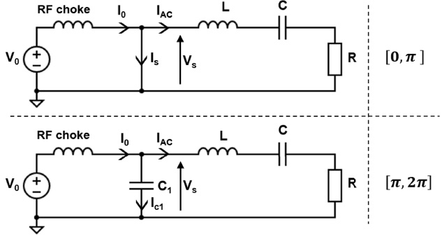
As illustrated in Fig.2, the key idea of the excitation system is to use a high-frequency resonant converter whose resonant capacitor is used to achieve contactless capacitive power transfer. The choice of the converter topology (Class E) was based on the studies of Dai [11] that compared the different topologies used for capacitive contactless power transfer. The advantages of this converter proposed by Sokal and Sokal [12], are its simplicity, requiring only one transistor, and its high efficiency due to the transistor operating under zero voltage switching conditions (ZVS) and zero voltage derivative condition (ZVDS).

2D geometry of 1 pole of the machine used for the analytical model.

Circuit diagram of Class E contactless power converter with a full-bridge rectifier.
The design of the converter is based on the methodology provided by Kazimierczuk [13]. The operating frequency, f, is set at 1 MHz to minimize the size of the capacitor required for the contactless system. This choice is facilitated by the availability of Silicon Carbide (SiC) MOSFETs capable of operating at such a high frequency. The analysis assumes that the input current, I0 is perfectly smoothed and that the ac current in the resonant circuit, I AC , is perfectly sinusoidal, which is achievable if the quality factor of the circuit, Q L , exceeds 2.5. The diode rectifier is assumed to be an ideal full-bridge rectifier. Owing the high switching frequency, the current I in the rotor is smoothed by the inductance Lrotor, so it is considered ripples free. These assumptions simplify the circuit analysis for each transistor state as depicted in Fig. 3 and enable the derivation of transient equations governing the system’s behavior in each transistor state related to the duty cycle d. The conducting phase of transistor corresponds to 𝜔t ∈ [0, 𝜋], then V s = 0 in this interval.
Different states of the converter for
By setting:
The assumption of the full-bridge rectifier being ideal leads to:
Simplified equivalent resonant circuit.
Since I
AC
is sinusoidal, we can consider that only the fundamental voltage components are present, and therefore, by applying Kirchhoff’s Voltage Law, we can write:
The first step involves the magnetic optimization of the rotor using the electromagnetic models, which yields to the mean current density in the slot at peak operating point as well as the slot dimensions. The results of the rotor optimization for our case study are presented in Table 1. Details on the optimization process are beyond the scope of this paper.
Results of the rotor optimization
Results of the rotor optimization
The equations presented in Section 2.2 allow us to express all parameters and voltages as a function of the number of conductors N. Setting a value for the quality factor Q L ultimately enables us to obtain a set of parameters for each value of N.
Adding dielectric and spatial constraints related to the dimensions of the capacitive coupler allows us to complete this study. First, the value of the coupler’s capacitance, calculated using the classic formula for a planar capacitor, must be low enough so that its volume does not exceed the available space for its implementation. Finally, the capacitor C being divided into two capacitors in series (forward and return, as illustrated in Fig. 2), the voltage across one capacitor in series, equal to 2V
c
, must be lower than the breakdown voltage:
Constraints and parameters used for the study
The variations in the parameters C, L, and R as a function of N for different values of Q L are illustrated in Fig. 5.

Evolution of R, L, and C as functions of N for different values of Q L and evolution of the product LC𝜔2 as a function of Q L. Red circles indicate operating points where constraints on maximum switch voltage or maximum capacitor voltage were not met.
Figure 5 illustrates that an increase in the quality factor is associated with a decrease in the product of 𝜔2, inductance L and capacitance C, which reflects a reduction in the overall dimensions of components L and C at a given operating frequency. Specifically, a high value of the quality factor contributes to decrease of the capacitance C, which is crucial for reducing the size of capacitive couplers—a significant obstacle to their broader acceptance. However, the primary challenge arises from the inductance value L, which increases with the quality factor Q L . This increase of L can be limited by technical constraints or by the physical space available for component integration.
The values selected for the experimental work corresponds to N = 63. This decision was influenced by the ease of implementation using our equipment. These values are detailed in Table 3 and are highlighted in Fig. 5.
Set of parameters chosen for the experimental setup
Design of the contactless capacitive coupler
The contactless coupler, designed to validate the concept, was created with a simple geometry that approximates the volume found in a vehicle traction motor housing. The axial field capacitive coupler, depicted in Fig. 6, consists of aluminum discs designed for shaft mounting, with every second disc internally connected to form one electrode (intended to be mounted on the shaft). The same applies to the alternate discs, which are connected on the outer part (intended to be affixed to the housing). Each coupler must have a capacitance of 3.72 nF (2C). Eddy currents and conductive losses were neglected, the plates thickness being much larger than two times the skin depth at 1 MHz [14]. Parasitic capacitances were also neglected, as no housing is used yet and the distance between the two couplers being higher than the airgap length by orders of magnitude. The constraints on volume and the choice of air gap length (0.3 mm) determine the surface area and the number of discs, the capacitance of each coupler is computed using a classical formula. The design was verified by 3D finite element simulations using COMSOL Multiphysics electrostatic module, as shown in Fig. 7. The capacity calculated by simulation of the two couplers in series was 1.90 nF.
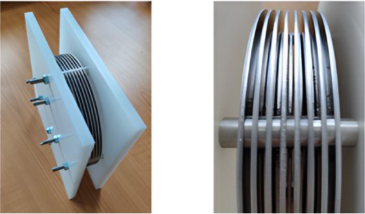
Prototype for the capacitive coupler. Left: whole coupler. Right: zoomed view of plates and airgap.
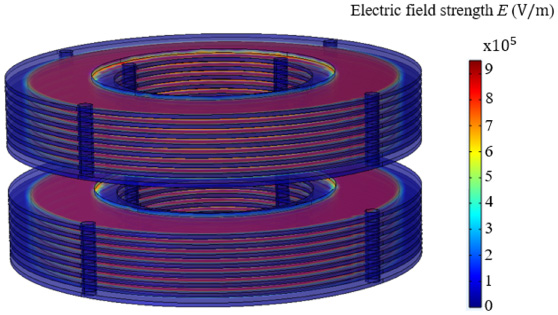
3D finite element simulation (COMSOL Multiphysics electrostatic module) of the two couplers in series showing the distribution of the electric field strength.
Mechanical considerations were deferred in this study, with static couplers featuring bars and spacers to maintain connections and air gaps. The capacitance values of the two manufactured couplers were measured at 3.93 nF and 3.79 nF at 1 Mhz, respectively, using an LCR meter. Figure 8 shows the impedance caracteristic of one of the couplers and confirms the hypothesises adopted during its sizing, the coupler exhibits almost purely capacitive characteristics at 1 MHz.

Characterization of one coupler with a LCR meter.
A prototype integrating the power converter and the contactless coupler has been developed, facilitating swift transitions between two configurations: one featuring surface-mounted capacitors in the resonnant circuit and the other equipped with the sized contactless coupler, replacing the ceramic capacitors, as depicted in Fig. 9. These two distinct setups allow for the evaluation of the Class E converter initially, followed by the assessment of the impact of substituting the coupler for ceramic capacitors. The setup, connected with Litz wire, includes a Mosfet driver and power block (KIT8020CRD8FF1217P-1 SiC Mosfet evaluation kit driving a C2M0025120D SiC Mosfet), a custom PCB with surface-mounted capacitors forming the resonant circuit alongside a 15 μH air-core inductor (constructed with Litz wire), and a full-wave rectifier bridge comprising four SiC diodes (C4D40120D).

Whole setup of the power converter plus contactless condensator prototypes.
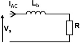
This is followed by an inductor and a resistor emulating the wound rotor’s impedance, as illustrated in Fig. 2. Both configurations, utilizing surface-mounted capacitors and the coupler prototype, shown in Fig. 9, were tested at an operating point with an output DC current of 4 A. Efficiency measurements across the different parts of the system were then compared to identify circuit losses, as indicated in Fig. 11. Finally, both setups were progressively taken to their limits by increasing the input voltage until total failure occurred, which was due to the dielectric breakdown of either the surface-mounted capacitors or the contactless couplers.
The waveforms of the main currents in the converter equipped with the capacitive coupler (operating at 4A output) are depicted in Fig. 10. They confirm that the converter is working as intended, both in the inverter and rectifier sections, showing indeed the presence of AC current in the resonant loop, and rectified current in the load.

Currents in the resonant loop, I AC , and in the load I (setup equipped with the capacitive coupler, operating at 4 A output).

Efficiencies derived from power measurement at differents points of the converter.
The first setup, which utilizes a surface-mounted capacitor, achieved an output of 720 W/10 A with an overall efficiency of 62%. This outcome is promising and can be primarily attributed to the principal losses occurring at the switch, as shown in Fig. 11. Frequency analysis conducted at the same power level indicated that the optimal overall efficiency (75%) was achieved at 920 kHz, as presented in Fig. 12. While this points to issues with tuning and uncertainty in parameter identification, the fact that the previous version of this setup attained an efficiency of 80%—although not suited for high-power applications—indicates that these problems can be addressed in future research.

Frequency sweep.
The second setup, equipped with the capacitive contactless converter, achieved an output of 192 W with an overall efficiency of 38%. As shown in Fig. 11, the resonant circuit is responsible for the significant losses. In this configuration, a frequency sweep also confirmed that the highest overall efficiency (45%) occurred at a frequency of 940 kHz, as depicted in Fig. 12. This again suggests issues with tuning and uncertainty in parameter identification. Despite the absence of excess heat or visible defects, design issues—particularly those concerning the maintenance of the challenging 0.3 mm air gap—might be to blame and could explain the substantial efficiency discrepancy with the first setup. Another area for investigation could be the electrical continuity and potential contact resistances between the aluminum plates.
A comparison of the MOSFET voltages was made, as illustrated in Fig. 13, and showed that the zero-voltage-switching conditions for the MOSFETs were not ideal, confirming the hypothesis that tuning issues were causing the converter to operate in non-optimal conditions, hence the increased losses located at the MOSFET and in the resonant loop. Final conclusions on these issues are still pending due to the destruction of our prototypes during the most recent tests.

Comparison of Mosfet drain-source voltage waveforms at the same operating point corresponding to a DC output current of 4 A.
This paper presents a comprehensive study on the design, parameters, and integration of a complete system that includes a 1 MHz Class E converter with SiC components, a capacitive coupler for contactless power transmission, and the selection of rotor winding. The integrated approach not only addresses the system’s design comprehensively but also focuses on optimizing these components to enhance cost-efficiency and ease of implementation. The analysis highlights a trend towards increased system compactness, which is vital for cost reduction—a critical factor in the automotive industry. This compactness significantly facilitates the implementation of the capacitive coupler, emphasizing the design’s practical benefits in reducing size, economic impact, and simplifying deployment. An implementation of the Class E converter using ceramic capacitors was achieved, delivering an output of 720 W/10 A with an overall efficiency of 62%. Furthermore, a capacitive coupler was developed and tested within the resonant circuit, serving to explore the capabilities of contactless capacitive power transfer. This setup attained an output of 192 W/5 A with an efficiency of 38%. The subsequent analysis indicates that the primary, unexpected, losses could be due to tuning issues, associated with unanticipated behaviors of the capacitive coupler and potential design methodology limitations, alongside the challenge of maintaining a precise 0.3 mm air gap. Future efforts will concentrate on addressing these tuning issues to substantially mitigate these unexpected losses. The insights gained from this study are crucial for boosting the converter’s power output, developing a regulation system, and improving the capacitive couplers’ mechanical design. Informed by the initial design and sizing efforts, this strategy underscores the method’s potential to better optimize the entire system (rotor and excitation system), especially within industries sensitive to costs, such as the automotive sector.
Footnotes
Acknowledgements
We would like to thank Nidec-PSA-Emotors for their financial support of our research. Their contribution was crucial in enabling the progress and completion of our work.